EP0293235A2 - Anzeigegerät und Ansteuersystem dafür - Google Patents
Anzeigegerät und Ansteuersystem dafür Download PDFInfo
- Publication number
- EP0293235A2 EP0293235A2 EP88304846A EP88304846A EP0293235A2 EP 0293235 A2 EP0293235 A2 EP 0293235A2 EP 88304846 A EP88304846 A EP 88304846A EP 88304846 A EP88304846 A EP 88304846A EP 0293235 A2 EP0293235 A2 EP 0293235A2
- Authority
- EP
- European Patent Office
- Prior art keywords
- scanning
- electrodes
- display device
- frame
- signals
- Prior art date
- Legal status (The legal status is an assumption and is not a legal conclusion. Google has not performed a legal analysis and makes no representation as to the accuracy of the status listed.)
- Granted
Links
Images



Classifications
-
- G—PHYSICS
- G09—EDUCATION; CRYPTOGRAPHY; DISPLAY; ADVERTISING; SEALS
- G09G—ARRANGEMENTS OR CIRCUITS FOR CONTROL OF INDICATING DEVICES USING STATIC MEANS TO PRESENT VARIABLE INFORMATION
- G09G3/00—Control arrangements or circuits, of interest only in connection with visual indicators other than cathode-ray tubes
- G09G3/20—Control arrangements or circuits, of interest only in connection with visual indicators other than cathode-ray tubes for presentation of an assembly of a number of characters, e.g. a page, by composing the assembly by combination of individual elements arranged in a matrix no fixed position being assigned to or needed to be assigned to the individual characters or partial characters
- G09G3/34—Control arrangements or circuits, of interest only in connection with visual indicators other than cathode-ray tubes for presentation of an assembly of a number of characters, e.g. a page, by composing the assembly by combination of individual elements arranged in a matrix no fixed position being assigned to or needed to be assigned to the individual characters or partial characters by control of light from an independent source
- G09G3/36—Control arrangements or circuits, of interest only in connection with visual indicators other than cathode-ray tubes for presentation of an assembly of a number of characters, e.g. a page, by composing the assembly by combination of individual elements arranged in a matrix no fixed position being assigned to or needed to be assigned to the individual characters or partial characters by control of light from an independent source using liquid crystals
- G09G3/3611—Control of matrices with row and column drivers
- G09G3/3622—Control of matrices with row and column drivers using a passive matrix
- G09G3/3644—Control of matrices with row and column drivers using a passive matrix with the matrix divided into sections
-
- G—PHYSICS
- G09—EDUCATION; CRYPTOGRAPHY; DISPLAY; ADVERTISING; SEALS
- G09G—ARRANGEMENTS OR CIRCUITS FOR CONTROL OF INDICATING DEVICES USING STATIC MEANS TO PRESENT VARIABLE INFORMATION
- G09G2310/00—Command of the display device
- G09G2310/02—Addressing, scanning or driving the display screen or processing steps related thereto
- G09G2310/0224—Details of interlacing
- G09G2310/0227—Details of interlacing related to multiple interlacing, i.e. involving more fields than just one odd field and one even field
-
- G—PHYSICS
- G09—EDUCATION; CRYPTOGRAPHY; DISPLAY; ADVERTISING; SEALS
- G09G—ARRANGEMENTS OR CIRCUITS FOR CONTROL OF INDICATING DEVICES USING STATIC MEANS TO PRESENT VARIABLE INFORMATION
- G09G2320/00—Control of display operating conditions
- G09G2320/02—Improving the quality of display appearance
- G09G2320/0247—Flicker reduction other than flicker reduction circuits used for single beam cathode-ray tubes
Definitions
- the present invention is effective for the condition of 60 > in which "r" is the time required for rewriting the picture elements in one horizontal scanning period.
- a display device such as an X-Y matrix type liquid crystal display panel contains a pair of insulating substrates with a liquid crystal layer sandwiched therebetween.
- "M" pcs. of scanning electrodes are provided on the inner side of one of the substrates, and "N” pcs. of signal electrodes on the inner side of the other substrate, the scanning electrodes crossing the signal electrodes at a right angle.
- the display device of the present invention provides an incomplete memory characteristic and takes "r" seconds to rewrite the picture elements in one horizontal scanning period.
- An example of a substrate with an incomplete memory characteristic is ferrodielectric liquid crystal.
- Image data to be supplied to the signal electrodes Y1, Y2, ... Y640 is sent in form of input signals Ei through a terminal 3 to a shift register 6 which comprises D flip flops R1, R2, ... R640 corresponding to the signal electrodes respectively.
- the input signals Ei are applied to the data terminals of the D flip flops R1, R2, ... R640.
- a basic clock pulse signal C is supplied from a converter circuit 2 to the clock terminals of the D flip flops R1, R2, ... R640 so that data signals are output sequentially from the D flip flops R1, R2, ... R640 in this order.
- the data signals thus output pass through D flip flops r1, r2, ...
- the D flip flop b1 On receiving a selection signal and a horizontal clock pulse signal, the D flip flop b1 supplies an output equivalent to the selection signal to the following D flip flop b K+1 simultaneously as it supplies rewrite signal to the scanning electrode L1.
- the D flip flop b K+1 on receiving the signal output from the D flip flop b1 and a horizontal clock pulse signal C1, outputs rewrite signal to the scanning electrode L K+1 and simultaneously supplies an output equivalent to the selection signal to the following D flip flop.
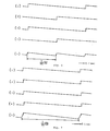
- the scanning electrodes of the same order in all groups are rewritten sequentially in the same frame period.
- the first scanning electrodes of the groups are scanned first, and the second scanning electrodes of the groups are scanned next. This process is repeated until the K′th electrode ot the groups are scanned.
- 2P′ scanning electrodes are scanned in each time, and the scanning operation is conducted K′ times to rewrite the picture on an entire display panel divided into the first and the second display blocks.
- the selection signals U1 are supplied to D flip flops b1 and b101, and the selection signals U2 to D flip flops b2 and b102.
- the output from the D flip flop b1 is given to the first scanning electrode L1 via a scanning electrode driver a1.
- the output from the D flip flop b101 is given to the scanning electrode L101 in the second display block 1B via a scanning electrode driver a101.
- D flip flops b3, b5, ... b99 are connected in series after the D flip flop b1, but they are not shown in Fig. 3.
- selection signals U1 are supplied to the data terminals of the D flip flops b1 and b101.
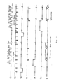
- the D flip flops b1 and b101 supply the scanning electrodes L1 and L101 with the output P1 shown in Fig. 5.
- the outputs P1 are also input to the data terminals of the following D flip flops b3 and b103 (not shown).
- the D flip flops b3 and b103 output signals P3 of Fig. 5 to the scanning electrodes L3 and L103.
Landscapes
- Engineering & Computer Science (AREA)
- Chemical & Material Sciences (AREA)
- Crystallography & Structural Chemistry (AREA)
- Physics & Mathematics (AREA)
- Computer Hardware Design (AREA)
- General Physics & Mathematics (AREA)
- Theoretical Computer Science (AREA)
- Liquid Crystal Display Device Control (AREA)
- Transforming Electric Information Into Light Information (AREA)
Applications Claiming Priority (2)
| Application Number | Priority Date | Filing Date | Title |
|---|---|---|---|
| JP133816/87 | 1987-05-29 | ||
| JP62133816A JP2635967B2 (ja) | 1987-05-29 | 1987-05-29 | 強誘電性液晶デバイスの駆動方法 |
Publications (3)
| Publication Number | Publication Date |
|---|---|
| EP0293235A2 true EP0293235A2 (de) | 1988-11-30 |
| EP0293235A3 EP0293235A3 (en) | 1990-03-07 |
| EP0293235B1 EP0293235B1 (de) | 1995-05-03 |
Family
ID=15113712
Family Applications (1)
| Application Number | Title | Priority Date | Filing Date |
|---|---|---|---|
| EP19880304846 Expired - Lifetime EP0293235B1 (de) | 1987-05-29 | 1988-05-27 | Anzeigegerät und Ansteuersystem dafür |
Country Status (3)
| Country | Link |
|---|---|
| EP (1) | EP0293235B1 (de) |
| JP (1) | JP2635967B2 (de) |
| DE (1) | DE3853697T2 (de) |
Cited By (2)
| Publication number | Priority date | Publication date | Assignee | Title |
|---|---|---|---|---|
| US5206632A (en) * | 1989-09-11 | 1993-04-27 | Deutsche Thomson-Brandt Gmbh | Actuating circuit for a liquid crystal display |
| US5289173A (en) * | 1990-09-27 | 1994-02-22 | Sharp Kabushiki Kaisha | Display control method having partial rewriting operation |
Family Cites Families (2)
| Publication number | Priority date | Publication date | Assignee | Title |
|---|---|---|---|---|
| JPS57201294A (en) * | 1981-06-04 | 1982-12-09 | Suwa Seikosha Kk | Matrix type video display unit |
| JPS6180226A (ja) * | 1984-09-28 | 1986-04-23 | Toshiba Corp | アクテイブ・マトリツクス駆動装置 |
-
1987
- 1987-05-29 JP JP62133816A patent/JP2635967B2/ja not_active Expired - Lifetime
-
1988
- 1988-05-27 DE DE19883853697 patent/DE3853697T2/de not_active Expired - Lifetime
- 1988-05-27 EP EP19880304846 patent/EP0293235B1/de not_active Expired - Lifetime
Cited By (2)
| Publication number | Priority date | Publication date | Assignee | Title |
|---|---|---|---|---|
| US5206632A (en) * | 1989-09-11 | 1993-04-27 | Deutsche Thomson-Brandt Gmbh | Actuating circuit for a liquid crystal display |
| US5289173A (en) * | 1990-09-27 | 1994-02-22 | Sharp Kabushiki Kaisha | Display control method having partial rewriting operation |
Also Published As
| Publication number | Publication date |
|---|---|
| JPS63298286A (ja) | 1988-12-06 |
| JP2635967B2 (ja) | 1997-07-30 |
| EP0293235B1 (de) | 1995-05-03 |
| DE3853697D1 (de) | 1995-06-08 |
| DE3853697T2 (de) | 1996-01-11 |
| EP0293235A3 (en) | 1990-03-07 |
Similar Documents
| Publication | Publication Date | Title |
|---|---|---|
| US4926168A (en) | Liquid crystal display device having a randomly determined polarity reversal frequency | |
| KR100902764B1 (ko) | 콜레스테릭 액정 디스플레이 및 드라이버 | |
| JP3666318B2 (ja) | 電気光学装置及びそれを用いた電子機器並びに表示駆動ic | |
| JP2002196731A (ja) | マルチフレーム反転機能を有する液晶表示装置とその駆動装置及び方法 | |
| US5298913A (en) | Ferroelectric liquid crystal display device and driving system thereof for driving the display by an integrated scanning method | |
| EP0261899A2 (de) | Aufzeichnungsvorrichtung | |
| US6392631B1 (en) | Process for displaying data on a matrix display | |
| JP3110618B2 (ja) | 液晶表示装置 | |
| US5969713A (en) | Drive circuit for a matrix-type display apparatus | |
| US4701025A (en) | Liquid crystal display device with driving method to eliminate blur due to frequency dependence | |
| JP3056631B2 (ja) | 液晶表示装置 | |
| EP0293235B1 (de) | Anzeigegerät und Ansteuersystem dafür | |
| EP0435701A2 (de) | Verfahren und Einrichtung zum Steuern einer ferroelektrischen Flüssigkristallanzeigetafel | |
| KR970022927A (ko) | 액정 표시 장치 및 그 구동 방법 | |
| CN116027931A (zh) | 触控显示驱动电路、驱动方法及触控显示面板 | |
| JP3233010B2 (ja) | 液晶表示装置 | |
| EP0478382A2 (de) | Verfahren und Einrichtung zum Steuern eines Flüssigkristallanzeigegeräts | |
| EP1614096A1 (de) | Anzeigevorrichtung | |
| JP2575189B2 (ja) | 液晶装置 | |
| CN102483532B (zh) | 双稳态液晶显示面板及其驱动方法 | |
| KR20010023722A (ko) | 다른 비디오 표준들로부터의 비디오 신호들을디스플레이하도록 적합된 매트릭스 디스플레이 장치 | |
| EP0614563B1 (de) | Flüssigkristallanseigevorrichtung | |
| KR950019824A (ko) | 매트릭스형 액정표시장치의 구동장치 및 그 구동방법 | |
| JP3024167B2 (ja) | 液晶表示駆動装置 | |
| JPS6363094A (ja) | 表示装置 |
Legal Events
| Date | Code | Title | Description |
|---|---|---|---|
| PUAI | Public reference made under article 153(3) epc to a published international application that has entered the european phase |
Free format text: ORIGINAL CODE: 0009012 |
|
| AK | Designated contracting states |
Kind code of ref document: A2 Designated state(s): DE GB |
|
| PUAL | Search report despatched |
Free format text: ORIGINAL CODE: 0009013 |
|
| AK | Designated contracting states |
Kind code of ref document: A3 Designated state(s): DE GB |
|
| 17P | Request for examination filed |
Effective date: 19900327 |
|
| 17Q | First examination report despatched |
Effective date: 19920127 |
|
| GRAA | (expected) grant |
Free format text: ORIGINAL CODE: 0009210 |
|
| AK | Designated contracting states |
Kind code of ref document: B1 Designated state(s): DE GB |
|
| REF | Corresponds to: |
Ref document number: 3853697 Country of ref document: DE Date of ref document: 19950608 |
|
| PLBE | No opposition filed within time limit |
Free format text: ORIGINAL CODE: 0009261 |
|
| STAA | Information on the status of an ep patent application or granted ep patent |
Free format text: STATUS: NO OPPOSITION FILED WITHIN TIME LIMIT |
|
| 26N | No opposition filed | ||
| REG | Reference to a national code |
Ref country code: GB Ref legal event code: IF02 |
|
| PGFP | Annual fee paid to national office [announced via postgrant information from national office to epo] |
Ref country code: DE Payment date: 20070524 Year of fee payment: 20 |
|
| PGFP | Annual fee paid to national office [announced via postgrant information from national office to epo] |
Ref country code: GB Payment date: 20070523 Year of fee payment: 20 |
|
| REG | Reference to a national code |
Ref country code: GB Ref legal event code: PE20 Expiry date: 20080526 |
|
| PG25 | Lapsed in a contracting state [announced via postgrant information from national office to epo] |
Ref country code: GB Free format text: LAPSE BECAUSE OF EXPIRATION OF PROTECTION Effective date: 20080526 |