EP0261899A2 - Aufzeichnungsvorrichtung - Google Patents
Aufzeichnungsvorrichtung Download PDFInfo
- Publication number
- EP0261899A2 EP0261899A2 EP87308312A EP87308312A EP0261899A2 EP 0261899 A2 EP0261899 A2 EP 0261899A2 EP 87308312 A EP87308312 A EP 87308312A EP 87308312 A EP87308312 A EP 87308312A EP 0261899 A2 EP0261899 A2 EP 0261899A2
- Authority
- EP
- European Patent Office
- Prior art keywords
- pixel
- counter
- pixels
- display device
- signal
- Prior art date
- Legal status (The legal status is an assumption and is not a legal conclusion. Google has not performed a legal analysis and makes no representation as to the accuracy of the status listed.)
- Withdrawn
Links
- 239000004973 liquid crystal related substance Substances 0.000 claims abstract description 8
- 238000000034 method Methods 0.000 claims description 7
- 230000000694 effects Effects 0.000 claims description 5
- 238000001514 detection method Methods 0.000 claims description 4
- 210000002858 crystal cell Anatomy 0.000 claims description 3
- 238000012544 monitoring process Methods 0.000 claims 1
- 239000011159 matrix material Substances 0.000 abstract description 2
- 230000007246 mechanism Effects 0.000 abstract description 2
- 238000010586 diagram Methods 0.000 description 4
- 230000005540 biological transmission Effects 0.000 description 3
- 239000005262 ferroelectric liquid crystals (FLCs) Substances 0.000 description 3
- 230000008901 benefit Effects 0.000 description 2
- 239000003990 capacitor Substances 0.000 description 2
- 210000004027 cell Anatomy 0.000 description 2
- 239000000463 material Substances 0.000 description 2
- 230000004048 modification Effects 0.000 description 2
- 238000012986 modification Methods 0.000 description 2
- 230000018199 S phase Effects 0.000 description 1
- XUIMIQQOPSSXEZ-UHFFFAOYSA-N Silicon Chemical compound [Si] XUIMIQQOPSSXEZ-UHFFFAOYSA-N 0.000 description 1
- 230000008859 change Effects 0.000 description 1
- 238000000151 deposition Methods 0.000 description 1
- 239000012769 display material Substances 0.000 description 1
- 230000006870 function Effects 0.000 description 1
- 230000004927 fusion Effects 0.000 description 1
- 229910052710 silicon Inorganic materials 0.000 description 1
- 239000010703 silicon Substances 0.000 description 1
- 230000003068 static effect Effects 0.000 description 1
Images

Classifications
-
- G—PHYSICS
- G09—EDUCATION; CRYPTOGRAPHY; DISPLAY; ADVERTISING; SEALS
- G09G—ARRANGEMENTS OR CIRCUITS FOR CONTROL OF INDICATING DEVICES USING STATIC MEANS TO PRESENT VARIABLE INFORMATION
- G09G3/00—Control arrangements or circuits, of interest only in connection with visual indicators other than cathode-ray tubes
- G09G3/20—Control arrangements or circuits, of interest only in connection with visual indicators other than cathode-ray tubes for presentation of an assembly of a number of characters, e.g. a page, by composing the assembly by combination of individual elements arranged in a matrix no fixed position being assigned to or needed to be assigned to the individual characters or partial characters
- G09G3/34—Control arrangements or circuits, of interest only in connection with visual indicators other than cathode-ray tubes for presentation of an assembly of a number of characters, e.g. a page, by composing the assembly by combination of individual elements arranged in a matrix no fixed position being assigned to or needed to be assigned to the individual characters or partial characters by control of light from an independent source
- G09G3/36—Control arrangements or circuits, of interest only in connection with visual indicators other than cathode-ray tubes for presentation of an assembly of a number of characters, e.g. a page, by composing the assembly by combination of individual elements arranged in a matrix no fixed position being assigned to or needed to be assigned to the individual characters or partial characters by control of light from an independent source using liquid crystals
- G09G3/3611—Control of matrices with row and column drivers
- G09G3/3648—Control of matrices with row and column drivers using an active matrix
- G09G3/3651—Control of matrices with row and column drivers using an active matrix using multistable liquid crystals, e.g. ferroelectric liquid crystals
-
- H—ELECTRICITY
- H04—ELECTRIC COMMUNICATION TECHNIQUE
- H04N—PICTORIAL COMMUNICATION, e.g. TELEVISION
- H04N3/00—Scanning details of television systems; Combination thereof with generation of supply voltages
- H04N3/10—Scanning details of television systems; Combination thereof with generation of supply voltages by means not exclusively optical-mechanical
- H04N3/12—Scanning details of television systems; Combination thereof with generation of supply voltages by means not exclusively optical-mechanical by switched stationary formation of lamps, photocells or light relays
- H04N3/127—Scanning details of television systems; Combination thereof with generation of supply voltages by means not exclusively optical-mechanical by switched stationary formation of lamps, photocells or light relays using liquid crystals
-
- G—PHYSICS
- G09—EDUCATION; CRYPTOGRAPHY; DISPLAY; ADVERTISING; SEALS
- G09G—ARRANGEMENTS OR CIRCUITS FOR CONTROL OF INDICATING DEVICES USING STATIC MEANS TO PRESENT VARIABLE INFORMATION
- G09G2300/00—Aspects of the constitution of display devices
- G09G2300/08—Active matrix structure, i.e. with use of active elements, inclusive of non-linear two terminal elements, in the pixels together with light emitting or modulating elements
- G09G2300/0809—Several active elements per pixel in active matrix panels
- G09G2300/0828—Several active elements per pixel in active matrix panels forming a digital to analog [D/A] conversion circuit
-
- G—PHYSICS
- G09—EDUCATION; CRYPTOGRAPHY; DISPLAY; ADVERTISING; SEALS
- G09G—ARRANGEMENTS OR CIRCUITS FOR CONTROL OF INDICATING DEVICES USING STATIC MEANS TO PRESENT VARIABLE INFORMATION
- G09G2330/00—Aspects of power supply; Aspects of display protection and defect management
- G09G2330/12—Test circuits or failure detection circuits included in a display system, as permanent part thereof
-
- G—PHYSICS
- G09—EDUCATION; CRYPTOGRAPHY; DISPLAY; ADVERTISING; SEALS
- G09G—ARRANGEMENTS OR CIRCUITS FOR CONTROL OF INDICATING DEVICES USING STATIC MEANS TO PRESENT VARIABLE INFORMATION
- G09G3/00—Control arrangements or circuits, of interest only in connection with visual indicators other than cathode-ray tubes
- G09G3/20—Control arrangements or circuits, of interest only in connection with visual indicators other than cathode-ray tubes for presentation of an assembly of a number of characters, e.g. a page, by composing the assembly by combination of individual elements arranged in a matrix no fixed position being assigned to or needed to be assigned to the individual characters or partial characters
- G09G3/2007—Display of intermediate tones
- G09G3/2014—Display of intermediate tones by modulation of the duration of a single pulse during which the logic level remains constant
-
- G—PHYSICS
- G09—EDUCATION; CRYPTOGRAPHY; DISPLAY; ADVERTISING; SEALS
- G09G—ARRANGEMENTS OR CIRCUITS FOR CONTROL OF INDICATING DEVICES USING STATIC MEANS TO PRESENT VARIABLE INFORMATION
- G09G3/00—Control arrangements or circuits, of interest only in connection with visual indicators other than cathode-ray tubes
- G09G3/20—Control arrangements or circuits, of interest only in connection with visual indicators other than cathode-ray tubes for presentation of an assembly of a number of characters, e.g. a page, by composing the assembly by combination of individual elements arranged in a matrix no fixed position being assigned to or needed to be assigned to the individual characters or partial characters
- G09G3/34—Control arrangements or circuits, of interest only in connection with visual indicators other than cathode-ray tubes for presentation of an assembly of a number of characters, e.g. a page, by composing the assembly by combination of individual elements arranged in a matrix no fixed position being assigned to or needed to be assigned to the individual characters or partial characters by control of light from an independent source
- G09G3/36—Control arrangements or circuits, of interest only in connection with visual indicators other than cathode-ray tubes for presentation of an assembly of a number of characters, e.g. a page, by composing the assembly by combination of individual elements arranged in a matrix no fixed position being assigned to or needed to be assigned to the individual characters or partial characters by control of light from an independent source using liquid crystals
- G09G3/3611—Control of matrices with row and column drivers
- G09G3/3614—Control of polarity reversal in general
-
- G—PHYSICS
- G09—EDUCATION; CRYPTOGRAPHY; DISPLAY; ADVERTISING; SEALS
- G09G—ARRANGEMENTS OR CIRCUITS FOR CONTROL OF INDICATING DEVICES USING STATIC MEANS TO PRESENT VARIABLE INFORMATION
- G09G3/00—Control arrangements or circuits, of interest only in connection with visual indicators other than cathode-ray tubes
- G09G3/20—Control arrangements or circuits, of interest only in connection with visual indicators other than cathode-ray tubes for presentation of an assembly of a number of characters, e.g. a page, by composing the assembly by combination of individual elements arranged in a matrix no fixed position being assigned to or needed to be assigned to the individual characters or partial characters
- G09G3/34—Control arrangements or circuits, of interest only in connection with visual indicators other than cathode-ray tubes for presentation of an assembly of a number of characters, e.g. a page, by composing the assembly by combination of individual elements arranged in a matrix no fixed position being assigned to or needed to be assigned to the individual characters or partial characters by control of light from an independent source
- G09G3/36—Control arrangements or circuits, of interest only in connection with visual indicators other than cathode-ray tubes for presentation of an assembly of a number of characters, e.g. a page, by composing the assembly by combination of individual elements arranged in a matrix no fixed position being assigned to or needed to be assigned to the individual characters or partial characters by control of light from an independent source using liquid crystals
- G09G3/3611—Control of matrices with row and column drivers
- G09G3/3648—Control of matrices with row and column drivers using an active matrix
- G09G3/3655—Details of drivers for counter electrodes, e.g. common electrodes for pixel capacitors or supplementary storage capacitors
Definitions
- the present invention relates to a display device, and especially, but not solely, to a grey-scale television display using bistable elements, for example made from ferroelectric liquid-crystal material.
- British Patent Specification Publication No. 2047453A discloses a L.E.D. or gas discharge matrix addressed by rows, the columns being driven by amplitude and duration-modulated current. For each column a counter is loaded with a number representing the required brightness and counted down to zero. Each counter stage operates a gate which controls a weighted current.
- the present invention provides a display device comprising: a lattice of pixels; each pixel having a counter operable for continuous counting; and means to operate one or more counters to effect actuation of each pixel for a time duration within each picture in accordance with the value of the picture-signal for that pixel.
- a pixel is actuated for a time period corresponding to the interval between the reception, at the pixel, of a specified characteristic (e.g. a change of bit state) in the picture-signal and the occurrence of that specified characteristic in a reference signal.
- a specified characteristic e.g. a change of bit state
- a counter has means to monitor for the presence of a specified characteristic in an input signal, and means to set the associated pixels to a state upon detection of the specified characteristic.
- the display device has means to input a signal to pixels in order to set each said pixel to a state.
- Another aspect of the present invention provides a method of operating a display device comprising a lattice of pixels, each having a counter operable for continuous counting, the method comprising operating counters to effect actuation of each pixel for a time duration in accordance with the value of the picture-signal for that pixel.
- a pixel is actuated for a time period corresponding to the interval between the reception, at the pixel, of a specified characteristic in the picture-signal and the occurrence of that specified characteristic in a reference signal.
- a counter is monitored for the presence of a specified characteristic in an input signal, and setting the associated pixels to a state upon detection of the specified characteristic.
- a pixel comprises one or more liquid crystal cells.
- the invention is applicable to colour displays and to monochrome displays.
- the present invention also embodies equipment for the generation, and/or transmission, and/or reception, and/or processing, of signals suited and/or designed for a display device as herein defined.
- a continuously clocked counter 2 is used both as the data store and as the mechanism of grey scale generation, in order to minimise circuit size and complexity. Because the counter 2 is continuously clocked, it can use dynamic circuitry which takes up less silicon area.
- the grey level of each pixel 1 is stored as the phase of the counter 2 (i.e. the phase of the counter's most significant bit) with respect to a reference count. The phase is controlled by loading each counter with a value representing the grey level, as the television signal is received. If each bistable pixel 1 passes light for the time difference between its counter's phase and the reference phase, the result is a grey level display as required.
- the data bus 3, load clock 4, counter clock 5 and master phase reference 6 are all lines which transport signals common to a large number of pixels; therefore although they must be buffered at some point in the circuit, that might only be every 50 elements, so that the only space taken up by these signals is in interconnections.
- the shift data line 7 is used to propagate a bit which enables the counter load input.
- each pixel circuit instructs the adjacent circuit that it is next to be loaded, by use of a clock delay 8.
- pixels are loaded in sequence from data on the load bus 3, that data being changed between load clock pulses.
- the bistable circuit element 9, set from the master timing and reset from the counter, has an output which directly drives a bistable liquid crystal display device 10.
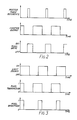
- Figure 2 shows some timing waveforms to go with Figure 1.
- the counter clock and the load clock have been drawn separately in Figure 1 to emphasise that there is no relationship between them. Indeed, if the data input is halted completely, the counters would continue clocking indefinitely, displaying the grey scale image that is stored as phase information.
- the load clock is determined by the picture input rate, while the counter clock is arranged so that the counter recycles above the flicker fusion frequency, for instance, the counter might cycle twice per television field.
- a common sensing line 11 is fed from a tristate driver 12 at each pixel, the tristate driver 12 being active at whichever pixel was last loaded with data. This allows the counter phase to be monitored remotely, which is a check on the operation of the total circuit at that pixel. By continuing to monitor the sensing line, while loading successive counters with data, the operation of each pixel circuit may be checked in turn.
- a counter 2 has one stage more than the number of data bits e.g. for a 4-bit word giving 16 grey levels, the bits are loaded into the four least significant stages of a 5 stage counter.
- a similar counter is used to generate the master phase reference which sets the bi-stable each time the MSB changes, namely every 16 counter clock pulses. If a pixel counter is loaded with a value N and counted down, the M.S.B. changes after N, N+16, N+32 (and so on) clock pulses and re-sets the bi-stable.
- the bi-stable remains in the set state for N clock periods. It is necessary for all the counters using the same master reference phase to be loaded during one period of the counter clock as well as at a specific phase of the master counter.
- the pixel 1 is driven directly by the square wave from the counter output, while the gating is performed by switching on and off the light source.
- Figure 3 shows timing diagrams for this arrangement.
- One advantage is that, as long as the image is static, each pixel 1 is switched on and off for equal times, so has no opportunity to build up a memory of the grey level state it is in.
- a second advantage is that, if the light source can be switched sequentially to red, green, and blue, a colour display can be produced without the need for separate pixels. It is necessary to have separate counters for the red, green, and blue components, so as to control each pixel sequentially, in synchronism with the changes in the light source.
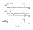
- the pixel drive voltage depends on the display material used, as does the optimum waveform to be used for driving. For instance, if the LCD is of ferroelectric material, the waveform of Figure 2 is not directly suitable, since it contains a d.c. component.
- One solution is to a.c. couple the signal by depositing a thin insulating layer on the display plate to act as a capacitor 20 in series with each ferroelectric liquid crystal device 21 (see Figure 4). The pixel is then switched by the edge spikes of the waveform, assuming that it has a low enough internal resistance to charge up the series capacitor between edges.
- Figure 5 shows the waveforms for this arrangement.
- the back electrode of each pixel is driven directly by the most significant bit of the counter, while the front electrode is driven by the reference square wave.
- the reference square wave has the same frequency as the counter output, but not necessarily the same phase, while its amplitude may be the same or somewhat greater than the amplitude of the counter output. If all the pixels in the image have the same reference square wave, the front of the screen may conveniently be driven as a single electrode.
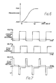
- Figure 6 shows schematically the transmission of a guest-host liquid crystal cell as a function of the rms applied voltage.
- RMS voltages between V1 and V2 are needed to control the cell brightness.
- Figure 7 shows an example of the voltages applied to the electrodes of one LCD pixel according to the invention, together with the voltage across the pixel. As the phase of the back electrode drive is altered the RMS drive across the pixel can in this case be varied between 1 and 6 volts.
- the back electrode square wave is Vb volts rms (2Vb peak to peak) and the front electrode square wave is Vf volts rms
- the rms voltage across the cell can be controlled between (Vf - Vb) and (Vf + Vb).
Landscapes
- Engineering & Computer Science (AREA)
- Chemical & Material Sciences (AREA)
- Crystallography & Structural Chemistry (AREA)
- Physics & Mathematics (AREA)
- Computer Hardware Design (AREA)
- General Physics & Mathematics (AREA)
- Theoretical Computer Science (AREA)
- Multimedia (AREA)
- Signal Processing (AREA)
- Liquid Crystal Display Device Control (AREA)
- Liquid Crystal (AREA)
- Transforming Electric Information Into Light Information (AREA)
Applications Claiming Priority (2)
| Application Number | Priority Date | Filing Date | Title |
|---|---|---|---|
| GB8622714 | 1986-09-15 | ||
| GB868622714A GB8622714D0 (en) | 1986-09-20 | 1986-09-20 | Display device |
Publications (1)
| Publication Number | Publication Date |
|---|---|
| EP0261899A2 true EP0261899A2 (de) | 1988-03-30 |
Family
ID=10604538
Family Applications (1)
| Application Number | Title | Priority Date | Filing Date |
|---|---|---|---|
| EP87308312A Withdrawn EP0261899A2 (de) | 1986-09-20 | 1987-09-18 | Aufzeichnungsvorrichtung |
Country Status (4)
| Country | Link |
|---|---|
| US (1) | US4908613A (de) |
| EP (1) | EP0261899A2 (de) |
| JP (1) | JPS63113497A (de) |
| GB (1) | GB8622714D0 (de) |
Cited By (3)
| Publication number | Priority date | Publication date | Assignee | Title |
|---|---|---|---|---|
| EP1091342A3 (de) * | 1999-10-04 | 2001-12-19 | Matsushita Electric Industrial Co., Ltd. | Technik zur Anzeige einer hohen Anzahl von Graustufen |
| EP1091343A3 (de) * | 1999-09-30 | 2004-09-22 | Agilent Technologies, Inc. (a Delaware corporation) | Digitaler Pixeltreiber mit Graustufensteuerung unter Verwendung von Pulsbreitenmodulation |
| EP1207512A4 (de) * | 2000-03-30 | 2005-10-12 | Seiko Epson Corp | Anzeige |
Families Citing this family (19)
| Publication number | Priority date | Publication date | Assignee | Title |
|---|---|---|---|---|
| US5185602A (en) * | 1989-04-10 | 1993-02-09 | Cirrus Logic, Inc. | Method and apparatus for producing perception of high quality grayscale shading on digitally commanded displays |
| JP2584871B2 (ja) * | 1989-08-31 | 1997-02-26 | キヤノン株式会社 | 表示装置 |
| US5225823A (en) * | 1990-12-04 | 1993-07-06 | Harris Corporation | Field sequential liquid crystal display with memory integrated within the liquid crystal panel |
| DE69226723T2 (de) * | 1991-05-21 | 1999-04-15 | Sharp K.K., Osaka | Verfahren und Einrichtung zum Steuern einer Anzeigeeinrichtung |
| WO1993013513A1 (en) * | 1991-12-24 | 1993-07-08 | Cirrus Logic, Inc. | Process for producing shaded images on display screens |
| US5751265A (en) * | 1991-12-24 | 1998-05-12 | Cirrus Logic, Inc. | Apparatus and method for producing shaded images on display screens |
| JPH06274133A (ja) * | 1993-03-24 | 1994-09-30 | Sharp Corp | 表示装置の駆動回路及び表示装置 |
| US6061039A (en) * | 1993-06-21 | 2000-05-09 | Ryan; Paul | Globally-addressable matrix of electronic circuit elements |
| US5563727A (en) * | 1994-06-30 | 1996-10-08 | Honeywell Inc. | High aperture AMLCD with nonparallel alignment of addressing lines to the pixel edges or with distributed analog processing at the pixel level |
| JP3275991B2 (ja) * | 1994-07-27 | 2002-04-22 | シャープ株式会社 | アクティブマトリクス型表示装置及びその駆動方法 |
| JPH08115060A (ja) * | 1994-10-14 | 1996-05-07 | Sharp Corp | 表示装置の駆動回路及び液晶表示装置 |
| US5751257A (en) | 1995-04-28 | 1998-05-12 | Teletransactions, Inc. | Programmable shelf tag and method for changing and updating shelf tag information |
| US5699074A (en) * | 1995-03-24 | 1997-12-16 | Teletransaction, Inc. | Addressing device and method for rapid video response in a bistable liquid crystal display |
| US6269342B1 (en) | 1995-04-28 | 2001-07-31 | Telxon Corporation | Programmable shelf tag system |
| US6034663A (en) * | 1997-03-10 | 2000-03-07 | Chips & Technologies, Llc | Method for providing grey scale images to the visible limit on liquid crystal displays |
| US6211859B1 (en) | 1997-03-10 | 2001-04-03 | Chips & Technologies, Llc | Method for reducing pulsing on liquid crystal displays |
| WO2000014713A1 (en) * | 1998-09-04 | 2000-03-16 | Fed Corporation | Field sequential reflective liquid crystal display without external frame buffer |
| US7209108B2 (en) * | 2001-11-30 | 2007-04-24 | Avago Technologies Enterprise IP (Singapore) Pte. Ltd. | Differential drive circuit and method for generating an a.c. differential drive signal |
| US20070016460A1 (en) * | 2005-07-14 | 2007-01-18 | Vocollect, Inc. | Task management system having selectively variable check data |
Family Cites Families (4)
| Publication number | Priority date | Publication date | Assignee | Title |
|---|---|---|---|---|
| NL7903515A (nl) * | 1979-05-04 | 1980-11-06 | Philips Nv | Modulatorschakeling voor een matrixweergeefinrichting. |
| US4427978A (en) * | 1981-08-31 | 1984-01-24 | Marshall Williams | Multiplexed liquid crystal display having a gray scale image |
| JPS60158780A (ja) * | 1984-01-27 | 1985-08-20 | Sony Corp | 表示装置 |
| GB8402654D0 (en) * | 1984-02-01 | 1984-03-07 | Secr Defence | Flatpanel display |
-
1986
- 1986-09-20 GB GB868622714A patent/GB8622714D0/en active Pending
-
1987
- 1987-09-18 US US07/098,169 patent/US4908613A/en not_active Expired - Fee Related
- 1987-09-18 EP EP87308312A patent/EP0261899A2/de not_active Withdrawn
- 1987-09-21 JP JP62235069A patent/JPS63113497A/ja active Pending
Cited By (3)
| Publication number | Priority date | Publication date | Assignee | Title |
|---|---|---|---|---|
| EP1091343A3 (de) * | 1999-09-30 | 2004-09-22 | Agilent Technologies, Inc. (a Delaware corporation) | Digitaler Pixeltreiber mit Graustufensteuerung unter Verwendung von Pulsbreitenmodulation |
| EP1091342A3 (de) * | 1999-10-04 | 2001-12-19 | Matsushita Electric Industrial Co., Ltd. | Technik zur Anzeige einer hohen Anzahl von Graustufen |
| EP1207512A4 (de) * | 2000-03-30 | 2005-10-12 | Seiko Epson Corp | Anzeige |
Also Published As
| Publication number | Publication date |
|---|---|
| GB8622714D0 (en) | 1986-10-29 |
| US4908613A (en) | 1990-03-13 |
| JPS63113497A (ja) | 1988-05-18 |
Similar Documents
| Publication | Publication Date | Title |
|---|---|---|
| US4908613A (en) | Display device | |
| US6040815A (en) | LCD drive IC with pixel inversion operation | |
| US5253091A (en) | Liquid crystal display having reduced flicker | |
| EP0351253B1 (de) | Projektionsgerät mit Flüssigkristallen und Steuerverfahren dafür | |
| US5172108A (en) | Multilevel image display method and system | |
| JP2585463B2 (ja) | 液晶表示装置の駆動方法 | |
| JPH07239463A (ja) | アクティブマトリクス型表示装置およびその表示方法 | |
| EP0214857B1 (de) | Verfahren zur Ansteuerung eines Flüssigkristallrasterbildschirmes | |
| US4378557A (en) | Liquid crystal matrix display | |
| EP0489459B1 (de) | Verfahren zum Steuern einer Matrixanzeige und eine durch dieses Verfahren gesteuerte Matrixanzeige | |
| US20040227716A1 (en) | Liquid crystal display and method for operating the same | |
| JPH02135419A (ja) | 液晶表示装置の駆動法 | |
| US5162932A (en) | Method of driving a liquid crystal display with minimum frequency variation of pixel voltage | |
| WO1996010245A1 (en) | Memory configuration for display information | |
| US5541619A (en) | Display apparatus and method of driving display panel | |
| US5298913A (en) | Ferroelectric liquid crystal display device and driving system thereof for driving the display by an integrated scanning method | |
| US4640582A (en) | System for driving a liquid crystal matrix display so as to avoid crosstalk | |
| US7154462B2 (en) | Method and apparatus for driving liquid crystal display | |
| JPS6371889A (ja) | 表示装置の駆動回路 | |
| US4701025A (en) | Liquid crystal display device with driving method to eliminate blur due to frequency dependence | |
| EP0372364B1 (de) | Verfahren und Vorrichtung zum Betrieb einer Anzeige | |
| US5095377A (en) | Method of driving a ferroelectric liquid crystal matrix panel | |
| CA2164803C (en) | Method and circuit for driving picture display devices | |
| JPH08241060A (ja) | 液晶表示装置及びその駆動方法 | |
| JP2891730B2 (ja) | 液晶表示装置と液晶駆動装置 |
Legal Events
| Date | Code | Title | Description |
|---|---|---|---|
| PUAI | Public reference made under article 153(3) epc to a published international application that has entered the european phase |
Free format text: ORIGINAL CODE: 0009012 |
|
| AK | Designated contracting states |
Kind code of ref document: A2 Designated state(s): AT BE CH DE ES FR GB GR IT LI LU NL SE |
|
| STAA | Information on the status of an ep patent application or granted ep patent |
Free format text: STATUS: THE APPLICATION HAS BEEN WITHDRAWN |
|
| 18W | Application withdrawn |
Withdrawal date: 19891106 |
|
| R18W | Application withdrawn (corrected) |
Effective date: 19891106 |
|
| RIN1 | Information on inventor provided before grant (corrected) |
Inventor name: GREEN, IAN MCDONALD |