EP0293156B1 - Abtastungsschaltung - Google Patents
Abtastungsschaltung Download PDFInfo
- Publication number
- EP0293156B1 EP0293156B1 EP88304655A EP88304655A EP0293156B1 EP 0293156 B1 EP0293156 B1 EP 0293156B1 EP 88304655 A EP88304655 A EP 88304655A EP 88304655 A EP88304655 A EP 88304655A EP 0293156 B1 EP0293156 B1 EP 0293156B1
- Authority
- EP
- European Patent Office
- Prior art keywords
- drive voltage
- transistor
- circuit
- drive
- transistors
- Prior art date
- Legal status (The legal status is an assumption and is not a legal conclusion. Google has not performed a legal analysis and makes no representation as to the accuracy of the status listed.)
- Expired - Lifetime
Links
- 208000010152 Huntington disease-like 3 Diseases 0.000 claims description 16
- 201000003570 spinocerebellar ataxia type 17 Diseases 0.000 claims description 13
- 238000000819 phase cycle Methods 0.000 claims 4
- 238000010586 diagram Methods 0.000 description 23
- 239000003990 capacitor Substances 0.000 description 13
- 239000007787 solid Substances 0.000 description 4
- 238000010276 construction Methods 0.000 description 3
- 208000010158 Huntington disease-like 2 Diseases 0.000 description 2
- 239000000969 carrier Substances 0.000 description 2
- 239000000758 substrate Substances 0.000 description 2
- 208000009934 Huntington disease-like 1 Diseases 0.000 description 1
- XUIMIQQOPSSXEZ-UHFFFAOYSA-N Silicon Chemical compound [Si] XUIMIQQOPSSXEZ-UHFFFAOYSA-N 0.000 description 1
- 238000006243 chemical reaction Methods 0.000 description 1
- 230000000694 effects Effects 0.000 description 1
- 238000000034 method Methods 0.000 description 1
- 230000003647 oxidation Effects 0.000 description 1
- 238000007254 oxidation reaction Methods 0.000 description 1
- 230000000630 rising effect Effects 0.000 description 1
- 229910052710 silicon Inorganic materials 0.000 description 1
- 239000010703 silicon Substances 0.000 description 1
Images


Classifications
-
- H—ELECTRICITY
- H10—SEMICONDUCTOR DEVICES; ELECTRIC SOLID-STATE DEVICES NOT OTHERWISE PROVIDED FOR
- H10F—INORGANIC SEMICONDUCTOR DEVICES SENSITIVE TO INFRARED RADIATION, LIGHT, ELECTROMAGNETIC RADIATION OF SHORTER WAVELENGTH OR CORPUSCULAR RADIATION
- H10F39/00—Integrated devices, or assemblies of multiple devices, comprising at least one element covered by group H10F30/00, e.g. radiation detectors comprising photodiode arrays
- H10F39/10—Integrated devices
- H10F39/12—Image sensors
- H10F39/197—Bipolar transistor image sensors
-
- H—ELECTRICITY
- H03—ELECTRONIC CIRCUITRY
- H03K—PULSE TECHNIQUE
- H03K19/00—Logic circuits, i.e. having at least two inputs acting on one output; Inverting circuits
- H03K19/01—Modifications for accelerating switching
- H03K19/017—Modifications for accelerating switching in field-effect transistor circuits
- H03K19/01728—Modifications for accelerating switching in field-effect transistor circuits in synchronous circuits, i.e. by using clock signals
- H03K19/01735—Modifications for accelerating switching in field-effect transistor circuits in synchronous circuits, i.e. by using clock signals by bootstrapping, i.e. by positive feed-back
-
- H—ELECTRICITY
- H03—ELECTRONIC CIRCUITRY
- H03K—PULSE TECHNIQUE
- H03K5/00—Manipulating of pulses not covered by one of the other main groups of this subclass
- H03K5/15—Arrangements in which pulses are delivered at different times at several outputs, i.e. pulse distributors
- H03K5/15013—Arrangements in which pulses are delivered at different times at several outputs, i.e. pulse distributors with more than two outputs
- H03K5/1506—Arrangements in which pulses are delivered at different times at several outputs, i.e. pulse distributors with more than two outputs with parallel driven output stages; with synchronously driven series connected output stages
- H03K5/15093—Arrangements in which pulses are delivered at different times at several outputs, i.e. pulse distributors with more than two outputs with parallel driven output stages; with synchronously driven series connected output stages using devices arranged in a shift register
-
- H—ELECTRICITY
- H04—ELECTRIC COMMUNICATION TECHNIQUE
- H04N—PICTORIAL COMMUNICATION, e.g. TELEVISION
- H04N25/00—Circuitry of solid-state image sensors [SSIS]; Control thereof
- H04N25/70—SSIS architectures; Circuits associated therewith
- H04N25/76—Addressed sensors, e.g. MOS or CMOS sensors
-
- H—ELECTRICITY
- H04—ELECTRIC COMMUNICATION TECHNIQUE
- H04N—PICTORIAL COMMUNICATION, e.g. TELEVISION
- H04N25/00—Circuitry of solid-state image sensors [SSIS]; Control thereof
- H04N25/70—SSIS architectures; Circuits associated therewith
- H04N25/76—Addressed sensors, e.g. MOS or CMOS sensors
- H04N25/779—Circuitry for scanning or addressing the pixel array
-
- H—ELECTRICITY
- H10—SEMICONDUCTOR DEVICES; ELECTRIC SOLID-STATE DEVICES NOT OTHERWISE PROVIDED FOR
- H10F—INORGANIC SEMICONDUCTOR DEVICES SENSITIVE TO INFRARED RADIATION, LIGHT, ELECTROMAGNETIC RADIATION OF SHORTER WAVELENGTH OR CORPUSCULAR RADIATION
- H10F30/00—Individual radiation-sensitive semiconductor devices in which radiation controls the flow of current through the devices, e.g. photodetectors
- H10F30/20—Individual radiation-sensitive semiconductor devices in which radiation controls the flow of current through the devices, e.g. photodetectors the devices having potential barriers, e.g. phototransistors
- H10F30/21—Individual radiation-sensitive semiconductor devices in which radiation controls the flow of current through the devices, e.g. photodetectors the devices having potential barriers, e.g. phototransistors the devices being sensitive to infrared, visible or ultraviolet radiation
- H10F30/24—Individual radiation-sensitive semiconductor devices in which radiation controls the flow of current through the devices, e.g. photodetectors the devices having potential barriers, e.g. phototransistors the devices being sensitive to infrared, visible or ultraviolet radiation the devices having only two potential barriers, e.g. bipolar phototransistors
- H10F30/245—Bipolar phototransistors
Definitions
- the present invention relates to a drive selection circuit that outputs scan pulses in response to drive pulses. It relates in particular to a photosensing pick-up apparatus including such a drive selection circuit.
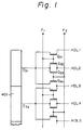
- Fig. 1 is a schematic circuit diagram of a solid state image pickup apparatus using a conventional scan circuit.
- respective output terminals of a scan circuit 401 are connected to horizontal lines HDL1, HDL2, and HDL3, and to horizontal lines HDL3, HDL4, HDL5, ...through transistors Qy1 to Qy4.
- a signal F1 to select odd number fields is input to gate electrodes of the transistors Qy1 and Qy2.
- a signal F2 to select even number fields is input to gate electrodes of the transistors Qy3 and Qy4. Namely, the transistors Qy1 to Qy4 constitute an interlacing circuit.
- scan pulses Oy1, Oy2, ... are sequentially output to the horizontal lines HDL1 and HDL2, horizontal lines HDL3, and HDL4, ... through the transistors Qy1 and Qy2.
- the scan pulses 0y1, Oy2, ... are sequentially output to the horizontal lines HDL2 and HDL3, the HDL4, and HDL5, ... through the transistors Qy3 and Qy4.
- the signals Oy1 and Oy2 are transferred to the horizontal lines HDL through the transistors Qy1 and Qy2 and the transistors Qy3 and Qy4 of the interlacing circuit. Therefore, there are problems such that a voltage drop due to a threshold value voltage Vth of the transistor Qy occurs and the dynamic range is narrowed, so that the picture quality deteriorates.
- the conventional drive circuit cannot be used in the image pickup devices in which a signal is readout by every one vertical line. Namely, the conventional constitution has problems such that there is a limitation in driving manner and this constitution can be applied to only the limited driving method.
- a drive selection circuit which can support various kinds of driving modes such as interlacing scan, non-interlacing scan and the like is needed.
- a drive selection circuit that outputs scan pulses, said circuit comprising: a ripple shift register having a plurality of output stages; and a switch array including a plurality of first transistors and a plurality of second transistors, wherein: each first transistor and each second transistor has a gate connected to a common respective output stage of said ripple-shift register; said first transistors are each connected between a common first drive voltage line and a respective selection line output of said switch array; and said second transistors are each connected between a common second drive voltage line and a respective selection line output of said switch array; which circuit is characterised by: a plurality of third transistors each having a gate connected to said common respective output stage, and each said third transistor being connected between a common third drive voltage line and the respective selection line output which is connected to that first transistor the gate of which is connected to the next output stage, of said ripple-shift register.
- each line can be independently driven and various kinds of driving modes such as interlacing scan, non-interlacing scan, and the like of a plurality of lines can be easily realised.
- Fig. 2A is a partial circuit diagram of a first example of ripple shift register and Fig. 2B is a voltage waveform diagram for explaining its operation.
- n unit circuits are provided and scan pulses ⁇ 1 to ⁇ n are sequentially output from these unit circuits.
- the potential of each section in Fig. 2A is expressed as V(i) where the reference number (i) identifies the corresponding unit circuit.
- a transistor M1 in the first unit circuit when a pulse 0v1 rises after a P s has been applied, a transistor M1 is made conductive and a potential V(4) rises. Since the potential V(4) is the gate potential of a transistor M2, the transistor M2 shows a conductance corresponding to the potential V(4).
- the potential V(5) increases through the transistor M2.
- the increase in the potential V(5) is fed back to a gate of the transistor M2 via a capacitor C1, thereby increasing the potential V(4) due to a bootstrap effect.
- the increase in the potential V(4) acts so as to raise the conductance of the transistor M2. Therefore, the pulse ⁇ v2 passes, while a voltage drop hardly occurs due to the transistor M2. This pulse is transmitted through a transistor M3, thereby increasing the potential V(6).
- the potential V(6) is the gate potential of a transistor M6, a conductance of the transistor M6 rises in correspondence to the potential V(6).
- the pulse ⁇ v1 When the pulse ⁇ v1 subsequently rises, the potential V(7) increases through the transistor M6. The potential V(6) further rises due to the increase in the potential V(7). Since the increase in the potential V(6) acts so as to enhance the conductance of the transistor M6, the pulse ⁇ v1 allows the potential V(8) to be raised through the transistors M6 and M7 (refer to Fig. 2B). Therefore, a transistor M10 exhibits the conductance corresponding to the gate potential V(8).
- the potential V(8) is reset by the pulse ⁇ v1 and at the same time, the potential V(12) rises and, further, increases by the subsequent pulse ⁇ v2 .
- the potential V(12) is used as a scan pulse ⁇ 2.
- scan pulses ⁇ 3 to ⁇ n at a high voltage level are successively output synchronously with the pulses ⁇ v2 .
- Fig. 3 is a partial circuit diagram of another construction of ripple shift register which can be adapted.
- Fig. 4 is a voltage waveform diagram for explaining the operation thereof.
- a transistor M1 is turned on and a potential V(A) rises by a start pulse P s and a drive pulse ⁇ v1 .
- Transistors M2 and M3 conduct.
- the scan pulse at a high voltage can be derived in a manner similar to the first example.
- scan pulses ⁇ 2 to ⁇ n at a high voltage level can be successively output synchronously with the drive pulses ⁇ v1 and ⁇ v2 .
- Fig. 5 is a schematic circuit diagram of a photosensitive image pickup apparatus including the ripple shift register just described.
- Fig. 6 is a timing chart for explaining the operation thereof.
- this image pickup apparatus comprises photoelectric converting cells C11, C12, ... which are arranged in a two-dimensional array and driven each row by each one of several horizontal lines HDL1, HDL2, HDL3, ... Photoelectric conversion signals are read out through vertical lines and transistors Q1 and Q2.
- gate electrodes of three transistors Q v1 to Q v3 are connected to the output terminals of a scan circuit 101, respectively.
- Each transistor Q v1 transfers a drive voltage V r1 to a respective one of each of the horizontal lines HDL1, HDL3, HDL5, ....
- Each transistor Q v2 transfers a drive voltage V r2 to a respective one of each of the horizontal lines HDL2, HDL4, HDL6, ....
- Each respective transistor Q v3 transfers a drive voltage V r3 to the respective horizontal line HDL3, HDL5, HDL7, ....
- the scan circuit 101 sequentially outputs the scan pulses ⁇ 1, ⁇ 2, ... in response to pulses ⁇ v1 and ⁇ v2 . Therefore, by applying the drive voltages V r1 to V r3 by a proper combination, the image pickup device can be scanned in a desired mode.
- the horizontal lines HDL1 and HDL2, and HDL3 and HDL4, ... are driven and by applying the drive voltage V r2 and V r3 in the even number fields, the HDL2 and HDL3, and HDL4 and HDL5, ... are driven.
- the interlacing scan of the two line driving type can be accomplished.
- the vertical line of the image pickup device can be also set to a single vertical line.
- the output of the scan circuit 101 can be set to a high voltage level, and the transistors Q v1 to Q v3 can be set to a sufficient high conductance
- the drive voltages V r1 to V r3 can be transferred to the horizontal lines HDL without having to reduce the drive voltages V r1 to V r3 .
- Fig. 7 is a schematic circuit diagram of another example of apparatus.
- Fig. 8 is a timing chart for explaining the operation thereof.
- the interlacing scan of the three-line driving type can be also accomplished.
- Fig. 9 is a schematic cross sectional view of a photoelectric converting cell which can be used in the solid state image pickup apparatus just described.
- an n ⁇ layer 202 serving as a collector region is formed on an n type silicon substrate 201 by the epitaxial growth.
- a p base region 203 is formed in the n ⁇ layer 202.
- An n+ emitter region 204 is further formed in the p base region 203. In this manner, a bipolar transistor is constituted.
- the p base region 203 is two-dimensionally arranged.
- the cells in the horizontal direction are separated from the cells in the vertical direction by a device separating region.
- the device separating region comprises an oxide film formed by the LOCOS oxidation and an n+ region formed under the oxide film.
- a gate electrode 208 is formed between horizontally neighboring p base regions 203 through an oxide film 207. Therefore, a p channel MOS transistor Q c in which the adjacent p base regions 203 are used as source and drain regions is constituted.
- This MOS transistor is the normally OFF type and is set to the OFF state when the potential of the gate electrode 208 is the earth potential or positive potential. Therefore, the p base regions 203 between the adjacent cells are electrically isolated. On the contrary, when the potential of the gate electrode 208 is a negative potential which exceeds a threshold value potential V th , the MOS transistor is set to the ON state, so that the p base regions 203 of the respective cells are mutually made conductive.
- the gate electrodes 208 are commonly connected to the drive line every row in the horizontal direction. Further, capacitors 209 to control the potentials of the p base regions 203 are also similarly connected to the drive line.
- the drive line extends in the horizontal direction on the oxide film serving as the device separating region.
- an emitter electrode 212 is formed.
- the emitter electrodes 212 are connected to a vertical line 213 every column.
- a collector electrode 214 is formed on the back surface of the substrate 201 through an ohmic contact layer.
- Fig. 10A is an equivalent circuit diagram of the photoelectric converting cell.
- Fig. 10B is a voltage waveform diagram for explaining the operation thereof.
- pulses ⁇ d of a positive voltage are applied to a drive line 210 for only a period of time T rd .
- the potential of the p base region 203 rises through a capacitor C ox and the signal is read out to the emitter electrode 212 as mentioned above.
- pulses ⁇ d of a negative voltage are applied to the drive line 210 for only a period of time T rh .
- the p channel MOS transistor Q c is turned on and the base potential is reset to the voltage V c and the resetting operation is completed
- the transistor Q r is turned on, thereby resetting the vertical line 213.
- the pulse ⁇ d of a positive voltage can be also applied while the emitter electrode 212 is grounded. In this case, there is no need to set the voltage V c to a negative voltage but can be set to the earth voltage or positive voltage.
- Fig. 11 is a schematic circuit diagram of an image pickup apparatus using the foregoing photoelectric converting cell.
- m x n photoelectric converting cells are arranged as a two dimensional array.
- the gate electrodes 208 of the MOS transistor Q c are commonly connected to the drive lines HDL1 to HDL m , respectively.
- the drive lines HDL1 to HDL m are connected to a vertical buffer circuit 301.
- the scan pulses ⁇ 1 to ⁇ m are input to the vertical buffer circuit 301 from the vertical scan circuit 101,
- MOS transistors Q c in each of which the p base regions 203 in each cell are used as source and drain regions are serially connected every horizontal line.
- the p regions to form the MOS transistor Q c are respectively formed in the cells C11 to C m1 arranged at the edge line.
- MOS transistors Q xl to Q xm are respectively serially connected to the cells C 1n to C mn .
- a constant voltage V c is applied to both ends.
- the emitter electrodes in the cells C11 to C m1 , C12 to C m2 , ... in the vertical direction are commonly connected to vertical lines VL1 to VL n , respectively.
- the vertical lines are grounded through reset transistors Q r1 to Q rn .
- a reset pulse ⁇ r is commonly input to the gate electrodes of the transistors Q r1 to Q rn .
- the vertical lines VL1 to VL n are connected to capacitors C1 and C2 through transistors Q t1 and Q t2 , respectively.
- the pulses ⁇ 1 and ⁇ 2 are input to the gate electrodes of the transistors Q t1 and Q t2 .
- capacitors C1 and C2 are connected to signal lines 303 and 304 through the transistors Q1 and Q2, respectively.
- Scan pulses ⁇ 11 to ⁇ n1 of a horizontal scan circuit 302 are input to the gate electrodes of the transistors Q1 and Q2, respectively.
- Various kinds of pulses ⁇ , voltages V, and the like to drive the image pickup apparatus are supplied from a driver 305.
- the driver 305 is controlled by a controller 306.
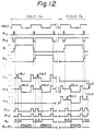
- Fig. 12 is a timing chart for schematically explaining the operation of the image pickup apparatus.
- the scan pulse ⁇ 1 rises.
- the scan pulse ⁇ 1 is set to a high voltage.
- the vertical buffer circuit 301 outputs input voltages V r1 and V r2 to the horizontal lines HDL1 and HDL2, respectively.
- the pulses ⁇ t1 and ⁇ r rise and the transfer transistor Q t1 and reset transistor Q r are turned on, thereby clearing the vertical lines VL and capacitor C1.
- the input voltage V r1 is set to a positive voltage and the reading operations of the cells C11 to C 1n on the horizontal line HDL1 are executed.
- the readout signals are stored into the capacitor C1 through the transfer transistor Q t1 , respectively.
- the input V r2 is set to a positive voltage and the reading operations of the cells C21 to C 2n on the horizontal line HDL2 are executed.
- the readout signals are stored into the capacitor C2 through the transfer transistor Q t2 .
- the transistors Q1 and Q2 are sequentially turned on by the scan pulses ⁇ 11 to ⁇ n1 which are successively output from the horizontal scan circuit 302.
- the signals stored in the capacitors C1 and C2 are read out and output to the signal lines 303 and 304.
- the pulse ⁇ r rises and the transistor Q r is turned on, thereby grounding the vertical lines VL.
- the input voltages V r1 and V r2 are set to a negative voltage, thereby resetting the cells of the first and second rows. That is, the MOS transistor Q c of each cell are turned on and each base potential is set to a common potential.
- the input voltages V r1 and V r2 are set to a positive voltage, thereby resetting the base regions 203 which were reset to a common potential.
- the emitter electrodes of the cells are grounded through the vertical lines VL, when a positive voltage is applied to capacitors C ox , the circuit between the base and emitter is forwardly biased, so that the carriers accumulated in the base region 203 are extinguished in a manner similar to the reading operations.
- the cells of the first and second rows start the accumulating operation.
- the reading and resetting operations of the third and fourth rows, the fifth and sixth rows, ... in the odd number fields F o are sequentially executed by the pulses ⁇ v1 and ⁇ v2 .
- drive signals are supplied to the drive lines in a desired mode on the basis of the scan output of the scan circuit and a desired combination of the drive signals, even when a plurality of drive lines are scanned, they can be independently driven.
- Various kinds of driving modes such as interlacing scan, non-interlacing scan, and the like of a plurality of lines can be easily performed.
Landscapes
- Engineering & Computer Science (AREA)
- Physics & Mathematics (AREA)
- Multimedia (AREA)
- Signal Processing (AREA)
- Computer Hardware Design (AREA)
- Computing Systems (AREA)
- General Engineering & Computer Science (AREA)
- Mathematical Physics (AREA)
- Nonlinear Science (AREA)
- Transforming Light Signals Into Electric Signals (AREA)
Claims (5)
- Treiberauswahlschaltung (301), die Abtastimpulse ausgibt, mit:
einem Wellen-Schieberegister (101) mit einer Vielzahl von Ausgangsstufen (φ₁, φ₂, φ₃); und
einem Schalterfeld (Qv1 bis Qv3) mit einer Vielzahl von ersten Transistoren (Qv1) und einer Vielzahl von zweiten Transistoren (Qv2), wobei:
jeder erste Transistor (Qv1) und jeder zweite Transistor (Qv2) ein mit einer jeweils gemeinsamen Ausgangsstufe (φ₁, φ₂, φ₃, ...) des Wellen-Schieberegisters (101) verbundenes Gate besitzt; jeder der ersten Transistoren (Qv1) zwischen einer gemeinsamen ersten Treiberspannungsleitung (Vr1) und einem jeweiligen Auswahlleitungsausgang (HDL1, HDL3, HDL5, ...) des Schalterfelds (Qv1 bis Qv3) verbunden ist; und
jeder der zweiten Transistoren (Qv2) zwischen einer gemeinsamen zweiten Treiberspannungsleitung (Vr₂) und einem jeweiligen Auswahlleitungsausgang (HDL2, HDL4, HDL6, ...) des Schalterfelds (Qv1 bis Qv3) verbunden ist;
wobei die Treiberauswahlschaltung gekennzeichnet ist durch:
eine Vielzahl von dritten Transistoren (Qv3), von denen jeder ein mit der jeweils gemeinsamen Ausgangsstufe (φ₁, φ₂, φ₃, ...) verbundenes Gate besitzt, und jeder der dritten Transistoren (Qv3) zwischen einer gemeinsamen dritten Treiberspannungsleitung (Vr3) und dem jeweiligen Auswahlleitungsausgang (HDL3, HDL5, ...) verbunden ist, der mit dem ersten Transistor (Qv1) verbunden ist, dessen Gate mit der nächsten Ausgangsstufe (φ₂, φ₃) des Wellen-Schieberegisters (101) verbunden ist. - Schaltung gemäß Anspruch 1, gekennzeichnet durch:
eine Treiberspannungsquelle (305), die mit der ersten, zweiten und dritten Treiberspannungsleitung (Vr1, Vr2, Vr3) jeweils zum Anlegen von ersten, zweiten, und dritten Treibspannungssignalen (Vr1, Vr2, Vr3) verbunden ist,
wobei die Treiberspannungsquelle (305) derart betriebsfähig ist, daß für ein ungerades Feld die ersten und zweiten Treiberspannungssignale (Vr1, Vr2) aus jeweils gleichphasigen Folgen von regelmäßigen Impulsen (HDL1, HDL3, HDL5; HDL2, HDL4, HDL6) bestehen, während das dritte Treiberspannungssignal (Vr3) in Ruhe ist, und, daß für ein gerades Feld das erste Treiberspannungssignal (Vr1) in Ruhe ist, während die zweiten und dritten Treiberspannungssignale (Vr2, Vr3) aus jeweils gleichphasigen Folgen von regelmäßigen Impulsen (HDL2, HDL4, HDL6; HDL3, HDL5, HDL7) bestehen. - Schaltung gemäß Anspruch 1,
gekennzeichnet durch
eine Vielzahl von vierten Transistoren (Qv4), von denen jeder ein mit der jeweils gemeinsamen Ausgangsstufe (φ₁, φ₂, φ₃, ...) verbundenes Gate besitzt, und jeder vierte Transistor (Qv4) zwischen einer gemeinsamen vierten Treiberspannungsleitung (Vr4) und dem jeweiligen Auswahlausgang (HDL4, HDL6, HDL8, ...) verbunden ist, der mit dem zweiten Transistor (Qv2) verbunden ist, dessen Gate mit der nächsten Ausgangsstufe (φ₂, φ₃, ...) des Wellen-Schieberegisters (101) verbunden ist. - Schaltung gemäß Anspruch 3, gekennzeichnet durch
eine Treiberspannungsquelle (305), die mit der ersten, zweiten, dritten und vierten Treiberspannungsleitung (Vr1, Vr2, Vr3, Vr4) jeweils zum Anlegen von ersten, zweiten, dritten und vierten Treiberspannungssignalen (Vr1, Vr2, Vr3, Vr4) verbunden ist,
wobei die Treiberspannungsquelle (305) derart betriebsfähig ist, daß für ein ungerades Feld die ersten, zweiten und dritten Treiberspannungssignale (Vr1, Vr2, Vr3) aus jeweils gleichphasigen Folgen von regelmäßigen Impulsen (HDL1, HDL3, HDL5; HDL2, HDL4, HDL6; HDL3, HDL5, HDL7) bestehen, während das vierte Treiberspannungssignal (Vr4) in Ruhe ist, und daß für ein gerades Feld das erste Treiberspannungssignal (Vr1) in Ruhe ist, während die zweiten, dritten und vierten Treiberspannungssignale (Vr2, Vr3, Vr4) aus gleichphasigen Folgen von regelmäßigen Impulsen (HDL2, HDL4, HDL6; HDL3; HDL5, HDL7; HDL4, HDL6, HDL8) bestehen. - Lichtempfindliche Aufnahmevorrichtung mit:
einem in Zeilen und Spalten angeordneten Feld von Photozellen (C₁₁ bis Cmn);
einer Vielzahl von Auswahlleitungen (HDL1, ..., HDLm), von denen jede mit einer jeweiligen Reihe (C₁₁ bis C1n, ..., Cm1 bis Cmn) der Photozellen (C₁₁ bis Cmn) verbunden ist;
einer Treiberauswahlschaltung (301) gemäß Anspruch 1, deren Auswahlleitungsausgänge (HDL1 bis HDLm) mit den jeweiligen Auswahlleitungen (HDL1 bis HDLm) verbunden sind;
einer an das Wellen-Schieberegister (101) der Treiberauswahlschaltung angeschlossenen ersten Signalquelle (305) zum Zuführen von Synchronisations- und Taktgeberschiebesteuersignalen (φVS, φV1, φV2) zum Abtasten der Auswahlleitungen (HDL1 bis HDLM); und
einer mit den gemeinsamen Treiberspannungsleitungen (Vr1 bis Vr3; Vr1 bis Vr4) des Schalterfelds der Treiberauswahlschaltung verbundenen zweiten Signalquelle (305) zum Zuführen von Treiberspannungssignalen (Vr1 bis Vr3; Vr1 bis Vr3).
Applications Claiming Priority (4)
| Application Number | Priority Date | Filing Date | Title |
|---|---|---|---|
| JP62125925A JP2559407B2 (ja) | 1987-05-25 | 1987-05-25 | 走査回路 |
| JP125926/87 | 1987-05-25 | ||
| JP125925/87 | 1987-05-25 | ||
| JP62125926A JP2635966B2 (ja) | 1987-05-25 | 1987-05-25 | 撮像装置 |
Publications (3)
| Publication Number | Publication Date |
|---|---|
| EP0293156A2 EP0293156A2 (de) | 1988-11-30 |
| EP0293156A3 EP0293156A3 (en) | 1989-09-06 |
| EP0293156B1 true EP0293156B1 (de) | 1994-07-27 |
Family
ID=26462224
Family Applications (1)
| Application Number | Title | Priority Date | Filing Date |
|---|---|---|---|
| EP88304655A Expired - Lifetime EP0293156B1 (de) | 1987-05-25 | 1988-05-23 | Abtastungsschaltung |
Country Status (3)
| Country | Link |
|---|---|
| US (2) | US4922138A (de) |
| EP (1) | EP0293156B1 (de) |
| DE (1) | DE3850811T2 (de) |
Families Citing this family (24)
| Publication number | Priority date | Publication date | Assignee | Title |
|---|---|---|---|---|
| DE69033613T2 (de) * | 1989-05-31 | 2001-05-03 | Canon K.K., Tokio/Tokyo | Fotoelektrischer Umwandler |
| KR920000403B1 (ko) * | 1989-09-23 | 1992-01-13 | 현대전자산업 주식회사 | 개선된 붙스트래핑 레벨 조정회로 |
| US5410349A (en) * | 1990-07-06 | 1995-04-25 | Fuji Photo Film Co., Ltd. | Solid-state image pick-up device of the charge-coupled device type synchronizing drive signals for a full-frame read-out |
| IT1244205B (it) * | 1990-12-19 | 1994-07-08 | Sgs Thomson Microelectronics | Circuito di generazione di un clock di scansione in un dispositivo di analisi operativa di tipo seriale per circuito integrato |
| US5153467A (en) * | 1991-06-12 | 1992-10-06 | Etron Technology, Inc. | Bootstrap circuit for word line driver in semiconductor memory |
| JP3189990B2 (ja) * | 1991-09-27 | 2001-07-16 | キヤノン株式会社 | 電子回路装置 |
| DE69311930T2 (de) * | 1992-01-31 | 1997-11-20 | Canon Kk | Flüssigkristall-Lichtventil mit aktiver Matrix und Treiberschaltung |
| US5406332A (en) * | 1992-03-06 | 1995-04-11 | Canon Kabushiki Kaisha | Photoelectric converting device |
| US5617531A (en) * | 1993-11-02 | 1997-04-01 | Motorola, Inc. | Data Processor having a built-in internal self test controller for testing a plurality of memories internal to the data processor |
| JP3385760B2 (ja) * | 1994-02-21 | 2003-03-10 | ソニー株式会社 | 固体撮像装置及びその駆動方法 |
| US5592493A (en) * | 1994-09-13 | 1997-01-07 | Motorola Inc. | Serial scan chain architecture for a data processing system and method of operation |
| US5883608A (en) * | 1994-12-28 | 1999-03-16 | Canon Kabushiki Kaisha | Inverted signal generation circuit for display device, and display apparatus using the same |
| JP3529190B2 (ja) * | 1995-04-03 | 2004-05-24 | オリンパス株式会社 | 固体撮像装置 |
| GB9614480D0 (en) * | 1995-12-01 | 1996-09-04 | Philips Electronics Nv | Multiplexer circuit |
| GB2343309A (en) * | 1998-10-27 | 2000-05-03 | Sharp Kk | Clock pulse generator for LCD |
| JP3910765B2 (ja) * | 1999-09-08 | 2007-04-25 | 株式会社東芝 | 電圧発生回路及びこれを用いた電圧転送回路 |
| US20030052848A1 (en) * | 2001-09-20 | 2003-03-20 | Matsushita Electric Industrial Co., Ltd | Signal transmission circuit, solid-state imaging device, camera and liquid crystal display |
| JP4387684B2 (ja) * | 2003-04-04 | 2009-12-16 | パナソニック株式会社 | 固体撮像装置、その駆動方法及びカメラ |
| JP4337779B2 (ja) * | 2004-07-01 | 2009-09-30 | ソニー株式会社 | 物理情報取得方法および物理情報取得装置並びに物理量分布検知の半導体装置 |
| KR20070091767A (ko) * | 2006-03-07 | 2007-09-12 | 삼성에스디아이 주식회사 | 플라즈마 디스플레이 패널의 구동장치 |
| US7920668B2 (en) * | 2007-01-05 | 2011-04-05 | Chimei Innolux Corporation | Systems for displaying images by utilizing vertical shift register circuit to generate non-overlapped output signals |
| US9076756B2 (en) | 2010-09-02 | 2015-07-07 | Sharp Kabushiki Kaisha | Semiconductor device, semiconductor device unit, active matrix substrate, liquid crystal panel, and liquid crystal display |
| JP5730030B2 (ja) * | 2011-01-17 | 2015-06-03 | 浜松ホトニクス株式会社 | 固体撮像装置 |
| JP6478488B2 (ja) | 2014-06-18 | 2019-03-06 | キヤノン株式会社 | Ad変換装置及び固体撮像装置 |
Family Cites Families (11)
| Publication number | Priority date | Publication date | Assignee | Title |
|---|---|---|---|---|
| JPS5631790B2 (de) * | 1971-12-22 | 1981-07-23 | ||
| GB1459951A (en) * | 1974-07-25 | 1976-12-31 | Integrated Photomatrix Ltd | Shift registers |
| JPS585627B2 (ja) * | 1977-08-10 | 1983-02-01 | 株式会社日立製作所 | 固体撮像装置 |
| FR2405513A1 (fr) * | 1977-10-07 | 1979-05-04 | Cii Honeywell Bull | Circuit generateur de phase de commande d'execution d'operations dans un systeme informatique |
| JPS54161288A (en) * | 1978-06-12 | 1979-12-20 | Hitachi Ltd | Semiconductor device |
| US4316106A (en) * | 1980-01-11 | 1982-02-16 | Mostek Corporation | Dynamic ratioless circuitry for random logic applications |
| JPS6045512B2 (ja) * | 1980-03-05 | 1985-10-09 | 株式会社東芝 | ダイナミック型シフトレジスタ回路 |
| JPS5945696A (ja) * | 1982-09-08 | 1984-03-14 | Sony Corp | 信号伝送回路 |
| NL192315C (nl) * | 1983-01-18 | 1997-05-07 | Philips Electronics Nv | Televisiecamera uitgevoerd met een vaste stof opneeminrichting. |
| JPS6161586A (ja) * | 1984-08-31 | 1986-03-29 | Olympus Optical Co Ltd | カラ−撮像装置の照明装置 |
| JP2656475B2 (ja) * | 1986-10-01 | 1997-09-24 | 株式会社日立製作所 | 固体撮像装置 |
-
1988
- 1988-05-20 US US07/196,479 patent/US4922138A/en not_active Expired - Lifetime
- 1988-05-23 EP EP88304655A patent/EP0293156B1/de not_active Expired - Lifetime
- 1988-05-23 DE DE3850811T patent/DE3850811T2/de not_active Expired - Fee Related
-
1990
- 1990-02-07 US US07/476,528 patent/US5119202A/en not_active Expired - Lifetime
Also Published As
| Publication number | Publication date |
|---|---|
| EP0293156A3 (en) | 1989-09-06 |
| EP0293156A2 (de) | 1988-11-30 |
| DE3850811T2 (de) | 1994-12-15 |
| DE3850811D1 (de) | 1994-09-01 |
| US4922138A (en) | 1990-05-01 |
| US5119202A (en) | 1992-06-02 |
Similar Documents
| Publication | Publication Date | Title |
|---|---|---|
| US5119202A (en) | Scan circuit with bootstrap drive | |
| US4835404A (en) | Photoelectric converting apparatus with a switching circuit and a resetting circuit for reading and resetting a plurality of lines sensors | |
| US4959723A (en) | Solid state image pickup apparatus having multi-phase scanning pulse to read out accumulated signal | |
| US5172249A (en) | Photoelectric converting apparatus with improved switching to reduce sensor noises | |
| EP0272152B1 (de) | Signalausleseschaltung | |
| US4810896A (en) | Photoelectric conversion device with reduced fixed pattern noises | |
| EP0455311B1 (de) | Bildsensoranordnung | |
| US3919468A (en) | Charge transfer circuits | |
| US4212034A (en) | Solid-state image pickup device | |
| US6049357A (en) | Image pickup apparatus including signal accumulating cells | |
| EP0055592A2 (de) | Festkörper-Bildaufnahmevorrichtung | |
| EP0576022A1 (de) | Photoelektrischer Wandler und Steuerverfahren dafür | |
| US4626916A (en) | Solid state image pickup device | |
| US4055836A (en) | Charge transfer readout circuits | |
| JPH084129B2 (ja) | 光電変換装置 | |
| US5262850A (en) | Photoelectric converting device having reduced line sensor space | |
| US5825056A (en) | Scanning switch transistor for solid state imaging device | |
| US5831675A (en) | Solid state imaging device | |
| US5483283A (en) | Three level high speed clock driver for an image sensor | |
| JP2559407B2 (ja) | 走査回路 | |
| JP2635966B2 (ja) | 撮像装置 | |
| US7471326B2 (en) | Scanning switch transistor for solid-state imaging device | |
| JP2589312B2 (ja) | 光電変換装置 | |
| JP2598103B2 (ja) | 光電変換装置 | |
| JPH0697408A (ja) | 光電変換装置及びその製造方法 |
Legal Events
| Date | Code | Title | Description |
|---|---|---|---|
| PUAI | Public reference made under article 153(3) epc to a published international application that has entered the european phase |
Free format text: ORIGINAL CODE: 0009012 |
|
| AK | Designated contracting states |
Kind code of ref document: A2 Designated state(s): DE FR GB IT NL |
|
| PUAL | Search report despatched |
Free format text: ORIGINAL CODE: 0009013 |
|
| AK | Designated contracting states |
Kind code of ref document: A3 Designated state(s): DE FR GB IT NL |
|
| 17P | Request for examination filed |
Effective date: 19900124 |
|
| 17Q | First examination report despatched |
Effective date: 19900921 |
|
| GRAA | (expected) grant |
Free format text: ORIGINAL CODE: 0009210 |
|
| AK | Designated contracting states |
Kind code of ref document: B1 Designated state(s): DE FR GB IT NL |
|
| PG25 | Lapsed in a contracting state [announced via postgrant information from national office to epo] |
Ref country code: IT Free format text: LAPSE BECAUSE OF FAILURE TO SUBMIT A TRANSLATION OF THE DESCRIPTION OR TO PAY THE FEE WITHIN THE PRE;WARNING: LAPSES OF ITALIAN PATENTS WITH EFFECTIVE DATE BEFORE 2007 MAY HAVE OCCURRED AT ANY TIME BEFORE 2007. THE CORRECT EFFECTIVE DATE MAY BE DIFFERENT FROM THE ONE RECORDED.SCRIBED TIME-LIMIT Effective date: 19940727 Ref country code: FR Effective date: 19940727 Ref country code: NL Effective date: 19940727 |
|
| REF | Corresponds to: |
Ref document number: 3850811 Country of ref document: DE Date of ref document: 19940901 |
|
| EN | Fr: translation not filed | ||
| NLV1 | Nl: lapsed or annulled due to failure to fulfill the requirements of art. 29p and 29m of the patents act | ||
| PLBE | No opposition filed within time limit |
Free format text: ORIGINAL CODE: 0009261 |
|
| STAA | Information on the status of an ep patent application or granted ep patent |
Free format text: STATUS: NO OPPOSITION FILED WITHIN TIME LIMIT |
|
| 26N | No opposition filed | ||
| REG | Reference to a national code |
Ref country code: GB Ref legal event code: IF02 |
|
| PGFP | Annual fee paid to national office [announced via postgrant information from national office to epo] |
Ref country code: GB Payment date: 20060517 Year of fee payment: 19 |
|
| PGFP | Annual fee paid to national office [announced via postgrant information from national office to epo] |
Ref country code: DE Payment date: 20060726 Year of fee payment: 19 |
|
| GBPC | Gb: european patent ceased through non-payment of renewal fee |
Effective date: 20070523 |
|
| PG25 | Lapsed in a contracting state [announced via postgrant information from national office to epo] |
Ref country code: DE Free format text: LAPSE BECAUSE OF NON-PAYMENT OF DUE FEES Effective date: 20071201 |
|
| PG25 | Lapsed in a contracting state [announced via postgrant information from national office to epo] |
Ref country code: GB Free format text: LAPSE BECAUSE OF NON-PAYMENT OF DUE FEES Effective date: 20070523 |