EP0282370A2 - Dynamische logische Anordnung - Google Patents
Dynamische logische Anordnung Download PDFInfo
- Publication number
- EP0282370A2 EP0282370A2 EP88400303A EP88400303A EP0282370A2 EP 0282370 A2 EP0282370 A2 EP 0282370A2 EP 88400303 A EP88400303 A EP 88400303A EP 88400303 A EP88400303 A EP 88400303A EP 0282370 A2 EP0282370 A2 EP 0282370A2
- Authority
- EP
- European Patent Office
- Prior art keywords
- matrix
- phase
- logic
- transistor
- transistors
- Prior art date
- Legal status (The legal status is an assumption and is not a legal conclusion. Google has not performed a legal analysis and makes no representation as to the accuracy of the status listed.)
- Granted
Links
- 239000011159 matrix material Substances 0.000 claims abstract description 103
- 238000002955 isolation Methods 0.000 claims abstract description 29
- 230000036316 preload Effects 0.000 claims abstract description 10
- 230000005669 field effect Effects 0.000 claims description 16
- 230000000295 complement effect Effects 0.000 claims description 12
- 230000000694 effects Effects 0.000 claims description 2
- 230000005764 inhibitory process Effects 0.000 claims 2
- 238000005516 engineering process Methods 0.000 abstract description 2
- 238000004519 manufacturing process Methods 0.000 abstract description 2
- 238000010586 diagram Methods 0.000 description 14
- 230000010354 integration Effects 0.000 description 3
- 230000003068 static effect Effects 0.000 description 3
- 210000000352 storage cell Anatomy 0.000 description 2
- 230000003321 amplification Effects 0.000 description 1
- 230000000903 blocking effect Effects 0.000 description 1
- 239000004020 conductor Substances 0.000 description 1
- 230000009977 dual effect Effects 0.000 description 1
- 235000021183 entrée Nutrition 0.000 description 1
- 238000009413 insulation Methods 0.000 description 1
- 238000003199 nucleic acid amplification method Methods 0.000 description 1
- 238000010200 validation analysis Methods 0.000 description 1
Images

Classifications
-
- H—ELECTRICITY
- H03—ELECTRONIC CIRCUITRY
- H03K—PULSE TECHNIQUE
- H03K19/00—Logic circuits, i.e. having at least two inputs acting on one output; Inverting circuits
- H03K19/02—Logic circuits, i.e. having at least two inputs acting on one output; Inverting circuits using specified components
- H03K19/173—Logic circuits, i.e. having at least two inputs acting on one output; Inverting circuits using specified components using elementary logic circuits as components
- H03K19/177—Logic circuits, i.e. having at least two inputs acting on one output; Inverting circuits using specified components using elementary logic circuits as components arranged in matrix form
- H03K19/17704—Logic circuits, i.e. having at least two inputs acting on one output; Inverting circuits using specified components using elementary logic circuits as components arranged in matrix form the logic functions being realised by the interconnection of rows and columns
- H03K19/17708—Logic circuits, i.e. having at least two inputs acting on one output; Inverting circuits using specified components using elementary logic circuits as components arranged in matrix form the logic functions being realised by the interconnection of rows and columns using an AND matrix followed by an OR matrix, i.e. programmable logic arrays
- H03K19/17716—Logic circuits, i.e. having at least two inputs acting on one output; Inverting circuits using specified components using elementary logic circuits as components arranged in matrix form the logic functions being realised by the interconnection of rows and columns using an AND matrix followed by an OR matrix, i.e. programmable logic arrays with synchronous operation, i.e. using clock signals, e.g. of I/O or coupling register
- H03K19/1772—Logic circuits, i.e. having at least two inputs acting on one output; Inverting circuits using specified components using elementary logic circuits as components arranged in matrix form the logic functions being realised by the interconnection of rows and columns using an AND matrix followed by an OR matrix, i.e. programmable logic arrays with synchronous operation, i.e. using clock signals, e.g. of I/O or coupling register with synchronous operation of at least one of the logical matrixes
Definitions
- the present invention relates to logic networks intended to deliver at least one output signal representing a logic function of a plurality of input logic variables.
- Logic networks can be designed from the manufacturing stage to directly carry out specific logic functions. They can also be manufactured in pre-characterized form to be programmable by the user.
- the present invention can be applied to these two types of programmed or programmable logic networks.
- Any logical function can always be represented as the logical sum of logical products of some of the input variables or their complement.
- the logic function is then in a disjunctive form and each product of the sum is called minterm.
- a logical function can also be represented in a conjunctive form, dual of the disjunctive form.
- the logical function then appears as the logical product of logical sums of some of the input variables or their complement. These logical sums are called maxterms.
- programmed or programmable logic networks consist of two matrices, each matrix being composed by a plurality of logic gates of a given type.
- the input logic variables are applied directly or via an inverter to the inputs of the logic gates of the first matrix.
- the output signals from this matrix represent the logical values of the monomials (minterms or maxterms) involved in defining the logical functions.
- Some of the output signals of the first matrix are then applied to the inputs of the logic gates of the second matrix and the signals present on the outputs of this second matrix represent the logical values taken by the different logical functions for given values of the logical variables d 'Entrance.
- the logic networks can be constituted by a first matrix comprising a plurality of AND gates with several inputs and by a second matrix of OR logic gates with several inputs connected to some of the outputs of the AND logic gates of the first matrix.
- the first matrix will be made up of OR gates while the second matrix will be made up of AND gates.
- Another possibility preferable to the preceding ones consists in realizing a logical network by means of two matrices composed of NI logic gates or of two matrices composed of NAND (NAND) logic gates.
- the logic gates used to produce these matrices are of the static type, which allows very rapid operation of the logic network.
- the static logic gates do not allow a very high density of integration and imply a high static consumption.
- CMOS complementary metal-oxide-semiconductor
- NMOS n or p channel
- PMOS field effect transistors with n or p channel
- NAND NAND gate networks
- One solution may consist in simultaneously preloading the output lines of the two matrices during a first phase (preload phase), this operation necessitating the isolation of the output lines of the first matrix from the input lines of the second matrix.
- the first matrix is activated by the validation of its input signals. Then the second matrix is made active by removing the insulation between the two matrices.
- the preload phase is therefore followed by two functional phases. The two functional phases are necessary because the output voltages of the first matrix must be stabilized before they can be applied to the inputs of the second matrix.
- the object of the invention is to provide a dynamic logic network which can operate in only two phases and thus improve its speed.
- the logic network is designed so that the precharge phase of one of the matrices of the network coincides with the functional phase of the second matrix and vice versa.
- storage means are interposed between the outputs of the first matrix and the inputs of the second matrix.
- the output lines of the first matrix are connected to the storage means by means of controllable isolation means.
- the storage means are connected to the inputs of the second matrix by means of second controllable isolation means.
- the subject of the invention is a logic network constituted by a first matrix of logic gates whose output signals are transmitted to the inputs of a second matrix constituted by one or more logic gates, each logic gate of said matrices being of the dynamic type.
- said precharging phase serving to charge at a determined voltage the output lines of said logic gates by precharging means made active by a control signal preload
- said network being characterized in that it comprises storage means the inputs of which are connected to the outputs of the first matrix by means of first controlled isolation means, the outputs of said storage means being connected to the inputs of the second matrix by means of second controlled isolation means, said first isolation means being controlled s to authorize the transfer of signals from the first matrix to said storage means during the preload phase of the second matrix, said second isolation means being controlled to authorize the transfer of the data contained in said storage means to the second matrix during the precharge phase of the first matrix.
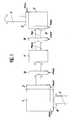
- FIG. 1 represents in its most general form a logic network of dynamic type according to the invention. Conventionally, it comprises a first matrix 1 receiving logic input variables E and a second matrix 2 delivering one or more signals S representing one or more logic functions of input variables E.
- the two matrices 1, 2 are constituted by a plurality of logic gates, these logic gates being able to be AND, OR, NOR, NON-AND gates.
- the type of logic gates used in each of the matrices can obviously be chosen taking into account the logic functions that one wishes to achieve.
- these logic gates are of dynamic type and must work in two phases: a first phase of precharging their output lines, defined respectively by the signals PH1 and PH0 for the first and the second matrix and a second phase functional defined respectively by PH0 and PH1 for the first and the second matrix.
- the precharge means of the first matrix are constituted by precharge circuits 3 putting the output lines ME of this matrix into communication with a supply voltage source. Furthermore, the precharging means comprise a circuit 4 for forcing the input lines of the first matrix to a determined voltage. These input forcing voltages will obviously be chosen as a function of the output precharging voltage and of the type of logic gate used in the first matrix. For example, if NI gates made using NMOS transistors are used, the output line of these gates is preloaded at a positive voltage, for example 5 volts and it will then be necessary for all the input lines of the matrix are forced to the value 0 volt. These two circuits 3, 4 of the precharge means are made active by the phase signal PH1 or a signal which is a function of the latter.
- NAND gates made using PMOS transistors having their source connected to a positive voltage are used, the drains being interconnected to constitute the output of the door, the output will be preloaded at 0 volts and the inputs will be forced to a positive voltage.
- the second matrix 2 is associated with precharge means 5,6, these precharge means being constituted by a precharge circuit 5 of the output lines of this matrix and circuit 6 allowing the input lines to be forced to a suitable voltage.
- precharge means 5,6 are activated by the signal PH0 or a function signal from PH0.
- the output lines ME of the first matrix are connected to storage means 7 by means of isolation means 8 controlled by the signal PH0.
- the isolation means 8 function as switches which close in the presence of the signal PH0.
- a switch is interposed between each output line of the first matrix and the corresponding input line of the storage means 7.
- These storage means 7 are constituted by as many storage cells as the matrix 1 has outputs.
- the output lines MEO of the storage means 7 are connected to the second isolation means 9. These second isolation means have a function similar to that of the first isolation means 8. They are controlled by the signal PH1, and are close when this signal is present.
- the output lines MO of the second isolation means 9 are connected to the input lines of the second matrix 2 via the forcing circuit 6.
- the output lines S of the second matrix 2 are precharged to a determined voltage by means of the precharging circuit 5.
- the input lines of the second matrix 2 receive a forcing voltage by circuit 6.
- the means 9 isolate the output of the storage means 7 of the circuit 6.
- the first isolation means 8 put in communication the output lines ME of the first matrix 1 with the inputs of the storage means 7 Finally, the precharge circuits 3 and 4 are inhibited.
- the precharging circuits 3,4 of the first matrix which are made active while the first isolation means 8 isolates the storage means 7 of the first matrix.
- the precharge circuits 5 and 6 of the second matrix 2 are inactive.
- the second isolation means 9 allow the transfer of the signals stored during the previous phase in the storage means 7 to the inputs of the second matrix 2.
- the first matrix 1 is well preloaded and can therefore start a new functional phase as described above.
- the logic network represented in FIG. 1 does indeed allow operation in two clock phases only. This is made possible by the presence of the storage means 7 and the first and second isolation means 8 and 9 which allow the functional phase of one of the matrices to coincide with the precharge phase of the other matrix and vice versa.
- the two matrices 1 and 2 are formed by networks of n-channel field effect transistors of the NMOS type connected so as to form NI logic gates. For reasons of clarity, only one logical gate has been shown per matrix.
- p-channel field effect transistors are represented with a small circle drawn on their grid.
- One of the logic gates NI of the first matrix is constituted by transistors TEi0 ... TEin having their source connected to ground and their drain connected to one of the output lines MEi of the first matrix.
- the gates of these transistors respectively receive the signals E0 ... From an associated circuit.
- P6 associated with the first transistor TEi0 is shown in FIG. 2.
- This circuit comprises a first field effect transistor with p channel P6 whose source is connected to a supply voltage positive Vdd and whose drain is connected to the drain of an n-channel field effect transistor N4 and to the gate of the transistor TE0.
- the source of transistor N4 is connected to ground.
- This last transistor N4 receives on its gate the signal PH1 defining the second clock phase.
- the gate of transistor P6 is connected to the output of a NAND gate 10 with two inputs, the first of its inputs receiving the signal PH0 defining the first clock phase, the second input receiving the logic variable e0. It should be noted that the signal e0 represents an input logic variable or its complement, depending on the logic function performed.
- the precharge circuit of the output line MEi is simply constituted by a p-channel field effect transistor P5 whose source is connected to a positive supply voltage Vdd and whose drain is connected to the line MEi.
- the complementary signal NPH1 of the signal PH1 is applied to the gate of the transistor P5.
- the n channel channel field effect transistors TOi ... TOj constitute a logic gate NI belonging to the second matrix 2.
- the source of each of these transistors is connected to ground and their drain is connected to one of the lines of output Sk of the second matrix 2.
- the gates of these transistors respectively receive the signals MOi ... MOj coming from an associated circuit. For reasons of clarity, only the circuit P1 to P4, N1 to N4 associated with the transistor TOi has been shown in FIG. 2.
- the precharge circuit of the output line Sk of the second matrix is produced by means of a p-channel field effect transistor P7 whose source is connected to a positive supply voltage Vdd and whose drain is connected to the output line S.
- the complementary signal NPH0 of the signal PH0 is applied to the gate of this transistor.
- the output line MEi of the first matrix is connected to the gate of an n-channel field effect transistor N2 and to the gate of a p-channel transistor P2 whose drains are connected together.
- the source of transistor P2 is connected to the drain of another p-channel transistor P1, the source of which is connected to a positive supply voltage Vdd.
- the gate of transistor P1 receives the complementary signal NPH0 from the signal PH0.
- the source of transistor N2 is connected to the drain of an n-channel transistor N1, the source of which is connected to ground.
- the gate of transistor N1 receives the signal PH0.
- the circuit formed by the transistors P1, P2, N2, N1 constitutes a three-state inverter.
- the MEO signal present on the drains of transistors N2 and P2 is applied to the gate of another p-channel transistor P4 whose source is connected to the drain of a p-channel transistor P3 having its source connected to a voltage of Vdd positive feed.
- the complementary signal NPH1 of the signal PH1 is applied to the gate of the transistor P3.
- the drain of transistor P4 is connected to the drain of another n-channel transistor N3, the source of which is connected to ground.
- the phase signal PH0 is applied to the gate of the transistor N3.
- the signal MOi present on the drains of transistors N3 and P4 is applied to the gate of the associated transistor TOi. According to the logic functions which it is desired to achieve by means of this logic network, the signal MOi can also be applied to the gate of another transistor forming part of another logic gate NI not shown in the second matrix.
- the precharge circuit 5 of the output lines of the second matrix 2 is constituted by as many transistors P7 as the second matrix has outputs.
- the precharge circuit 3 of the output lines of the first matrix 1 is constituted by as many transistors P5 as the first matrix has outputs.
- the forcing circuit 4 of the input lines of the first matrix is constituted by as many transistors N4 as the first matrix has inputs.
- the forcing circuit 6 of the input lines of the second matrix 2 is constituted by as many transistors N3 as this matrix has inputs.
- the first isolation means 8 consist of as many three-state inverters P1, P2, N2, N1 as the first matrix has output lines.
- the second isolation means 8 are constituted by the corresponding transistors P3.
- a storage cell associated with an output line of the first matrix is produced by the structure capacity of the transistor P4.
- the three-state inverter P1, P2, N2, N1 and the circuit formed by the transistors N3, P3, P4, also have an amplification function.
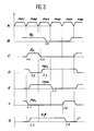
- the signals PH0 and PH1 of the timing diagram A define the two operating phases of the device. According to timing diagram A, the phases PH0 and PH1 were assumed to be adjacent but the same operation could be obtained by using two phase signals having a dead time between these two phases. The only condition is that the phases PH0 and PH1 do not overlap.
- the signal NPH0 complementary to the signal PH0 has the logic value 0 thus making the transistor P1 conductive.
- the signal PH0 applied to transistor N1 makes it driver.
- the three-state inverter P1, P2, N2, N1 operates as an inverter.
- the voltage MEO applied to the gate of the transistor P4 takes the logic value 1.
- the signal NPH1 applied to the gate of the transistor P3 is zero, which makes this transistor blocked.
- the signal PH0 applied to the gate of transistor N3 makes this latter conductor. It follows that, whatever the value of the voltage ME0, the voltage MOi applied to the transistor TOi becomes zero, thus bringing this transistor to the blocked state. Finally, the signal NPH0 having a zero voltage, the transistor T7 is made conductive. The output line Sk is thus preloaded at the voltage Vdd. This state appears from time t3 represented on the timing diagram G.
- the output voltage of gate 10 takes the logic value 1 as well as the voltage applied to the gate of transistor N4. This causes the signal E0 to go to 0, thus blocking the transistor TEi0. As the voltage applied to the gate of transistor P5 is zero, this transistor is conductive. As a result, the line MEi charges at the supply voltage Vdd, which is carried out at the instant t5 of the timing diagram D.
- the transistors P1 and N1 are blocked, which prevents any change in voltage of the MEO signal. This is the memorization effect sought.
- the transistor P3 is conductive and the transistor N3 is blocked. But as the gate voltage MEO of the transistor P4 has a positive value, this transistor remains blocked, maintaining at the value 0 the voltage of the signal MOi. As a result, the transistor TOi remains blocked and therefore does not modify the output voltage Sk, which retains the logic value 1 if none of the other transistors TOj have discharged the output line Sk.
- the transistors N3 and P7 become conductive from time t7 and the transistor P3 is blocked, thus allowing the precharge of the line Sk.
- the transistor P5 is blocked which authorizes a change of voltage of the line MEi.
- the transistor P6 is conductive, the transistor N4 being blocked. It follows that the voltage E0 keeps the value 0 thus maintaining the transistor TEi0 in the blocked state.
- the line MEi keeps a positive voltage, which maintains the voltage MEO of the gate of transistor P4.
- the transistors P1, N1, N3 are again blocked and the transistor P3 is conductive.
- the transistor P4 is made conductive which causes the signal MOi to go to the logic value 1 at time t8.
- the transistor TOi is made conductive, which produces the discharge at time t9 of the output line Sk.
Landscapes
- Physics & Mathematics (AREA)
- Mathematical Physics (AREA)
- Engineering & Computer Science (AREA)
- Computer Hardware Design (AREA)
- Computing Systems (AREA)
- General Engineering & Computer Science (AREA)
- Logic Circuits (AREA)
Applications Claiming Priority (2)
| Application Number | Priority Date | Filing Date | Title |
|---|---|---|---|
| FR8701741 | 1987-02-12 | ||
| FR8701741A FR2611099B1 (fr) | 1987-02-12 | 1987-02-12 | Reseau logique dynamique |
Publications (3)
| Publication Number | Publication Date |
|---|---|
| EP0282370A2 true EP0282370A2 (de) | 1988-09-14 |
| EP0282370A3 EP0282370A3 (en) | 1988-09-21 |
| EP0282370B1 EP0282370B1 (de) | 1991-07-24 |
Family
ID=9347832
Family Applications (1)
| Application Number | Title | Priority Date | Filing Date |
|---|---|---|---|
| EP88400303A Expired - Lifetime EP0282370B1 (de) | 1987-02-12 | 1988-02-10 | Dynamische logische Anordnung |
Country Status (6)
| Country | Link |
|---|---|
| US (1) | US4812685A (de) |
| EP (1) | EP0282370B1 (de) |
| JP (1) | JPH01218212A (de) |
| CA (1) | CA1284359C (de) |
| DE (1) | DE3863797D1 (de) |
| FR (1) | FR2611099B1 (de) |
Cited By (1)
| Publication number | Priority date | Publication date | Assignee | Title |
|---|---|---|---|---|
| EP0391379A2 (de) * | 1989-04-06 | 1990-10-10 | Oki Electric Industry Co., Ltd. | Schaltung einer programmierbaren logischen Anordnung |
Families Citing this family (5)
| Publication number | Priority date | Publication date | Assignee | Title |
|---|---|---|---|---|
| JP2547436B2 (ja) * | 1988-04-11 | 1996-10-23 | 富士通株式会社 | Pla制御方式 |
| US4912342A (en) * | 1988-05-05 | 1990-03-27 | Altera Corporation | Programmable logic device with array blocks with programmable clocking |
| US5070262A (en) * | 1988-10-06 | 1991-12-03 | Texas Instruments Incorporated | Signal transmission circuit |
| US5926038A (en) * | 1997-11-10 | 1999-07-20 | The United States Of America As Represented By The Secretary Of The Navy | Two-phase dynamic logic circuits for gallium arsenide complementary HIGFET fabrication |
| US7116131B1 (en) | 2004-09-15 | 2006-10-03 | Xilinx, Inc. | High performance programmable logic devices utilizing dynamic circuitry |
Citations (3)
| Publication number | Priority date | Publication date | Assignee | Title |
|---|---|---|---|---|
| US4381460A (en) * | 1980-05-27 | 1983-04-26 | National Semiconductor Corporation | Bootstrap driver circuit |
| JPS61101124A (ja) * | 1984-10-24 | 1986-05-20 | Hitachi Micro Comput Eng Ltd | 半導体集積回路装置 |
| DE3635761A1 (de) * | 1985-10-21 | 1987-04-23 | Western Digital Corp | Programmierbares logikfeld mit dynamischer cmos-logik |
Family Cites Families (8)
| Publication number | Priority date | Publication date | Assignee | Title |
|---|---|---|---|---|
| US4661922A (en) * | 1982-12-08 | 1987-04-28 | American Telephone And Telegraph Company | Programmed logic array with two-level control timing |
| JPS59125125A (ja) * | 1982-12-30 | 1984-07-19 | Fujitsu Ltd | プログラマブル・ロジツク・アレイ |
| US4577190A (en) * | 1983-04-11 | 1986-03-18 | At&T Bell Laboratories | Programmed logic array with auxiliary pull-up means to increase precharging speed |
| US4611133A (en) * | 1983-05-12 | 1986-09-09 | Codex Corporation | High speed fully precharged programmable logic array |
| JPS6169215A (ja) * | 1984-09-12 | 1986-04-09 | Nec Corp | プログラマブル・ロジツク・アレイ |
| IT1195119B (it) * | 1986-08-04 | 1988-10-12 | Cselt Centro Studi Lab Telecom | Perfezionamenti alle schiere logi che programmabili dinamiche a struttura nor nor realizzate in tecnolo gia c mos |
| US4760290A (en) * | 1987-05-21 | 1988-07-26 | Vlsi Technology, Inc. | Synchronous logic array circuit with dummy signal lines for controlling "AND" array output |
| JPH11651A (ja) * | 1997-06-12 | 1999-01-06 | Hitachi Ltd | 懸濁物除去装置 |
-
1987
- 1987-02-12 FR FR8701741A patent/FR2611099B1/fr not_active Expired - Fee Related
-
1988
- 1988-02-10 DE DE8888400303T patent/DE3863797D1/de not_active Expired - Lifetime
- 1988-02-10 EP EP88400303A patent/EP0282370B1/de not_active Expired - Lifetime
- 1988-02-10 US US07/154,340 patent/US4812685A/en not_active Expired - Fee Related
- 1988-02-11 CA CA000558713A patent/CA1284359C/fr not_active Expired - Lifetime
- 1988-02-12 JP JP63030670A patent/JPH01218212A/ja active Pending
Patent Citations (3)
| Publication number | Priority date | Publication date | Assignee | Title |
|---|---|---|---|---|
| US4381460A (en) * | 1980-05-27 | 1983-04-26 | National Semiconductor Corporation | Bootstrap driver circuit |
| JPS61101124A (ja) * | 1984-10-24 | 1986-05-20 | Hitachi Micro Comput Eng Ltd | 半導体集積回路装置 |
| DE3635761A1 (de) * | 1985-10-21 | 1987-04-23 | Western Digital Corp | Programmierbares logikfeld mit dynamischer cmos-logik |
Non-Patent Citations (3)
| Title |
|---|
| IBM TECHNICAL DISCLOSURE BULLETIN, vol. 24, no. 2, juillet 1981, pages 1165-1166, New York, US; W.R. KRAFT et al.: "Programmed logic array" * |
| IEEE JOURNAL OF SOLID-STATE CIRCUITS, vol. SC-11, no. 3, juin 1976, pages 370-374, New York, US; E. HEBENSTREIT et al.: "High-speed programmable logic arrays in ESFI SOS technology" * |
| PATENT ABSTRACTS OF JAPAN, vol. 10, no. 283 (E-440)[2339], 26 septembre 1986; & JP-A-61 101 124 (HITACHI MICRO COMPUT ENG. LTD) 20-05-1986 * |
Cited By (2)
| Publication number | Priority date | Publication date | Assignee | Title |
|---|---|---|---|---|
| EP0391379A2 (de) * | 1989-04-06 | 1990-10-10 | Oki Electric Industry Co., Ltd. | Schaltung einer programmierbaren logischen Anordnung |
| EP0391379A3 (de) * | 1989-04-06 | 1992-05-13 | Oki Electric Industry Co., Ltd. | Schaltung einer programmierbaren logischen Anordnung |
Also Published As
| Publication number | Publication date |
|---|---|
| FR2611099B1 (fr) | 1993-02-12 |
| US4812685A (en) | 1989-03-14 |
| EP0282370B1 (de) | 1991-07-24 |
| CA1284359C (fr) | 1991-05-21 |
| DE3863797D1 (de) | 1991-08-29 |
| FR2611099A1 (fr) | 1988-08-19 |
| JPH01218212A (ja) | 1989-08-31 |
| EP0282370A3 (en) | 1988-09-21 |
Similar Documents
| Publication | Publication Date | Title |
|---|---|---|
| EP0080394B1 (de) | Bistabile Kippschaltung mit energieunabhängiger Haltbarkeit und statischer Rücksetzung | |
| EP1863179B1 (de) | Niveauverschiebungsschaltkreis | |
| FR2488006A1 (fr) | Circuit de report perfectionne pour un additionneur binaire | |
| FR2593652A1 (fr) | Reseau logique programmable a logique dynamique a horloge unique. | |
| FR2544143A1 (fr) | Reseau logique programme comportant des moyens auxiliaires de connexion au potentiel positif pour augmenter la vitesse de precharge | |
| EP0591022A1 (de) | Spannungserhöhungsschaltung des Ladungspumpen-Typs mit Bootstrap-Oszillator | |
| FR2464535A1 (fr) | Systeme de memoire statique remanente a acces direct | |
| EP0262013B1 (de) | Leseverstärker | |
| FR2473814A1 (fr) | Circuit mos dynamique ne dependant pas d'un rapport de resistances destine a constituer des circuits logiques divers | |
| FR2687488A1 (fr) | Dispositif pour memoire a semi-conducteurs avec un circuit de generation d'un signal d'horloge pour des lignes de bit separees. | |
| FR2605768A1 (fr) | Dispositif de commande de bus constitue par plusieurs segments isolables | |
| EP0282370B1 (de) | Dynamische logische Anordnung | |
| FR2680025A1 (fr) | Circuit de transmission de donnees comportant une ligne d'entree/sortie commune. | |
| EP0194195B1 (de) | Statische bistabile Kippschaltung in CMOS-Technologie | |
| FR2641391A1 (fr) | Composant logique programmable effacable rapide | |
| FR2729782A1 (fr) | Cellule de memoire a cinq transistors comportant une ligne d'alimentation en energie partagee | |
| EP0905907B1 (de) | Exklusiv-Oder-Gatter mit vier zwei-zu-zwei komplementären Eingängen und zwei komplementären Ausgängen sowie Frequenzmultiplizierer damit | |
| EP0229433B1 (de) | Vorrichtung zum Prüfen eines kombinatorischen logischen Schaltkreises | |
| EP0283393A1 (de) | Binäre Rechnungseinrichtung | |
| EP0678868A1 (de) | Spannungsvervielfacherschaltung | |
| EP0140413B1 (de) | Dekodierschaltung für statischen RAM-Speicher | |
| EP0186533B1 (de) | Dynamisches Speicherelement und seine Verwendung in einer Master-Slave-Kippschaltung und in programmierbaren sequentiellen Schaltungen | |
| FR2676854A1 (fr) | Procede pour precharger des lignes d'entree/sortie d'un dispositif de memoire. | |
| FR2787212A1 (fr) | Circuit pour remettre a l'etat initial une paire de bus de donnees d'un dispositif de memoire a semiconducteur | |
| EP0750311B1 (de) | Leitungsverstärker für statische RAM-Speicher |
Legal Events
| Date | Code | Title | Description |
|---|---|---|---|
| PUAI | Public reference made under article 153(3) epc to a published international application that has entered the european phase |
Free format text: ORIGINAL CODE: 0009012 |
|
| PUAL | Search report despatched |
Free format text: ORIGINAL CODE: 0009013 |
|
| AK | Designated contracting states |
Kind code of ref document: A2 Designated state(s): BE CH DE FR GB IT LI LU NL SE |
|
| AK | Designated contracting states |
Kind code of ref document: A3 Designated state(s): BE CH DE FR GB IT LI LU NL SE |
|
| 17P | Request for examination filed |
Effective date: 19881006 |
|
| 17Q | First examination report despatched |
Effective date: 19900321 |
|
| GRAA | (expected) grant |
Free format text: ORIGINAL CODE: 0009210 |
|
| AK | Designated contracting states |
Kind code of ref document: B1 Designated state(s): BE CH DE FR GB IT LI LU NL SE |
|
| GBT | Gb: translation of ep patent filed (gb section 77(6)(a)/1977) | ||
| ITF | It: translation for a ep patent filed | ||
| REF | Corresponds to: |
Ref document number: 3863797 Country of ref document: DE Date of ref document: 19910829 |
|
| PLBE | No opposition filed within time limit |
Free format text: ORIGINAL CODE: 0009261 |
|
| STAA | Information on the status of an ep patent application or granted ep patent |
Free format text: STATUS: NO OPPOSITION FILED WITHIN TIME LIMIT |
|
| 26N | No opposition filed | ||
| EPTA | Lu: last paid annual fee | ||
| EAL | Se: european patent in force in sweden |
Ref document number: 88400303.9 |
|
| PGFP | Annual fee paid to national office [announced via postgrant information from national office to epo] |
Ref country code: SE Payment date: 19990125 Year of fee payment: 12 |
|
| PGFP | Annual fee paid to national office [announced via postgrant information from national office to epo] |
Ref country code: FR Payment date: 19990129 Year of fee payment: 12 |
|
| PGFP | Annual fee paid to national office [announced via postgrant information from national office to epo] |
Ref country code: BE Payment date: 19990208 Year of fee payment: 12 |
|
| PGFP | Annual fee paid to national office [announced via postgrant information from national office to epo] |
Ref country code: LU Payment date: 19990209 Year of fee payment: 12 |
|
| PGFP | Annual fee paid to national office [announced via postgrant information from national office to epo] |
Ref country code: GB Payment date: 19990211 Year of fee payment: 12 Ref country code: CH Payment date: 19990211 Year of fee payment: 12 |
|
| PGFP | Annual fee paid to national office [announced via postgrant information from national office to epo] |
Ref country code: NL Payment date: 19990228 Year of fee payment: 12 |
|
| PGFP | Annual fee paid to national office [announced via postgrant information from national office to epo] |
Ref country code: DE Payment date: 19990428 Year of fee payment: 12 |
|
| PG25 | Lapsed in a contracting state [announced via postgrant information from national office to epo] |
Ref country code: LU Free format text: LAPSE BECAUSE OF NON-PAYMENT OF DUE FEES Effective date: 20000210 Ref country code: GB Free format text: LAPSE BECAUSE OF NON-PAYMENT OF DUE FEES Effective date: 20000210 |
|
| PG25 | Lapsed in a contracting state [announced via postgrant information from national office to epo] |
Ref country code: SE Free format text: LAPSE BECAUSE OF NON-PAYMENT OF DUE FEES Effective date: 20000211 |
|
| PG25 | Lapsed in a contracting state [announced via postgrant information from national office to epo] |
Ref country code: BE Free format text: LAPSE BECAUSE OF NON-PAYMENT OF DUE FEES Effective date: 20000228 |
|
| PG25 | Lapsed in a contracting state [announced via postgrant information from national office to epo] |
Ref country code: LI Free format text: LAPSE BECAUSE OF NON-PAYMENT OF DUE FEES Effective date: 20000229 Ref country code: CH Free format text: LAPSE BECAUSE OF NON-PAYMENT OF DUE FEES Effective date: 20000229 |
|
| BERE | Be: lapsed |
Owner name: S.A. BULL Effective date: 20000228 |
|
| PG25 | Lapsed in a contracting state [announced via postgrant information from national office to epo] |
Ref country code: NL Free format text: LAPSE BECAUSE OF NON-PAYMENT OF DUE FEES Effective date: 20000901 |
|
| GBPC | Gb: european patent ceased through non-payment of renewal fee |
Effective date: 20000210 |
|
| EUG | Se: european patent has lapsed |
Ref document number: 88400303.9 |
|
| REG | Reference to a national code |
Ref country code: CH Ref legal event code: PL |
|
| PG25 | Lapsed in a contracting state [announced via postgrant information from national office to epo] |
Ref country code: FR Free format text: LAPSE BECAUSE OF NON-PAYMENT OF DUE FEES Effective date: 20001031 |
|
| NLV4 | Nl: lapsed or anulled due to non-payment of the annual fee |
Effective date: 20000901 |
|
| PG25 | Lapsed in a contracting state [announced via postgrant information from national office to epo] |
Ref country code: DE Free format text: LAPSE BECAUSE OF NON-PAYMENT OF DUE FEES Effective date: 20001201 |
|
| REG | Reference to a national code |
Ref country code: FR Ref legal event code: ST |
|
| PG25 | Lapsed in a contracting state [announced via postgrant information from national office to epo] |
Ref country code: IT Free format text: LAPSE BECAUSE OF NON-PAYMENT OF DUE FEES;WARNING: LAPSES OF ITALIAN PATENTS WITH EFFECTIVE DATE BEFORE 2007 MAY HAVE OCCURRED AT ANY TIME BEFORE 2007. THE CORRECT EFFECTIVE DATE MAY BE DIFFERENT FROM THE ONE RECORDED. Effective date: 20050210 |