EP0282279B1 - Vorrichtung zur Kompression und/oder Dehnung einer Zeitbasis - Google Patents
Vorrichtung zur Kompression und/oder Dehnung einer Zeitbasis Download PDFInfo
- Publication number
- EP0282279B1 EP0282279B1 EP88302040A EP88302040A EP0282279B1 EP 0282279 B1 EP0282279 B1 EP 0282279B1 EP 88302040 A EP88302040 A EP 88302040A EP 88302040 A EP88302040 A EP 88302040A EP 0282279 B1 EP0282279 B1 EP 0282279B1
- Authority
- EP
- European Patent Office
- Prior art keywords
- signal
- ccd
- clock
- pulse
- time base
- Prior art date
- Legal status (The legal status is an assumption and is not a legal conclusion. Google has not performed a legal analysis and makes no representation as to the accuracy of the status listed.)
- Expired - Lifetime
Links
Images


Classifications
-
- H—ELECTRICITY
- H04—ELECTRIC COMMUNICATION TECHNIQUE
- H04N—PICTORIAL COMMUNICATION, e.g. TELEVISION
- H04N5/00—Details of television systems
- H04N5/76—Television signal recording
- H04N5/91—Television signal processing therefor
- H04N5/92—Transformation of the television signal for recording, e.g. modulation, frequency changing; Inverse transformation for playback
-
- G—PHYSICS
- G11—INFORMATION STORAGE
- G11C—STATIC STORES
- G11C19/00—Digital stores in which the information is moved stepwise, e.g. shift registers
- G11C19/28—Digital stores in which the information is moved stepwise, e.g. shift registers using semiconductor elements
- G11C19/282—Digital stores in which the information is moved stepwise, e.g. shift registers using semiconductor elements with charge storage in a depletion layer, i.e. charge coupled devices [CCD]
- G11C19/285—Peripheral circuits, e.g. for writing into the first stage; for reading-out of the last stage
-
- G—PHYSICS
- G11—INFORMATION STORAGE
- G11C—STATIC STORES
- G11C27/00—Electric analogue stores, e.g. for storing instantaneous values
- G11C27/04—Shift registers
-
- H—ELECTRICITY
- H04—ELECTRIC COMMUNICATION TECHNIQUE
- H04N—PICTORIAL COMMUNICATION, e.g. TELEVISION
- H04N5/00—Details of television systems
- H04N5/14—Picture signal circuitry for video frequency region
-
- H—ELECTRICITY
- H04—ELECTRIC COMMUNICATION TECHNIQUE
- H04N—PICTORIAL COMMUNICATION, e.g. TELEVISION
- H04N9/00—Details of colour television systems
- H04N9/79—Processing of colour television signals in connection with recording
Definitions
- This invention generally relates to an apparatus for compressing and/or expanding the time base of a signal and, more particularly, is directed to such an apparatus using a charge coupled device (hereinafter CCD).
- CCD charge coupled device
- the CCD used in such an apparatus is a semiconductor chip on which is formed a charge transfer channel surrounded by channel stop regions; the charge transfer channel is provided with, for example, transfer electrodes of two-phase type disposed thereon, and the CCD is driven with a two-phase transfer clock pulse signal applied to the transfer electrodes.
- the desired length of the charge transfer channel is achieved by effectively utilising the space on the semiconductor chip. To do this, the charge transfer channel is arranged to have bend portions as shown in fig 1.
- the charge transfer channel 13 surrounded by channel stop regions 11 has a bend portion 13a and the direction of transfer of the electric charges is reversed at the bend portion 13a.
- the CCD When compression or expansion of the time base of a video signal is performed using such a CCD, the CCD is driven by a transfer clock pulse signal at a predetermined frequency for writing, whereby the video signal is written to the CCD. In succession thereto, the CCD is driven by a transfer clock pulse signal of a different frequency so as to read the video signal out of the CCD at a different rate.
- a video signal is supplied to the CCD, and at the same time, the transfer electrodes 15a and 15b disposed on the charge transfer channel 13 are supplied with pulse train signals P ⁇ 1 and P ⁇ 2, as the two-phase transfer clock pulse signal for writing, respectively, which have a duty cycle of 50% and a period of Tw and are 180° out of phase with each other as shown in fig 2.
- the CCD is driven and the signal charges based upon the video signal are transferred through the charge transfer channel 13 and, as a result, a predetermined portion of the video signal for, for example, one horizontal line, is written into the charge transfer channel 13.
- the transfer electrodes 15a and 15b disposed on the charge transfer channel 13 are supplied with pulse train signals Q ⁇ 1 and Q ⁇ 2, as the two-phase transfer clock pulse signal for reading, respectively, which have a duty cycle of 50% and a period of Tr corresponding, for example, to a half of the period Tw and are 180° out of phase with each other as shown in fig 2.
- the CCD is driven and the signal charges based upon the video signal written in the charge transfer channel 13 is transferred therethrough, and as a result, a video signal corresponding to one horizontal line is read out of the charge transfer channel 13.
- the video single written in the CCD with the two-phase transfer clock pulse signal for writing have a period Tw
- the video signal read out from the CCD has its time base compressed to a half of that of the original video signal.
- the charge transfer channel of the CCD used, for example, for compressing the time base of a video signal has bend portions as shown in fig 1, and it is considered that there are energy "defects" in such bend portions, and therefore, when charges are transferred therethrough, some charges remain untransferred in such a defect".
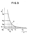
- the quantity of the remaining, or residual, charges in the "defect” varies according to the pulse width of the transfer clock pulse signal at the time of the charge transferring operation. For example, as shown by a curve X in fig 3 indicating the relationship between the quantity of the residual charge q in such a "defect" and the pulse width ⁇ of the transfer clock pulse signal, the smaller the pulse width ⁇ is, the large becomes the quantity of the residual charge q.
- Such residual charges produced in the bend portion of the charge transfer channel at the time of charge transfer operation through the charge transfer channel of the CCD does not cause any noise component in the output signal from the CCD as long as their quantity is kept constant, but if the quantity varies, that is, if the pulse width of the transfer clock pulse signal varies, it causes changes in the quantity of the transferred signal charges, and as a result, noise components are produced in the output signal from the CCD.
- the transfer clock pulse signal changes from the two-phase transfer clock pulse signal for writing to the two-phase transfer clock pulse signal for reading between the write mode period and the succeeding read mode period, and therefore, the period of the transfer clock pulse signal changes from Tw to Tr, which corresponds to a half of Tw, and the pulse width also changes from Tw/2 to Tr/2.
- the video signal output from the CCD tends to include a noise component at the portion corresponding to the signal charge transferred through the bend portion of the charge transfer channel at the beginning of the read mode period.
- the noises take on a fixed pattern and become very conspicuous.
- the present invention has as its object the provision of a time base compressing and/or expanding apparatus, which, using a CCD having its charge transfer channel provided with bend portions therein, functions to compress or expand the time base of an input signal supplied to the CCD and provide the same at the output side of the CCD, and further, is capable of effectively reducing the noise components liable to be included in the signal obtained from the output side of the CCD due to the charge transfer operation through the bend portions in the charge transfer channel of the CCD.
- apparatus for compressing and/or expanding the time base of an input signal characterised in that it comprises: charge coupled device means having an input terminal which in use is supplied with said input signal, an output terminal, first and second clock terminals, and a charge transfer channel through which charges corresponding to said input signal are transferred, said charge transfer channel having bend portions at which the direction of the charge transfer is changed, clock generating means for generating a write clock signal and a read clock signal in a time-divisional manner, the frequency of said read clock signal being different from that of said write clock signal, and clock driver means selectively supplied with one of said write and read clock signals for generating first and second pulse trains to be supplied to said first and second clock terminals, respectively, when said write clock signal is supplied and generating third and fourth pulse trains to be supplied to said first and second terminals, respectively, when said read clock signal is supplied, said first pulse train being 180° out of phase with said second pulse train and said third pulse train being 180° out of phase with said fourth pulse train the pulse width of said first pulse
- writing the input signal to the CCD is performed by transferring operations of signal charges through the charge transfer channel of the CCD according to the first two-phase transfer clock pulse signal made up of the first and second pulse train signals and, in succession thereto, reading out of the CCD the signal obtained from the input signal with its time base compressed or expanded is performed by transferring operations of signal charges through the charge transfer channel of the CCD according to the second two-phase transfer clock pulse signal made up of the third and fourth pulse train signals.
- Fig 4 shows an example of a time base compressing and/or expanding apparatus according to the present invention and this example is that adapted for compressing the time base of a video signal.
- an input video signal Vi from an input terminal 21 is supplied to the input terminal of a CCD 22.
- the CCD 22 is a semiconductor chip in which a charge transfer channel is formed surrounded by channel stop regions. So that the space on the semiconductor chip may be effectively utilised the charge transfer channel is arranged to have bend portions as indicated in the charge transfer channel 13 of fig 1.
- Such a CCD 22 is provided with two-phase type transfer electrodes disposed on the charge transfer channel and adapted to be driven by two-phase transfer clock pulses applied to the transfer electrodes. Driven by the two-phase transfer clock pulses, the CCD performs writing of the video signal Vi input from the input terminal 21 and reading of the written video signal Vi.
- a driver circuit portion 23 consisting of a pulse generator 24 and a clock driver 25 for forming two-phase transfer clock pulse signals to be supplied to CCD 22, the signals corresponding to each of the write mode in which the video signal Vi from the input terminal 21 is written to the CCD 22 and the read mode in which the written video signal Vi is read out from the CCD 22.
- the pulse generator 24 is supplied with a mode selector signal Ss from a terminal 26.
- the output terminal of the CCD 22 is connected through a low-pass filter (LPF) 27 to an output terminal 28.
- LPF low-pass filter
- the write mode is established, and in the write mode, the mode selector signal Ss from the terminal 26 is made to take the low level L as shown in fig 5A.
- the clock driver 25, responding to the pulse train signal P generates, as shown in figs 5C and 5D, a pulse train signal P ⁇ 1 formed of successive pulses having a period Tw and a pulse width ⁇ 3 smaller than ⁇ 1/2 and a pulse train signal P ⁇ 2 formed of successive pulses having a period Tw and a pulse width ⁇ 4 larger than ⁇ 1 and arranged to be 180° out of phase with the pulse train signal P ⁇ 1, and supplies these pulse train signals P ⁇ 1 and P ⁇ 2 to the CCD 22 as the two-phase transfer clock pulse signal for writing.
- the CCD 22 is driven by the pulse train signals P ⁇ 1 and P ⁇ 2, whereby the transfer of signal charges based upon the video signal Vi is performed through the charge transfer channel of the CCD 22 and the video signal Vi for a predetermined portion, for one horizontal period, for example, is written into the charge transfer channel of the CCD 22.
- the mode selector signal Ss from the terminal 26 is made to take the high level H as shown in fig 5A.
- the CCD 22 is driven by the pulse train signals Q ⁇ 1 and Q ⁇ 2, whereby the transfer of signal charges through the charge transfer channel of the CCD 22 based upon the video signal Vi written therein is performed and the video signal Vi for one horizontal period is read out.
- the video signal Vi written to the CCD 22 driven by the two-phase transfer clock pulse writing signal consisting of the pulse train signals P ⁇ 1 and P ⁇ 2 whose period is Tw and then having the signal read out from the CCD 22 driven by the two-phase transfer clock pulse reading signal consisting of the pulse train signals Q ⁇ 1 and Q ⁇ 2 whose period is Tr corresponding to Tw/2
- the video signal read out of the CCD 22 has its time base compressed to a half of that of the original video signal Vi.
- the video signal thus read out of the CCD 22 is delivered through the low-pass filter 27, wherein its clock pulse signal component is removed, to the output terminal 28, and thereby, a video signal Vo whose time base has been compressed can be obtained from the output terminal 28.
- the aforementioned pulse widths ⁇ 1 to ⁇ 5, obey the relationship ⁇ 3 ⁇ ⁇ 2 ⁇ ⁇ 5 ⁇ ⁇ 1 ⁇ ⁇ 4.
- Supposing tha transfers through the charge transfer channel of a CCD 22 are performed by the transfer clock pulse signals each thereof having the pulse width ⁇ 1 - ⁇ 5, the quantities of the residual charges at the energy "defect" at the bend portion of the charge transfer channel of the CCD 22 will become q1, q2, q3, q4 and q5 corresponding to the pulse widths ⁇ 1 - ⁇ 5, respectively, as indicated in fig 3 relative to the curve X, and it is thereby known that there is the relationship q3 > q2 > q5 > q1 > q4 among these charge quantities q1 - q5.
- the signal transfer through the charge transfer channel of the CCD 22 during the write mode period is performed by the pulse train signal formed of pulses having the pulse width ⁇ 3 as the clock pulse signal of one phase of the two-phase transfer clock pulse signal and by the pulse train signal P' ⁇ 2 formed of pulses having the pulse width ⁇ 4 as the clock pulse signal of the other phase of the two-phase transfer clock pulse signal, and that during the read mode period following the write mode period is performed by the pulse train signal Q ⁇ 1 formed of pulses having the pulse width ⁇ 3 as the clock pulse signal of one phase of the two-phase transfer clock pulse signal and by the pulse train signal Q ⁇ 2 formed of pulses having the pulse width ⁇ 5 as the clock pulse signal of the other phase of the two-phase transfer clock pulse signal.
- the period of the clock pulse signal of the one phase of the two-phase transfer clock pulse signal causing the signal charges to transfer through the transfer channel of the CCD 22 changes from Tw to Tr but the pulse width thereof is kept unchanged to be ⁇ 3, whereas the period of the clock pulse signal of the other phase of the two-phase transfer clock pulse signal changes from Tw to Tr and the pulse width thereof changes from ⁇ 4 to ⁇ 5.
- the residual charge quantity q3 corresponding to the pulse width ⁇ 3 and the residual charge quantity q4 corresponding to the pulse width ⁇ 4 are produced at the bend portion of the charge transfer channel of the CCD 22 in the write mode, and the residual charge quantity q3 corresponding to the pulse width ⁇ 3 and the residual charge quantity q5 corresponding to the pulse width ⁇ 5 are produced in the read mode, and therefore, the change from the residual charge quantity q4 to the residual charge quantity q5 only is produced as the change in the residual charge quantity at the bend portion of the charge transfer channel of the CCD 22 accompanying the switching from the write mode to the read mode.
- the change in the residual charge quantity at the bend portion of the charge transfer channel of the CCD 22 is not produced by the clock pulse signals of the one phase of the two-phase transfer clock pulse signals, but produced only by the clock pulse signals of the other phase of the two-phase transfer clock pulse signals as the change from the residual charge quantity q4 to the residual charge quantity q5 due to the change from the pulse width ⁇ 4 to the pulse width ⁇ 5.
- the pulse width ⁇ 3 is made smaller than a half of the pulse width ⁇ 1, and also, the pulse width ⁇ 5 is made larger than the pulse width ⁇ 2, and therefore, both the residual charge quantity q4 and the residual charge quantity q5 are made relatively small, and further, the difference between the residual charge quantity q4 and the residual charge quantity q5, (q5 - q4), is made relatively small.
- the change in the residual charge quantity from the residual charge quantity q4 to the residual charge quantity q5 is kept relatively small.
- the noise components included in the output signal Vo due to the change in the residual charge quantity at the bend portion of the charge transfer channel of the CCD 22 are effectively reduced.
- the pulse train signals P ⁇ 1 and Q ⁇ 1 as the clock pulse signals of the one phase of the two-phase transfer clock pulse signals during the write mode period and the succeeding read mode period are made of pulses having the common pulse width ⁇ 3, the level of the video signal Vo, of which the time base has been compressed, obtained from the output side of the CCD 22 and through the low-pass filter 27 at the output terminal 28 is kept at a stabilised level.
- the apparatus according to the present invention can also be used for expansion of the time base of the signal in the CCD 22 by making the period of the two-phase transfer clock pulse signal for reading to be supplied to the CCD 22 during the read mode larger than the period of the two-phase transfer clock pulse signal for writing to be supplied to the CCD 22 during the write mode.
- the pulse width and used as the clock pulse signals of the one phase of the two-phase transfer clock pulse signals during the write mode period and the read mode period in succession thereto are selected to be such that the common pulse width is smaller than the pulse width of the pulse train signal supplied from the pulse generator 24 during the write mode period.
- the transfer pulse width ⁇ 3 of the transfer clock pulse signal corresponds to a very short period of time (for example, tens of a nano-second), and therefore, in order to generate such a transfer clock pulse signal of a constant pulse width, it becomes necessary to use, for example, a high speed device such as ECL as the monostable multivibrator for generating the pulse signal.
- a high speed device such as ECL
- the power consumption becomes large and the circuit itself might become large and expensive. Therefore, an example of a clock driver free from such disadvantages is shown in fig 6.
- 31 denotes a D flip-flop formed, for example, of high speed C-MOS gates.
- the input terminal D of the D flip-flop 31 is connected to a power supply terminal +B, the inverting output terminal Q of the D flip-flop 31 is grounded through a series circuit of a resistor 32 and a capacitor 33, the junction point K of the resistor 32 and the capacitor 33 is connected with the reset terminal R of the D flip-flop 31, and the resistor 32 is shunted by a diode 34.
- the input terminal 35 to be supplied with input pulse signals, ie, the pulse train signals P, Q in the present example, is connected with the clock terminal C of the D flip-flop 31 and the output terminals 36 and 37 are lead out from the non-inverting output terminal Q and the inverting output terminal Q of the same.
- the signal obtained at the inverting output terminal Q of the D flip-flop 31 goes from high level "1" to low level "0".
- the charge stored on the capacitor 33 during the period at high level "1” is gradually discharged through the resistor 32 until, after a predetermined period of time, the voltage at the junction point K drops to the reset voltage whereby the D flip-flop 31 is reset.
- the predetermined period of time can be adjusted by changing the values of the resistor 32 and the capacitor 33, and it is set, as described below, to ⁇ 3 in the present example.
- 101 and 103 denote CCDs each thereof having a number of bits (stages) for one horizontal period (n bits).
- 102 and 104 denote CCDs each thereof having a number of bits for two horizontal periods (2n bits).
- the CCDs 101, 103 are supplied with the red colour-difference signal R-Y (as shown in fig 9A) from a terminal 105, and the CCDs 102, 104 are supplied with the blue-colour difference signal B-Y (as shown in fig 9B) from another terminal 106.
- Output signals of the CCDs 101-104 are respectively, supplied to terminals a-d of a switch circuit 107 and the output signal of the switch circuit 107 is applied to an output terminal 109 via a low-pass filter 108.
- a clock signal as shown in fig 9D is supplied from a terminal 110 to the CCDs 101, 102. That is, one clock pulse at frequency f c is supplied during the first horizontal period H1 and two clock pulses at frequency 2f c are supplied during the second horizontal period H2.
- a clock signal as shown in fig 9E is supplied from a terminal 111 to the CCDs 103, 104. That is, two clock pulses at frequency 2f c are supplied during the first horizontal period H1 and one clock pulse at frequency f c is supplied during the second horizontal period H2.
- the switch circuit 107 is supplied with a control signal S sw1 from a terminal 112 and this switch circuit 107 is switched so as to be connected to the sides of c, d, a and b, during the first half and second half of the first horizontal period H1 and the first half and the second half of the second horizontal period H2, respectively.
- the colour-difference signals R-Y and B-Y for one horizontal period are written into the CCD 101 and the first half of the CCD 102 respectively.
- the colour-difference signal R-Y for one horizontal period is read out from the CCD 101, while the colour-difference signal B-Y which has been written in the first half of the CCD 102 is transferred to the second half.
- the colour-difference signal R-Y read out from the CCD 101 is delivered through the switch circuit 107 and the low-pass filter 108 to the output terminal 109.
- the colour-difference signal B-Y for one horizontal period is read out from the CCD 102.
- This colour-difference signal B-Y is delivered through the switch circuit 107 and the low-pass filter 108 to the output terminal 109.
- the colour-difference signals R-Y and B-Y for one horizontal period are written into the CCD 103 and the first half of the CCD 104, respectively. Further, according to the clock pulse at the frequency 2f c during the first half of the succeeding first horizontal period H1, the colour-difference signal R-Y for one horizontal period is read out from the CCD 103, while the colour-difference signal B-Y which has been written in the first half of the CCD 104 is transferred to the second half.
- the colour-difference signal R-Y read out from the CCD 103 is delivered through the switch circuit 107 and the low-pass filter 108 to the output terminal 109.
- the colour-difference signal B-Y for one horizontal period is read out from the CCD 104.
- This colour-difference signal B-Y is delivered through the switch circuit 107 and the low-pass filter 108 to the output terminal 109.
- a signal S c in which the colour-difference signals R-Y, B-Y each are compressed to a half along the time base and thereby time-division multiplexed as shown in fig 9C is obtained from the output terminal 109.
- the clock pulses are continuously supplied to the CCDs 101-104, and therefore, lattice defect noise due to the partially broken clock pulses can be prevented from occurring.
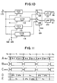
- Fig 10 shows an example of a time base expanding circuit for obtaining original colour-difference signals R-Y, B-Y from the time-divisionally multiplexed signal S c .
- 111 and 113 denote CCDs each thereof having a number of bits for one horizontal period (n bits).
- 112 and 114 denote CCDs each thereof having the number of bits for two horizontal periods (2n bits).
- the CCDs 111-114 are supplied with the time-division multiplexed signal S c (as shown in fig 11A) from a terminal 115.
- Output signals of the CCDs 111 and 113 are supplied to terminals a and b of a switch circuit 116, respectively, and the output signal of the switch circuit 116 is led out to an output terminal 118 through a low-pass filter 117.
- Output signals of the CCDs 112 and 114 are supplied to terminals a and b of a switch circuit 119, respectively, and the output signal of the switch circuit 119 is led out to an output terminal 121 through a low-pass filter 120.
- a clock signal as shown in fig 11D is supplied from a terminal 122 to the CCDs 111, 112. That is, two clock pulses at frequency 2f c are supplied during the first horizontal period H1 and one clock pulse at frequency f c is supplied during the second horizontal period H2.
- a clock signal as shown in fig 11E is supplied from a terminal 123 to the CCDs 113, 114. That is, one clock pulse at frequency f c is supplied during the first horizontal period H1 and two clock pulses at frequency 2f c are supplied during the second horizontal period H2.
- the switch circuits 116, 119 are supplied with a control signal S sw2 from a terminal 124 and these switch circuits 116, 119 are switched so as to be connected to the sides of b and a during the first horizontal period Hw and the second horizontal period H2 respectively.
- the colour-difference signal R-Y for one horizontal period is written into each of the CCD 111 and the fist half of the CCD 112.
- the colour-difference signal B-Y for one horizontal period is written into each of the CCD 111 and the first half of the CCD 112, while the colour-difference signal R-Y for one horizontal period which has been written in the first half of the CCD 112 is transferred to the second half.
- the colour-difference signals B-Y and R-Y each for one horizontal period are read out from the CCDs 111 and 112 and delivered through the switch circuits 116 and 119 and the low-pass filters 117 and 120 to the output terminals 118 and 121 respectively.
- the colour-difference signal R-Y for one horizontal period is written into each of the CCD 113 and the first half of the CCD 114.
- the colour-difference signal B-Y for one horizontal period is written into each of the CCD 113 and the first half of the CCD 114, while the colour-difference signal R-Y for one horizontal period which has been written in the first half of the CCD 114 is transferred to the second half.
- the colour-difference signals B-Y and R-Y each for one horizontal period are read out from the CCDs 113 and 114 and delivered through the switch circuits 116 and 119 and the low-pass filters 117 and 120 to the output terminals 118 and 121, respectively.
- the blue colour-difference signal B-Y and the red colour-difference signal R-Y are continuously obtained at the output terminals 118 and 121.
- the clock pulses are continuously supplied to the CCDs 111-114 also in the time base expanding circuit in the example of fig 10, and, therefore, lattice defect noise can be prevented from occurring.
- a CCD therein having a charge transfer channel disposed thereon with bend portions therein is supplied with an input signal and the writing of the input signal to the CCD and the reading of the written signal from the CCD are carried out according to improved transfer clock pulse signals, whereby the input signal supplied to the CCD can be output from the output side of the CCD with its time base compressed or expanded, and further, the noise component which may be caused by the signal charge transfer operation through the bend portion in the charge transfer channel of the CCD and included in the output signal delivered to the output side of the CCD with its time base compressed or expanded can be effectively decreased.
Landscapes
- Engineering & Computer Science (AREA)
- Multimedia (AREA)
- Signal Processing (AREA)
- Transforming Light Signals Into Electric Signals (AREA)
- Television Signal Processing For Recording (AREA)
- Lubrication Of Internal Combustion Engines (AREA)
- Shaping By String And By Release Of Stress In Plastics And The Like (AREA)
- Yarns And Mechanical Finishing Of Yarns Or Ropes (AREA)
- Filters That Use Time-Delay Elements (AREA)
- Compression Or Coding Systems Of Tv Signals (AREA)
- Absorbent Articles And Supports Therefor (AREA)
- Superconductors And Manufacturing Methods Therefor (AREA)
- Investigation Of Foundation Soil And Reinforcement Of Foundation Soil By Compacting Or Drainage (AREA)
Claims (7)
- Vorrichtung zur Kompression und/oder Dehnung einer Zeitbasis eines Eingangssignals,
gekennzeichnet durch
einer ladungsgekoppelten Einrichtung (22) mit einem zum Zuführen des Eingangssignals verwendeten Eingangsanschluß (21), einem ersten und zweiten Taktanschluß und einem Ladungsübertragungskanal (13), durch welchen mit dem Eingangssignal korrespondierende Ladungen übertragen werden, wobei der Ladungsübertragungskanal (13) gebogene Bereiche (13A) aufweist, bei welchen die Richtung der Ladungsübertragung geändert wird,
einer Takterzeugungseinrichtung (24) zu einer zeitaufgeteilten Erzeugung eines Schreibtaktsignals (P) und eines Lesetaktsignals (Q), wobei die Frequenz des Lesetaktsignals (Q) von der Frequenz des Schreibtaktsignals (P) verschieden ist, und eine selektiv mit dem Schreibtaktsignal (P) und Lesetaktsignal (Q) bedienten Taktbetriebseinrichtung (25) zur Erzeugung eines dem ersten und zweiten Taktanschluß zuzuführenden ersten bzw. zweiten Impulszuges (P'φ1, P'φ2) beim Zuführen des Schreibtaktsignals (P) und Erzeugen eines dem ersten und zweiten Anschluß zuzuführenden dritten bzw. vierten Impulszuges (Q'φ1, Q'φ2) beim Zuführen des Lesetaktsignals (Q), wobei der erste Impulszug (P'φ1) gegenüber dem zweiten Impulszug (P'φ2) um 180° phasenverschoben ist, und der dritte Impulszug (Q'φ1) gegenüber dem vierten Impulszug (Q'φ2) um 180° phasenverschoben ist, und wobei die Impulsbreite des ersten Impulszuges (P'φ1) im wesentlichen gleich der Impulsbreite des dritten Impulszuges (Q'φ1) und kleiner als die Hälfte der kürzeren von zwei Taktperioden, einer Schreibtaktperiode (Tw) und einer Lesetaktperiode (Tr), ist. - Vorrichtung nach Anspruch 1,
dadurch gekennzeichnet, daß
das Taktverhältnis des Schreibtaktsignals (P) und des Lesetaktsignals (Q) 50% beträgt. - Vorrichtung nach Anspruch 1 oder 2,
dadurch gekennzeichnet, daß
die Taktbetriebseinrichtung (25) ein D-Flip-Flop (31) mit einem an eine erste Bezugsspannungquelle (+B) angeschlossenen Dateneingangsanschluß (D), einem ersten und zweiten Ausgangsanschluß (Q,Q ), deren einer durch eine Serienschaltung aus einem durch eine Diode (34) nebengeschlossenen Widerstand (32) und einem Kondensator (33) an eine zweite Bezugsspannungsquelle angeschlossen ist, einem an die Verbindung des Widerstandes (32) und des Kondensators (33) angeschlossenen Rücksetzanschluß (R) und einem Taktanschluß (31), dem bei Benutzung das Ausgangssignal der Takterzeugungseinrichtung (24) zugeleitet ist. - Vorrichtung nach einem der vorhergehenden Ansprüche,
dadurch gekennzeichnet, daß
die Frequenz des Schreibtaktsignals (P) niedriger als die Frequenz des Lesetaktsignals (Q) ist, wodurch die Zeitbasis des Eingangssignals komprimiert wird. - Vorrichtung nach Anspruch 1, 2 oder 3,
dadurch gekennzeichnet, daß
die Frequenz des Schreibtaktsignals (P) höher als die Frequenz des Lesetaktsignals (Q) ist, wodurch die Zeitbasis des Eingangssignals gedehnt wird. - Vorrichtung nach einem der vorhergehenden Ansprüche,
dadurch gekennzeichnet, daß
die Zeitbasis ein Paar Chrominanz- oder Farbdifferenzsignale eines Videosignals aufweist, wobei für jedes dieser Signale je ein Paar ladungsgekoppelter Vorrichtungen (102, 104; 101, 103) vorgesehen ist, wobei das einem dieser Signale zugordnete Paar ladungsgekoppelter Einrichtungen (102, 104) eine Speicherkapazität für ein Zeitsegment des Videosignals aufweisen, die zwei Mal so groß ist, wie jene des anderen Paares ladungsgekoppelter Einrichtungen (101, 103), wobei die jeweiligen Signale den zugeordneten Paaren ladungsgekoppelter Einrichtungen zugeleitet sind und die Ausgangssignale der jeweiligen ladungsgekoppelten Einrichtungen derart abgetastet sind, daß ein die Chrominanz- oder Farbdifferenzsignale enthaltendes einzelnes Ausgangssignal zeitverschachtelt erhalten ist. - Vorrichtung nach Anspruch 6,
gekennzeichnet durch
durch eine ladungsgekoppelte Einrichtung zur Entschachtelung und Zeitbasisdehnung der in den Ausgangssignalen enthaltenen Signale.
Priority Applications (1)
| Application Number | Priority Date | Filing Date | Title |
|---|---|---|---|
| AT88302040T ATE97533T1 (de) | 1987-03-12 | 1988-03-09 | Vorrichtung zur kompression und/oder dehnung einer zeitbasis. |
Applications Claiming Priority (2)
| Application Number | Priority Date | Filing Date | Title |
|---|---|---|---|
| JP57818/87 | 1987-03-12 | ||
| JP62057818A JPS63224488A (ja) | 1987-03-12 | 1987-03-12 | 時間軸圧縮伸長装置 |
Publications (3)
| Publication Number | Publication Date |
|---|---|
| EP0282279A2 EP0282279A2 (de) | 1988-09-14 |
| EP0282279A3 EP0282279A3 (en) | 1990-07-18 |
| EP0282279B1 true EP0282279B1 (de) | 1993-11-18 |
Family
ID=13066501
Family Applications (1)
| Application Number | Title | Priority Date | Filing Date |
|---|---|---|---|
| EP88302040A Expired - Lifetime EP0282279B1 (de) | 1987-03-12 | 1988-03-09 | Vorrichtung zur Kompression und/oder Dehnung einer Zeitbasis |
Country Status (7)
| Country | Link |
|---|---|
| US (1) | US4876703A (de) |
| EP (1) | EP0282279B1 (de) |
| JP (1) | JPS63224488A (de) |
| KR (1) | KR0129537B1 (de) |
| AT (1) | ATE97533T1 (de) |
| CA (1) | CA1289653C (de) |
| DE (1) | DE3885633T2 (de) |
Families Citing this family (7)
| Publication number | Priority date | Publication date | Assignee | Title |
|---|---|---|---|---|
| JPH02146876A (ja) * | 1988-11-29 | 1990-06-06 | Toshiba Corp | 光センサの駆動方法 |
| US5210777A (en) * | 1989-04-17 | 1993-05-11 | Sony Corporation | Charge coupled device having switched inverting and non-inverting input signal paths, input biassing circuit and temperature compensation |
| JP2855692B2 (ja) * | 1989-09-06 | 1999-02-10 | ソニー株式会社 | Ccd装置 |
| FR2655504B1 (fr) * | 1989-12-01 | 1992-02-21 | Thomson Csf | Procede et dispositif de compression de debit pour camera visiophonique munie d'une matrice photosensible a transfert de charges et systeme de transmission d'images correspondant. |
| JP3975965B2 (ja) * | 2003-04-28 | 2007-09-12 | ブラザー工業株式会社 | イメージセンサ、読取装置、及び解像度設定方法 |
| JP4224013B2 (ja) * | 2004-11-01 | 2009-02-12 | シャープ株式会社 | 固体撮像装置および固体撮像装置の駆動方法 |
| KR100640598B1 (ko) * | 2004-11-26 | 2006-11-01 | 삼성전자주식회사 | 듀티 보정회로 |
Family Cites Families (3)
| Publication number | Priority date | Publication date | Assignee | Title |
|---|---|---|---|---|
| NL179426C (nl) * | 1973-09-17 | 1986-09-01 | Hitachi Ltd | Ladingoverdrachtinrichting. |
| JPS5356661A (en) * | 1976-10-28 | 1978-05-23 | Shionogi & Co Ltd | Novel amino glycoside antibiotics derivatives |
| US4344001A (en) * | 1978-12-19 | 1982-08-10 | Sony Corporation | Clocking signal drive circuit for charge transfer device |
-
1987
- 1987-03-12 JP JP62057818A patent/JPS63224488A/ja active Pending
-
1988
- 1988-02-19 CA CA000559314A patent/CA1289653C/en not_active Expired - Lifetime
- 1988-02-24 US US07/159,896 patent/US4876703A/en not_active Expired - Lifetime
- 1988-03-09 EP EP88302040A patent/EP0282279B1/de not_active Expired - Lifetime
- 1988-03-09 DE DE88302040T patent/DE3885633T2/de not_active Expired - Fee Related
- 1988-03-09 AT AT88302040T patent/ATE97533T1/de not_active IP Right Cessation
- 1988-03-11 KR KR1019880002508A patent/KR0129537B1/ko not_active Expired - Fee Related
Also Published As
| Publication number | Publication date |
|---|---|
| KR0129537B1 (ko) | 1998-04-10 |
| KR880012087A (ko) | 1988-11-03 |
| DE3885633D1 (de) | 1993-12-23 |
| CA1289653C (en) | 1991-09-24 |
| ATE97533T1 (de) | 1993-12-15 |
| EP0282279A3 (en) | 1990-07-18 |
| JPS63224488A (ja) | 1988-09-19 |
| US4876703A (en) | 1989-10-24 |
| EP0282279A2 (de) | 1988-09-14 |
| DE3885633T2 (de) | 1994-03-03 |
Similar Documents
| Publication | Publication Date | Title |
|---|---|---|
| US4620222A (en) | Digital color TV camera | |
| US4608609A (en) | Apparatus for recording a color video signal | |
| JPH01191581A (ja) | タイトル画像挿入装置 | |
| EP0411906B1 (de) | Steuerschaltung zur Auswahl Stehbild/Bewegtbild in einem Fernsehtelefonsystem | |
| EP0849942A2 (de) | Bildaufnahmevorrichtung mit verschiedenen Verarbeitungsraten für stehenden und sich bewegende Bilder | |
| EP0282279B1 (de) | Vorrichtung zur Kompression und/oder Dehnung einer Zeitbasis | |
| EP0167314B1 (de) | Gerät zur Aufzeichnung eines Farbvideosignals | |
| US6593966B1 (en) | Prevention of noise being superposed on video signal in image pickup apparatus | |
| JPS60203094A (ja) | ビデオ信号を時間圧縮または時間伸長する回路装置 | |
| US4901148A (en) | Data processing device | |
| EP0109445A1 (de) | Ladungsübertragungsvorrichtungen zur multiplexverarbeitung von signalen | |
| US4876734A (en) | Image signal processing method and apparatus | |
| EP0324650B1 (de) | Taktimpulsgeneratoren | |
| JPS59229779A (ja) | 直・並・直形集積メモリ回路 | |
| US4857996A (en) | Image pickup device with reduced fixed pattern noise | |
| US6510179B1 (en) | Video signal encoding device | |
| JPH01196981A (ja) | タイトル画像挿入装置 | |
| JPH0682263B2 (ja) | マトリクス表示装置のデ−タドライバ | |
| JPS62176273A (ja) | 映像信号処理回路 | |
| JP3467610B2 (ja) | Ccd駆動方式及び方法 | |
| JP3822920B2 (ja) | ビデオ信号処理装置 | |
| EP0528258A2 (de) | Bildspeicherungsschaltung und Bildverarbeitungsgerät | |
| EP0581447A1 (de) | Restbildreduktionsgerät für einen linearen Bildsensor | |
| JPH04269079A (ja) | カメラコントロール装置 | |
| JP3702469B2 (ja) | 信号処理装置およびカラーテレビカメラ |
Legal Events
| Date | Code | Title | Description |
|---|---|---|---|
| PUAI | Public reference made under article 153(3) epc to a published international application that has entered the european phase |
Free format text: ORIGINAL CODE: 0009012 |
|
| AK | Designated contracting states |
Kind code of ref document: A2 Designated state(s): AT DE FR GB |
|
| PUAL | Search report despatched |
Free format text: ORIGINAL CODE: 0009013 |
|
| AK | Designated contracting states |
Kind code of ref document: A3 Designated state(s): AT DE FR GB |
|
| 17P | Request for examination filed |
Effective date: 19901217 |
|
| 17Q | First examination report despatched |
Effective date: 19930222 |
|
| GRAA | (expected) grant |
Free format text: ORIGINAL CODE: 0009210 |
|
| AK | Designated contracting states |
Kind code of ref document: B1 Designated state(s): AT DE FR GB |
|
| REF | Corresponds to: |
Ref document number: 97533 Country of ref document: AT Date of ref document: 19931215 Kind code of ref document: T |
|
| REF | Corresponds to: |
Ref document number: 3885633 Country of ref document: DE Date of ref document: 19931223 |
|
| ET | Fr: translation filed | ||
| PLBE | No opposition filed within time limit |
Free format text: ORIGINAL CODE: 0009261 |
|
| STAA | Information on the status of an ep patent application or granted ep patent |
Free format text: STATUS: NO OPPOSITION FILED WITHIN TIME LIMIT |
|
| 26N | No opposition filed | ||
| REG | Reference to a national code |
Ref country code: GB Ref legal event code: IF02 |
|
| PGFP | Annual fee paid to national office [announced via postgrant information from national office to epo] |
Ref country code: FR Payment date: 20020312 Year of fee payment: 15 |
|
| PGFP | Annual fee paid to national office [announced via postgrant information from national office to epo] |
Ref country code: GB Payment date: 20020313 Year of fee payment: 15 Ref country code: AT Payment date: 20020313 Year of fee payment: 15 |
|
| PGFP | Annual fee paid to national office [announced via postgrant information from national office to epo] |
Ref country code: DE Payment date: 20020327 Year of fee payment: 15 |
|
| PG25 | Lapsed in a contracting state [announced via postgrant information from national office to epo] |
Ref country code: GB Free format text: LAPSE BECAUSE OF NON-PAYMENT OF DUE FEES Effective date: 20030309 Ref country code: AT Free format text: LAPSE BECAUSE OF NON-PAYMENT OF DUE FEES Effective date: 20030309 |
|
| PG25 | Lapsed in a contracting state [announced via postgrant information from national office to epo] |
Ref country code: DE Free format text: LAPSE BECAUSE OF NON-PAYMENT OF DUE FEES Effective date: 20031001 |
|
| GBPC | Gb: european patent ceased through non-payment of renewal fee |
Effective date: 20030309 |
|
| PG25 | Lapsed in a contracting state [announced via postgrant information from national office to epo] |
Ref country code: FR Free format text: LAPSE BECAUSE OF NON-PAYMENT OF DUE FEES Effective date: 20031127 |
|
| REG | Reference to a national code |
Ref country code: FR Ref legal event code: ST |