EP0280909B1 - Montage pour la détection d'oscillations - Google Patents
Montage pour la détection d'oscillations Download PDFInfo
- Publication number
- EP0280909B1 EP0280909B1 EP88101634A EP88101634A EP0280909B1 EP 0280909 B1 EP0280909 B1 EP 0280909B1 EP 88101634 A EP88101634 A EP 88101634A EP 88101634 A EP88101634 A EP 88101634A EP 0280909 B1 EP0280909 B1 EP 0280909B1
- Authority
- EP
- European Patent Office
- Prior art keywords
- threshold value
- signal
- exceeding
- signals
- charge
- Prior art date
- Legal status (The legal status is an assumption and is not a legal conclusion. Google has not performed a legal analysis and makes no representation as to the accuracy of the status listed.)
- Expired - Lifetime
Links
- 230000010355 oscillation Effects 0.000 title claims abstract description 43
- 238000001514 detection method Methods 0.000 title claims description 43
- 230000000694 effects Effects 0.000 claims abstract description 10
- 239000003990 capacitor Substances 0.000 claims description 14
- 238000011156 evaluation Methods 0.000 claims description 6
- 230000003534 oscillatory effect Effects 0.000 abstract 2
- 238000001914 filtration Methods 0.000 abstract 1
- 230000001629 suppression Effects 0.000 description 8
- 238000012986 modification Methods 0.000 description 5
- 230000004048 modification Effects 0.000 description 5
- 238000001228 spectrum Methods 0.000 description 4
- 238000011144 upstream manufacturing Methods 0.000 description 4
- 238000010586 diagram Methods 0.000 description 3
- 230000005923 long-lasting effect Effects 0.000 description 3
- 238000000034 method Methods 0.000 description 3
- 238000012360 testing method Methods 0.000 description 2
- 230000003321 amplification Effects 0.000 description 1
- 239000003638 chemical reducing agent Substances 0.000 description 1
- 230000001419 dependent effect Effects 0.000 description 1
- 238000013461 design Methods 0.000 description 1
- 238000007599 discharging Methods 0.000 description 1
- 238000005516 engineering process Methods 0.000 description 1
- 238000003199 nucleic acid amplification method Methods 0.000 description 1
- 238000012545 processing Methods 0.000 description 1
- 239000004065 semiconductor Substances 0.000 description 1
Images


Classifications
-
- H—ELECTRICITY
- H04—ELECTRIC COMMUNICATION TECHNIQUE
- H04R—LOUDSPEAKERS, MICROPHONES, GRAMOPHONE PICK-UPS OR LIKE ACOUSTIC ELECTROMECHANICAL TRANSDUCERS; DEAF-AID SETS; PUBLIC ADDRESS SYSTEMS
- H04R25/00—Deaf-aid sets, i.e. electro-acoustic or electro-mechanical hearing aids; Electric tinnitus maskers providing an auditory perception
- H04R25/45—Prevention of acoustic reaction, i.e. acoustic oscillatory feedback
- H04R25/453—Prevention of acoustic reaction, i.e. acoustic oscillatory feedback electronically
-
- H—ELECTRICITY
- H04—ELECTRIC COMMUNICATION TECHNIQUE
- H04R—LOUDSPEAKERS, MICROPHONES, GRAMOPHONE PICK-UPS OR LIKE ACOUSTIC ELECTROMECHANICAL TRANSDUCERS; DEAF-AID SETS; PUBLIC ADDRESS SYSTEMS
- H04R25/00—Deaf-aid sets, i.e. electro-acoustic or electro-mechanical hearing aids; Electric tinnitus maskers providing an auditory perception
- H04R25/50—Customised settings for obtaining desired overall acoustical characteristics
- H04R25/505—Customised settings for obtaining desired overall acoustical characteristics using digital signal processing
Definitions
- the present invention relates to a circuit arrangement according to the preamble of patent claim 1.
- Circuits have recently been developed (for example by RIM-Elektronik, Kunststoff, and US Pat. No. 4,232,192) which recognize vibrations as such and then suppress them.
- Such circuits tap the useful signal between the input converter and a power amplifier connected upstream of the output converter and amplify it by means of an additional amplifier.
- the amplified signal is compared in a comparator stage with a threshold voltage and fed into a phase locked loop (so-called phase locked loop or PLL for short).
- An input signal is evaluated as a vibration if it exceeds an amplitude threshold specified by a comparator.
- the PLL is activated when all thresholds are exceeded.
- the PLL then "searches" for the frequency of the overshoot signal and outputs a suppression signal to a notch filter connected upstream of the power amplifier, which suppresses the frequency range of the overshoot signal.
- the object of the present invention is to construct a vibration detection circuit which only emits a vibration detection signal when the input signal has been assessed as positive in a plurality of test processes, so that incorrect evaluations in the vibration detection circuit are avoided.
- the vibration detection circuit comprises elements which test the useful signal with regard to three vibration characteristics. Since vibrations are long-lasting AC voltages with a large amplitude and relatively high frequency, the vibration detection circuit checks the amplitude size of the input signals, the time interval between individual signal swings (frequency) and the duration of a series of successive signal swings (group length).
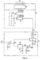
- Figure 1 shows a circuit arrangement comprising the invention, which can be installed, for example, in a hearing aid. It comprises a microphone 1 as an acoustic input converter, which converts acoustic input signals SE, SR into electrical signals SO, an acoustic output converter 2 (which is designed either as a loudspeaker or, particularly in the case of hearing aids, as a so-called receiver), a power amplifier 3 connected upstream of the output converter 2 and a vibration suppressing circuit 4.
- a microphone 1 as an acoustic input converter, which converts acoustic input signals SE, SR into electrical signals SO
- an acoustic output converter 2 which is designed either as a loudspeaker or, particularly in the case of hearing aids, as a so-called receiver
- a power amplifier 3 connected upstream of the output converter 2 and a vibration suppressing circuit 4.
- the vibration suppression circuit 4 is designed as an electrical feedback circuit. It suppresses electrical signals which are generated due to acoustic feedback effects and which generally lead to undamped vibrations in the circuit.
- the feedback effect is indicated in FIG. 1 with a dashed arrow line between acoustic output transducer 2 and microphone 1.
- An acoustic useful signal SE together with an acoustic feedback signal SR is converted into a corresponding electrical signal S0 in the microphone 1.
- the output signal S5 of the vibration suppression circuit 4 is subtracted from this signal S0 in a subtractor 5 from the signal S0.
- the remaining signal S1 is amplified in a non-inverting power amplifier 3 to a signal S2.
- the signal S2 is converted back into an acoustic signal SA in the output converter 2.
- the signal S2 is fed to the vibration suppression circuit 4 as an input signal.
- the vibration suppression circuit 4 consists, functionally broken down, of a vibration detection circuit 6 according to the present invention, a vibration frequency search circuit 7 and an influencing circuit 8.
- the input signal S2 is passed to the vibration detection circuit 6. It is also fed to the influencing circuit 8.
- the vibration detection circuit 6 it is checked whether the signal S2 contains a vibration based on acoustic feedback effects. If an oscillation is present, an oscillation detection signal S3 is emitted.
- the signal S3 sets the oscillation frequency search circuit 7 into operation, a sequence of signals S4 being emitted by the oscillation frequency search circuit 7 until the oscillation detection signal S3 at the output of the oscillation detection circuit 6 disappears.
- the Vibration detection signal S3 at the output of the oscillation frequency search circuit 7 signal S4 is held by the search circuit 7 until a new oscillation occurs.
- the signals S4 control the influencing circuit 8 in the sense that frequency ranges, which are to be assigned to a detected oscillation, are largely suppressed in the entire captured frequency spectrum of the signal S0 by means of a filter.
- the output signal S5 of the influencing circuit 8 is the output signal of the vibration suppression circuit 4.
- FIG. 2 shows a vibration detection circuit 6 designed according to the invention and implemented with analog components. Since vibrations are long-lasting AC voltages with a large amplitude and relatively high frequency, the vibration detection circuit 6 checks the input signal S2 for these properties. In a first stage, the amplitude of the input signal S2 is compared with a first threshold value UT1 by means of a first comparator 9. If the amplitude of S2 exceeds the threshold value UT1, an exceeding signal S21 is produced which is designed as a square wave voltage with time intervals t0 to t n . (The signals S2 and S21 as well as the further evaluation signals S22, S23, S24, which are processed and passed on by the vibration detection circuit 6, are shown in the pulse diagram of FIG. 3).
- the subsequent stage comprises, as the first comparator, an RC element with an ohmic resistor 10, diode 10 ⁇ and capacitor 11 and a second comparator 12.
- the capacitor 11 is quickly charged by the exceeding signal S21 via the diode 10 ⁇ and with a predetermined time constant via the resistor 10 unload. This charge and discharge signal is identified in FIGS. 2 and 3 by S22.
- the time constant together with the threshold value UT2 of the second comparator 12, determines a first time interval TI1, which defines the minimum frequency to which the vibration detection circuit 6 responds. Will one selected small time constant, then the vibration detection circuit 6 responds essentially only to high-frequency signals. With low-frequency signals, the capacitor 11 has sufficient time to discharge below the threshold value UT2 of the second comparator 12. These low-frequency signals are therefore not detected. This ensures that the oscillation detection circuit 6 only reacts to signals that result from acoustic feedback effects, while portions of the useful signal (eg voice signal) that occur periodically at a lower frequency are not taken into account.
- overshoot signals S23 are released to a second comparator 13 to 16.
- the overshoot duration signals S23 are square-wave voltages which have the same duration as the threshold value overshoots of the charge and discharge signals S22.
- the overshoot duration signals S23 thus reflect how long a large, high-frequency input signal lasts (T1).
- the second comparator comprises a diode 13, an RC element 14, 15 and a third comparator 16. With the overshoot signal S23, the capacitor 15 is charged via the resistor 14. Resistor 14 and capacitor 15 are dimensioned so that the charging time constant is large, e.g. 0.5 to 2 seconds.
- the capacitor 15 If the overshoot time signal S23 drops only briefly, the capacitor 15 is immediately completely discharged via the diode 13. However, if the overrun duration signal S23 lasts longer than a predetermined second time interval TI2, the capacitor 15 charges up to such an extent that the voltage exceeds the threshold value UT3 of the subsequent third comparator 16. In this case, the input signal S2 fulfills all vibration detection criteria and the signal S3 emitted by the comparator 16 is regarded as a vibration detection signal.
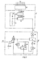
- FIG. 4 shows an oscillation frequency search circuit 7.
- the oscillation frequency search circuit 7 is between the oscillation detection circuit 6 and influencing circuit 8 arranged and controls the influencing circuit 8 such that detected vibrations are suppressed.
- a first device 17 of the search circuit 7 generates digital frequency-determining signals S33 and is controlled by the vibration detection signals S3.
- the main component of the first device 17 is a counting device 18, which comprises a counter 19, a counting direction switch 20 and a reset element 21, also called "power-on reset".
- the first device 17 comprises an oscillator 22 and an associated AND gate 23.
- the counter 19 also serves as a holding device for the frequencies of the detected vibration, as will be explained in more detail below.
- the reset element 21 ensures that the output signals S32 on all four output lines of the counter 19 are in the zero state (also referred to as the “low” state).
- This 0000 value is digitally incremented by one each time a step pulse S31 ("high” state) is registered at the input of the counter 19. After all four output lines have been switched to "high”, the original zero state is restored at the next step pulse S31 and the step sequence is repeated.
- a pulse S31 is only generated if a vibration detection pulse S3 is present at the AND gate 23 connected upstream of the counter 19. If this is the case, then the pulses S31 'generated by means of oscillator 22 are forwarded as step pulses S31. The oscillator 22 therefore determines the speed at which the counter 19 is advanced.
- the counter 19 continues to switch the output pulses S32 until the vibration detection signal S3 disappears. (Signal S3 disappears when the oscillation has been suppressed by the influencing circuit 8). When signal S3 disappears, counter 19 receives no further pulses S31 and remains in the set state until a new one Vibration detection signal S3 occurs.
- the counter 19 thus stores the set state and therefore, together with the AND gate 23, serves as a holding device for holding the frequency of the detected vibration at the influencing circuit 8. It is advantageous to design the oscillation frequency search circuit 7 as a holding device, since the vibration suppression circuit 4 does not drift can and a return of the suppressed vibration is avoided.
- the first device 17 also includes a counting direction switch 20 at the output of the counter 19. This has the effect that a sudden change in the digital frequency-determining signals S33 from 111 to 000 is avoided by counting down every second sequence by inversion of the output pulses S32 from 111 to 000 becomes. This is advantageous in that the filter arranged in the influencing circuit 8 for suppressing the oscillation frequency when the counting direction is reversed does not jump from one end to the other end of the frequency spectrum, but instead moves back and forth in the frequency spectrum.
- a second device 24 of the oscillation frequency search circuit 7 samples the frequency-determining signals S33 of the first device 17 (output of the counting direction switch 20) and controls the influencing circuit 8 via the control signals S4.
- a decoder 25 transmits the eight signal possibilities arriving via three lines to eight different lines. These eight control signals S4 control the influencing circuit 8 in the sense that they determine which frequency range in the controllable frequency spectrum is filtered by the influencing circuit 8.
- the decoder 25 controls the influencing circuit 8 by means of a discretely variable resistor 26.
- the resistance values of the resistors 28 are preferably selected so that the influencing circuit 8 drives eight adjacent frequency ranges within the band 1 kHz to infinity. It is also advantageous if at least one transistor-resistor combination makes it possible to control a frequency range above the acoustic limit of human hearing, so that only this range is filtered after the device is switched on and before an oscillation occurs.
- the influencing circuit 8 also comprises further ohmic resistors 30, capacitors 31 and an amplifier 32, which are arranged in the form of a bandpass filter.
- a bandpass filter is e.g. known from the book "Semiconductor Circuit Technology” by Tietze and Schenk (Springer-Verlag Berlin, Heidelberg, 7th edition (1985), pages 419-421). Since the bandpass filter is designed as a negative feedback of the power amplifier 3, the circuit 8 simulates a notch filter, which forms a suction circuit at the resonance frequency. The bandwidth and gain of the filter are independent of the discretely variable resistor 26. The resonance frequency can thus be varied by changing the resistance values in the resistor 26 without influencing the bandwidth or amplification.
- the output resistor 33 determines the weight of the feedback S5 on the subtractor 5 (see FIG. 1).
- the circuit 8 could be designed as a CR high-pass filter, phase shifter, phase switch or gain reducer.
- Figure 6 shows e.g. a variant 6 ⁇ of the oscillation detection circuit 6 and a variant 7 ⁇ of the oscillation frequency search circuit 7.
- the second comparator 13 to 16 of the oscillation detection circuit 6 is replaced by a digital arrangement which comprises an inverter 34, a digital counter 35 and an AND gate 36.
- the input signal is checked in the same way as in the exemplary embodiment corresponding to FIG. 2 according to the vibration characteristics "large amplitude" and "high frequencies".
- an overshoot signal S23 is processed digitally in order to determine whether the large, high-frequency input signal is long-lasting.
- the counter 35 has two signal inputs: an input for the overshoot signal S21 and a reset input which, together with the inverter 34, continuously resets the counter 35 to the zero state, except when an overshoot signal S23 occurs.
- the counter 35 counts the overshoot signals S21. After a certain number of exceeding signals S21 has occurred, the input signal is regarded as a recognized oscillation.
- the counter 35 then generates, together with the AND gate 36, vibration detection signals S3.
- These vibration detection signals S3 are indexing pulses and can be given directly to the counter 19 of the search circuit 7 ⁇ . This circuit variant therefore does not require an oscillator 22 in the oscillation frequency search circuit.
- FIG. 7 shows a further modification of the circuits in FIGS. 2 and 4, in which the first and second comparison elements (10 to 12, 13 to 16) are replaced by digital arrangements.
- the counter 37 is reset to a 000 level each time an exceeding signal S21 occurs. This process corresponds to a rapid charging of the capacitor 11 in the analog variant of FIG. 2.
- the counter 37 the output Q of which is in the "low” state, begins in the direction of a second one To count the counter reading at a speed predetermined by the oscillator 38. This counting process corresponds to the discharge of the capacitor 11 in the analog variant.
- the "low" state at the output Q of the counter 37 is converted by means of an inverter 39 into a "high” state at the input of the AND gate 40, as a result of which the indexing pulses of the oscillator 38 are passed on. If a further exceeding signal S21 arrives before the counter 37 reaches its second counter reading, the output Q of the counter 37 remains at “low”. However, when the counter 37 reaches the second counter reading, the output Q of the counter 37 is switched to "high” and the AND gate 40 blocks the switching pulses of the oscillator 38. Reaching the second counter reading corresponds to discharging the capacitor 11 up to the threshold value UT2 in Figure 3.
- the counter 35 measures according to the second comparator 13 to 16 of the analog variant, the time duration T 1 of a series of successive exceeding signals S21.
- This counter 35 is only reset to a 000 state if there is no exceeding signal S21 at the AND gate 41: as soon as an exceeding signal S21 occurs, both inputs of the AND gate 41 are switched to a "high” state, which is what Reset input of counter 35 results in a "low” state.
- the counter 35 counts by means of switching pulses from the oscillator 38 until the exceeding signals S21 disappear or until a predetermined, very high counter reading is reached. The very high meter reading is comparable to the slow charging of the capacitor 15 up to a threshold value UT3 in the analog variant. Vibration detection signals S3 are generated by counter 35 as in the modification described above (see FIG. 6).
Landscapes
- Health & Medical Sciences (AREA)
- General Health & Medical Sciences (AREA)
- Neurosurgery (AREA)
- Otolaryngology (AREA)
- Physics & Mathematics (AREA)
- Engineering & Computer Science (AREA)
- Acoustics & Sound (AREA)
- Signal Processing (AREA)
- Control Of Motors That Do Not Use Commutators (AREA)
- Control Of Driving Devices And Active Controlling Of Vehicle (AREA)
- Glass Compositions (AREA)
- Measurement Of Mechanical Vibrations Or Ultrasonic Waves (AREA)
- Filters And Equalizers (AREA)
- Circuit For Audible Band Transducer (AREA)
- Amplifiers (AREA)
- Inductance-Capacitance Distribution Constants And Capacitance-Resistance Oscillators (AREA)
- Analogue/Digital Conversion (AREA)
Claims (13)
- Montage pour détecter des oscillations sur la base d'effets de réaction acoustique, comportant un dispositif à comparateurs à valeur de seuil, qui, lorsque l'amplitude d'un signal d'entrée (S2) dépasse une voleur de seuil d'amplitude prédéterminée, produit des signaux de dépassement (S21) pendant la durée du dépassement de la valeur de seuil, caractérisé par- un premier comparateur à valeur de seuil (9) servant à évaluer l'amplitude des signaux d'entrée (S2),- un premier circuit comparateur constitué par un second comparateur à valeur de seuil (12) possédant une valeur de seuil d'amplitude (UT2) et un dispositif de charge et de décharge (10,10',11) servant à détecter les intervalles de temps (t₀ à tn) entre les différents signaux, et- un second circuit comparateur constitué par un troisième comparateur à valeur de seuil (16) possédant une valeur de seuil d'amplitude (UT3) et un dispositif de charge et de décharge (13,14,15) servant à détecter la durée de temps (T₁) d'un groupe de signaux, lorsqu'une série de signaux d'entrée (S2) se succèdent très près les uns des autres.
- Montage suivant la revendication 1, caractérisé par le fait que le premier circuit comparateur (10 à 12; 37 à 40) délivre un signal de durée de dépassement (S23) tant que les intervalles de temps (t₀ à tn) entre des signaux individuels dépassent un premier intervalle de temps prédéterminé (TI1), et que le second circuit comparateur (13 à 16; 34 à 36, 38, 41) délivre un signal d'identification d'oscillation (S3) tant que le signal de durée de dépassement (S23) dépasse un second intervalle de temps prédéterminé (TI2).
- Montage suivant les revendications 1 et 2, caractérisé par le fait qu'à la sortie du premier comparateur à valeur de seuil (9), qui produit des signaux de dépassement (S21), du dispositif à comparateurs à valeur de seuil, le second comparateur à valeur de seuil (12) est branché en tant que premier circuit comparateur, dont le dispositif de charge et de décharge (10, 10', 11) peut être chargé lors de l'apparition des signaux de dépassement (S21) et peut être déchargé avec une première constante de temps prédéterminée pendant les intervalles de temps s'étendant entre les signaux de dépassement (S21) et les signaux de charge et de décharge (S22) produits peuvent être comparés, par le circuit comparateur, à la valeur de seuil d'amplitude (UT2) du second comparateur à valeur de seuil (12), auquel cas un signal de durée de dépassement (S23) est produit pendant la durée du dépassement de la valeur de seuil d'amplitude (UT2) du second comparateur à valeur de seuil (12).
- Montage suivant les revendications 1 à 3, caractérisé par le fait que le troisième comparateur à valeur de seuil (16) est branché à la sortie du second comparateur à valeur de seuil (12), en tant que circuit servant à évaluer une série de dépassements successifs et dont le dispositif de charge et de décharge (13 à 15) peut être chargé avec une seconde constante de temps prédéterminée, pendant la durée de l'apparition d'un signal de durée de dépassement (S23) et peut être déchargé à la fin de chaque signal de durée de dépassement, et que le troisième comparateur à valeur de seuil (16) produit le signal d'identification d'oscillation (S3) lorsque le signal de charge et de décharge (S24) du dispositif de charge et de décharge (13 à 15) dépasse la valeur de seuil d'amplitude (UT3) du troisième comparateur à valeur de seuil (16).
- Montage suivant les revendications 1 à 4, caractérisé par le fait que l'intervalle de temps respectif (TI1; TI2) est prédéterminé par une constante de temps en liaison avec une valeur de seuil (UT2,UT3).
- Montage suivant les revendications 1 à 5, caractérisé par le fait que le premier intervalle de temps (TI1) est prédéterminé par la constante de temps d'un dispositif de décharge (10, 11; 37, 38) pour les signaux de dépassement (S21), après une charge préalable dans un dispositif de charge (10', 11; 37) et que la valeur de seuil (UT2) est celle d'un comparateur à valeur de seuil (12; 37, 40) qui est prévu pour des signaux de charge et de décharge (22).
- Montage suivant l'une des revendications 1 à 5, caractérisé par le fait que le second intervalle de temps est prédéterminé par la constante de temps d'un dispositif de charge (14, 15; 35, 38) pour les signaux de durée de dépassement (S23) et la valeur de seuil (UT3) est celle d'un comparateur à valeur de seuil (16; 35, 41) pour les signaux de charge (S24) des signaux de durée de dépassement.
- Montage suivant l'une des revendications 6 ou 7, caractérisé par le fait que le dispositif de charge ou de décharge (10 à 11, 13 à 15) comporte un condensateur (11, 15), qui détermine la constante de temps conjointement avec une résistance de charge ou de décharge (10, 14).
- Montage suivant la revendication 8, caractérisé par le fait que la valeur de seuil est un signal analogique qui peut être comparé au signal de charge et de décharge du condensateur (11, 15).
- Montage suivant la revendication 6 ou 7, caractérisé par le fait que le dispositif de charge ou de décharge (35, 37, 38) comprend un compteur (35, 37), dont la vitesse de comptage est déterminée par la constante de temps.
- Montage suivant la revendication 10, caractérisé par le fait que la valeur de seuil est prédéterminée par un état de comptage.
- Montage suivant l'une des revendications 6, 10 ou 11, caractérisé par le fait qu'à la sortie d'un comparateur à valeur de seuil (9) qui produit les signaux de dépassement (S21), est branché un premier compteur (37) en tant que circuit qui sert à évaluer les intervalles de temps (t₀ à tn) entre les signaux de dépassement, est positionné à un premier état de comptage lors de l'apparition de chaque signal de dépassement (S21), compte en direction d'un second état de comptage en fonction d'impulsions de comptage d'un générateur d'impulsions de comptage (38) et produit le signal de durée de dépassement (S23) jusqu'à ce que le second état de comptage soit atteint.
- Montage suivant la revendication 12, caractérisé par le fait qu'à la sortie du premier compteur (37) est disposé un second compteur (35) en tant que circuit qui sert à évaluer une série de signaux de dépassement successifs (21), est bloqué à un premier état de comptage avant l'apparition d'un signal de durée de dépassement (S23) et compte en direction d'un second état de comptage après l'apparition d'un signal de durée de dépassement, en fonction d'impulsions de comptage d'un générateur d'impulsions de comptage (38) et produit le signal d'identification d'oscillation (S3), lorsque le second compteur (35) atteint le second état de comptage, et ce jusqu'à ce que le second compteur soit ramené au premier état de comptage.
Priority Applications (1)
| Application Number | Priority Date | Filing Date | Title |
|---|---|---|---|
| AT88101634T ATE69132T1 (de) | 1987-02-17 | 1988-02-04 | Schaltungsanordnung zum erkennen von schwingungen. |
Applications Claiming Priority (2)
| Application Number | Priority Date | Filing Date | Title |
|---|---|---|---|
| DE3704998 | 1987-02-17 | ||
| DE3704998 | 1987-02-17 |
Publications (2)
| Publication Number | Publication Date |
|---|---|
| EP0280909A1 EP0280909A1 (fr) | 1988-09-07 |
| EP0280909B1 true EP0280909B1 (fr) | 1991-10-30 |
Family
ID=6321172
Family Applications (1)
| Application Number | Title | Priority Date | Filing Date |
|---|---|---|---|
| EP88101634A Expired - Lifetime EP0280909B1 (fr) | 1987-02-17 | 1988-02-04 | Montage pour la détection d'oscillations |
Country Status (5)
| Country | Link |
|---|---|
| US (1) | US4845757A (fr) |
| EP (1) | EP0280909B1 (fr) |
| AT (1) | ATE69132T1 (fr) |
| DE (1) | DE3865859D1 (fr) |
| DK (1) | DK169012B1 (fr) |
Cited By (1)
| Publication number | Priority date | Publication date | Assignee | Title |
|---|---|---|---|---|
| DE102007007120A1 (de) * | 2007-02-13 | 2008-08-21 | Siemens Audiologische Technik Gmbh | Verfahren zum Erzeugen von akustischen Signalen eines Hörgeräts |
Families Citing this family (20)
| Publication number | Priority date | Publication date | Assignee | Title |
|---|---|---|---|---|
| US5225836A (en) * | 1988-03-23 | 1993-07-06 | Central Institute For The Deaf | Electronic filters, repeated signal charge conversion apparatus, hearing aids and methods |
| US5091952A (en) * | 1988-11-10 | 1992-02-25 | Wisconsin Alumni Research Foundation | Feedback suppression in digital signal processing hearing aids |
| US5259033A (en) * | 1989-08-30 | 1993-11-02 | Gn Danavox As | Hearing aid having compensation for acoustic feedback |
| JPH06503897A (ja) * | 1990-09-14 | 1994-04-28 | トッドター、クリス | ノイズ消去システム |
| US5134658A (en) * | 1990-09-27 | 1992-07-28 | Advanced Micro Devices, Inc. | Apparatus for discriminating information signals from noise signals in a communication signal |
| DK0567535T3 (da) * | 1991-01-17 | 2003-12-08 | Roger A Adelman | Forbedret høreapparat |
| US5621802A (en) * | 1993-04-27 | 1997-04-15 | Regents Of The University Of Minnesota | Apparatus for eliminating acoustic oscillation in a hearing aid by using phase equalization |
| US5412734A (en) * | 1993-09-13 | 1995-05-02 | Thomasson; Samuel L. | Apparatus and method for reducing acoustic feedback |
| US5533120A (en) * | 1994-02-01 | 1996-07-02 | Tandy Corporation | Acoustic feedback cancellation for equalized amplifying systems |
| JP2773678B2 (ja) * | 1994-09-09 | 1998-07-09 | ヤマハ株式会社 | ハウリング防止装置 |
| US6466678B1 (en) | 1994-11-30 | 2002-10-15 | Etymotic Research, Inc. | Hearing aid having digital damping |
| US5812679A (en) * | 1994-11-30 | 1998-09-22 | Killion; Mead | Electronic damper circuit for a hearing aid and a method of using the same |
| GB2311186A (en) * | 1996-03-13 | 1997-09-17 | Jan Albert Gadd | Hearing aid feedback detecting and warning device |
| US6252967B1 (en) * | 1999-01-21 | 2001-06-26 | Acoustic Technologies, Inc. | Reducing acoustic feedback with digital modulation |
| US6480610B1 (en) * | 1999-09-21 | 2002-11-12 | Sonic Innovations, Inc. | Subband acoustic feedback cancellation in hearing aids |
| DE10244184B3 (de) * | 2002-09-23 | 2004-04-15 | Siemens Audiologische Technik Gmbh | Feedbackkompensation für Hörgeräte mit Systemabstandsschätzung |
| US7756276B2 (en) * | 2003-08-20 | 2010-07-13 | Phonak Ag | Audio amplification apparatus |
| AU2004201374B2 (en) * | 2004-04-01 | 2010-12-23 | Phonak Ag | Audio amplification apparatus |
| AU2003236382B2 (en) * | 2003-08-20 | 2011-02-24 | Phonak Ag | Feedback suppression in sound signal processing using frequency transposition |
| US20070106530A1 (en) * | 2004-05-26 | 2007-05-10 | Blamey Peter J | Oscillation suppression |
Family Cites Families (5)
| Publication number | Priority date | Publication date | Assignee | Title |
|---|---|---|---|---|
| US4054462A (en) * | 1976-03-01 | 1977-10-18 | The Dow Chemical Company | Method of cementing |
| US4091236A (en) * | 1976-09-07 | 1978-05-23 | The University Of Akron | Automatically tunable notch filter and method for suppression of acoustical feedback |
| NL7612358A (nl) * | 1976-11-08 | 1978-05-10 | Philips Nv | Versterkerinrichting voor akoestische signalen voorzien van middelen voor het onderdrukken van ongewenste stoorsignalen. |
| US4079199A (en) * | 1977-05-25 | 1978-03-14 | Patronis Jr Eugene T | Acoustic feedback detector and automatic gain control |
| US4232192A (en) * | 1978-05-01 | 1980-11-04 | Starkey Labs, Inc. | Moving-average notch filter |
-
1988
- 1988-02-04 EP EP88101634A patent/EP0280909B1/fr not_active Expired - Lifetime
- 1988-02-04 US US07/152,390 patent/US4845757A/en not_active Expired - Fee Related
- 1988-02-04 AT AT88101634T patent/ATE69132T1/de not_active IP Right Cessation
- 1988-02-04 DE DE8888101634T patent/DE3865859D1/de not_active Expired - Lifetime
- 1988-02-16 DK DK077988A patent/DK169012B1/da not_active IP Right Cessation
Cited By (1)
| Publication number | Priority date | Publication date | Assignee | Title |
|---|---|---|---|---|
| DE102007007120A1 (de) * | 2007-02-13 | 2008-08-21 | Siemens Audiologische Technik Gmbh | Verfahren zum Erzeugen von akustischen Signalen eines Hörgeräts |
Also Published As
| Publication number | Publication date |
|---|---|
| DE3865859D1 (de) | 1991-12-05 |
| EP0280909A1 (fr) | 1988-09-07 |
| US4845757A (en) | 1989-07-04 |
| DK77988A (da) | 1988-08-18 |
| DK77988D0 (da) | 1988-02-16 |
| DK169012B1 (da) | 1994-07-25 |
| ATE69132T1 (de) | 1991-11-15 |
Similar Documents
| Publication | Publication Date | Title |
|---|---|---|
| EP0280909B1 (fr) | Montage pour la détection d'oscillations | |
| DE2104779C3 (de) | Bandfilter-Schaltung | |
| DE69926851T2 (de) | Verfahren und Vorrichtung zur Sprachaktivitätsdetektion | |
| DE60028779T2 (de) | Rückkopplungsanullierung mit niederfrequenzeingang | |
| DE69223147T2 (de) | Lärmdämpfsystem | |
| DE2747821C2 (de) | Verstärkeranordnung für akustische Signale mit Mitteln zum Unterdrücken unerwünschter Störsignale | |
| DE3802903A1 (de) | Einrichtung zur uebertragung von sprache | |
| DE2355700C3 (de) | Frequenzumschaltbarer Tonfrequenzdetektor | |
| DE2658301B1 (de) | Hoergeraet | |
| EP0280907B1 (fr) | Montage pour la suppression d'oscillations | |
| DE69718975T2 (de) | Verbesserungen in oder in bezug auf elektronische Filter | |
| DE2813628A1 (de) | Filterschaltung | |
| DE69217853T2 (de) | Tondetektor mit Nullspannungsübergangsdetektor | |
| EP1052881B1 (fr) | Prothèse acoustique avec détecteur d'oscillations et méthode de détection d'oscillations dans une prothèse acoustique | |
| DE3227087C2 (de) | Bandfilterverstärkerschaltung | |
| EP0182742A1 (fr) | Circuit de production d'un critère de réception | |
| DE2758476C2 (fr) | ||
| EP1458216A2 (fr) | Appareil et procédé à l'adaption de microphones dans une prothèse auditive | |
| DE3606973A1 (de) | Schaltungsanordnung fuer ein freisprechtelefon | |
| DE3602585A1 (de) | Filter | |
| DE69208602T2 (de) | Ein den Frequenzhub begrenzender Übertragungsschaltkreis | |
| DE2849374C2 (fr) | ||
| DE1148591B (de) | Taktfrequenz-Generatoranordnung fuer Impulskodemodulations-Systeme | |
| DE4125379C1 (en) | Hearing aid device with amplitude limitation - has limiting circuit inserted in feedback path for amplifier stage for matching frequency characteristic to each individual user | |
| DE3027715C2 (de) | Schaltungsanordnung zur selbsttätigen Regelung oder Begrenzung der Dynamik von Signalen |
Legal Events
| Date | Code | Title | Description |
|---|---|---|---|
| PUAI | Public reference made under article 153(3) epc to a published international application that has entered the european phase |
Free format text: ORIGINAL CODE: 0009012 |
|
| AK | Designated contracting states |
Kind code of ref document: A1 Designated state(s): AT CH DE FR GB IT LI NL |
|
| 17P | Request for examination filed |
Effective date: 19880923 |
|
| 17Q | First examination report despatched |
Effective date: 19900808 |
|
| GRAA | (expected) grant |
Free format text: ORIGINAL CODE: 0009210 |
|
| AK | Designated contracting states |
Kind code of ref document: B1 Designated state(s): AT CH DE FR GB IT LI NL |
|
| PG25 | Lapsed in a contracting state [announced via postgrant information from national office to epo] |
Ref country code: IT Free format text: LAPSE BECAUSE OF FAILURE TO SUBMIT A TRANSLATION OF THE DESCRIPTION OR TO PAY THE FEE WITHIN THE PRE;WARNING: LAPSES OF ITALIAN PATENTS WITH EFFECTIVE DATE BEFORE 2007 MAY HAVE OCCURRED AT ANY TIME BEFORE 2007. THE CORRECT EFFECTIVE DATE MAY BE DIFFERENT FROM THE ONE RECORDED.SCRIBED TIME-LIMIT Effective date: 19911030 Ref country code: GB Effective date: 19911030 |
|
| REF | Corresponds to: |
Ref document number: 69132 Country of ref document: AT Date of ref document: 19911115 Kind code of ref document: T |
|
| REF | Corresponds to: |
Ref document number: 3865859 Country of ref document: DE Date of ref document: 19911205 |
|
| ET | Fr: translation filed | ||
| GBV | Gb: ep patent (uk) treated as always having been void in accordance with gb section 77(7)/1977 [no translation filed] | ||
| PLBE | No opposition filed within time limit |
Free format text: ORIGINAL CODE: 0009261 |
|
| STAA | Information on the status of an ep patent application or granted ep patent |
Free format text: STATUS: NO OPPOSITION FILED WITHIN TIME LIMIT |
|
| 26N | No opposition filed | ||
| PGFP | Annual fee paid to national office [announced via postgrant information from national office to epo] |
Ref country code: AT Payment date: 19930127 Year of fee payment: 6 |
|
| PG25 | Lapsed in a contracting state [announced via postgrant information from national office to epo] |
Ref country code: AT Effective date: 19940204 |
|
| PGFP | Annual fee paid to national office [announced via postgrant information from national office to epo] |
Ref country code: FR Payment date: 19940224 Year of fee payment: 7 |
|
| PGFP | Annual fee paid to national office [announced via postgrant information from national office to epo] |
Ref country code: NL Payment date: 19940228 Year of fee payment: 7 |
|
| PG25 | Lapsed in a contracting state [announced via postgrant information from national office to epo] |
Ref country code: NL Effective date: 19950901 |
|
| PG25 | Lapsed in a contracting state [announced via postgrant information from national office to epo] |
Ref country code: FR Effective date: 19951031 |
|
| NLV4 | Nl: lapsed or anulled due to non-payment of the annual fee |
Effective date: 19950901 |
|
| REG | Reference to a national code |
Ref country code: FR Ref legal event code: ST |
|
| PGFP | Annual fee paid to national office [announced via postgrant information from national office to epo] |
Ref country code: DE Payment date: 19990419 Year of fee payment: 12 |
|
| PGFP | Annual fee paid to national office [announced via postgrant information from national office to epo] |
Ref country code: CH Payment date: 19990514 Year of fee payment: 12 |
|
| PG25 | Lapsed in a contracting state [announced via postgrant information from national office to epo] |
Ref country code: LI Free format text: LAPSE BECAUSE OF NON-PAYMENT OF DUE FEES Effective date: 20000229 Ref country code: CH Free format text: LAPSE BECAUSE OF NON-PAYMENT OF DUE FEES Effective date: 20000229 |
|
| REG | Reference to a national code |
Ref country code: CH Ref legal event code: PL |
|
| PG25 | Lapsed in a contracting state [announced via postgrant information from national office to epo] |
Ref country code: DE Free format text: LAPSE BECAUSE OF NON-PAYMENT OF DUE FEES Effective date: 20001201 |