EP0280909B1 - Circuit arrangement for the detection of oscillations - Google Patents
Circuit arrangement for the detection of oscillations Download PDFInfo
- Publication number
- EP0280909B1 EP0280909B1 EP88101634A EP88101634A EP0280909B1 EP 0280909 B1 EP0280909 B1 EP 0280909B1 EP 88101634 A EP88101634 A EP 88101634A EP 88101634 A EP88101634 A EP 88101634A EP 0280909 B1 EP0280909 B1 EP 0280909B1
- Authority
- EP
- European Patent Office
- Prior art keywords
- threshold value
- signal
- exceeding
- signals
- charge
- Prior art date
- Legal status (The legal status is an assumption and is not a legal conclusion. Google has not performed a legal analysis and makes no representation as to the accuracy of the status listed.)
- Expired - Lifetime
Links
Images


Classifications
-
- H—ELECTRICITY
- H04—ELECTRIC COMMUNICATION TECHNIQUE
- H04R—LOUDSPEAKERS, MICROPHONES, GRAMOPHONE PICK-UPS OR LIKE ACOUSTIC ELECTROMECHANICAL TRANSDUCERS; DEAF-AID SETS; PUBLIC ADDRESS SYSTEMS
- H04R25/00—Deaf-aid sets, i.e. electro-acoustic or electro-mechanical hearing aids; Electric tinnitus maskers providing an auditory perception
- H04R25/45—Prevention of acoustic reaction, i.e. acoustic oscillatory feedback
- H04R25/453—Prevention of acoustic reaction, i.e. acoustic oscillatory feedback electronically
-
- H—ELECTRICITY
- H04—ELECTRIC COMMUNICATION TECHNIQUE
- H04R—LOUDSPEAKERS, MICROPHONES, GRAMOPHONE PICK-UPS OR LIKE ACOUSTIC ELECTROMECHANICAL TRANSDUCERS; DEAF-AID SETS; PUBLIC ADDRESS SYSTEMS
- H04R25/00—Deaf-aid sets, i.e. electro-acoustic or electro-mechanical hearing aids; Electric tinnitus maskers providing an auditory perception
- H04R25/50—Customised settings for obtaining desired overall acoustical characteristics
- H04R25/505—Customised settings for obtaining desired overall acoustical characteristics using digital signal processing
Definitions
- the present invention relates to a circuit arrangement according to the preamble of patent claim 1.
- Circuits have recently been developed (for example by RIM-Elektronik, Kunststoff, and US Pat. No. 4,232,192) which recognize vibrations as such and then suppress them.
- Such circuits tap the useful signal between the input converter and a power amplifier connected upstream of the output converter and amplify it by means of an additional amplifier.
- the amplified signal is compared in a comparator stage with a threshold voltage and fed into a phase locked loop (so-called phase locked loop or PLL for short).
- An input signal is evaluated as a vibration if it exceeds an amplitude threshold specified by a comparator.
- the PLL is activated when all thresholds are exceeded.
- the PLL then "searches" for the frequency of the overshoot signal and outputs a suppression signal to a notch filter connected upstream of the power amplifier, which suppresses the frequency range of the overshoot signal.
- the object of the present invention is to construct a vibration detection circuit which only emits a vibration detection signal when the input signal has been assessed as positive in a plurality of test processes, so that incorrect evaluations in the vibration detection circuit are avoided.
- the vibration detection circuit comprises elements which test the useful signal with regard to three vibration characteristics. Since vibrations are long-lasting AC voltages with a large amplitude and relatively high frequency, the vibration detection circuit checks the amplitude size of the input signals, the time interval between individual signal swings (frequency) and the duration of a series of successive signal swings (group length).
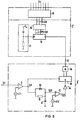
- Figure 1 shows a circuit arrangement comprising the invention, which can be installed, for example, in a hearing aid. It comprises a microphone 1 as an acoustic input converter, which converts acoustic input signals SE, SR into electrical signals SO, an acoustic output converter 2 (which is designed either as a loudspeaker or, particularly in the case of hearing aids, as a so-called receiver), a power amplifier 3 connected upstream of the output converter 2 and a vibration suppressing circuit 4.
- a microphone 1 as an acoustic input converter, which converts acoustic input signals SE, SR into electrical signals SO
- an acoustic output converter 2 which is designed either as a loudspeaker or, particularly in the case of hearing aids, as a so-called receiver
- a power amplifier 3 connected upstream of the output converter 2 and a vibration suppressing circuit 4.
- the vibration suppression circuit 4 is designed as an electrical feedback circuit. It suppresses electrical signals which are generated due to acoustic feedback effects and which generally lead to undamped vibrations in the circuit.
- the feedback effect is indicated in FIG. 1 with a dashed arrow line between acoustic output transducer 2 and microphone 1.
- An acoustic useful signal SE together with an acoustic feedback signal SR is converted into a corresponding electrical signal S0 in the microphone 1.
- the output signal S5 of the vibration suppression circuit 4 is subtracted from this signal S0 in a subtractor 5 from the signal S0.
- the remaining signal S1 is amplified in a non-inverting power amplifier 3 to a signal S2.
- the signal S2 is converted back into an acoustic signal SA in the output converter 2.
- the signal S2 is fed to the vibration suppression circuit 4 as an input signal.
- the vibration suppression circuit 4 consists, functionally broken down, of a vibration detection circuit 6 according to the present invention, a vibration frequency search circuit 7 and an influencing circuit 8.
- the input signal S2 is passed to the vibration detection circuit 6. It is also fed to the influencing circuit 8.
- the vibration detection circuit 6 it is checked whether the signal S2 contains a vibration based on acoustic feedback effects. If an oscillation is present, an oscillation detection signal S3 is emitted.
- the signal S3 sets the oscillation frequency search circuit 7 into operation, a sequence of signals S4 being emitted by the oscillation frequency search circuit 7 until the oscillation detection signal S3 at the output of the oscillation detection circuit 6 disappears.
- the Vibration detection signal S3 at the output of the oscillation frequency search circuit 7 signal S4 is held by the search circuit 7 until a new oscillation occurs.
- the signals S4 control the influencing circuit 8 in the sense that frequency ranges, which are to be assigned to a detected oscillation, are largely suppressed in the entire captured frequency spectrum of the signal S0 by means of a filter.
- the output signal S5 of the influencing circuit 8 is the output signal of the vibration suppression circuit 4.
- FIG. 2 shows a vibration detection circuit 6 designed according to the invention and implemented with analog components. Since vibrations are long-lasting AC voltages with a large amplitude and relatively high frequency, the vibration detection circuit 6 checks the input signal S2 for these properties. In a first stage, the amplitude of the input signal S2 is compared with a first threshold value UT1 by means of a first comparator 9. If the amplitude of S2 exceeds the threshold value UT1, an exceeding signal S21 is produced which is designed as a square wave voltage with time intervals t0 to t n . (The signals S2 and S21 as well as the further evaluation signals S22, S23, S24, which are processed and passed on by the vibration detection circuit 6, are shown in the pulse diagram of FIG. 3).
- the subsequent stage comprises, as the first comparator, an RC element with an ohmic resistor 10, diode 10 ⁇ and capacitor 11 and a second comparator 12.
- the capacitor 11 is quickly charged by the exceeding signal S21 via the diode 10 ⁇ and with a predetermined time constant via the resistor 10 unload. This charge and discharge signal is identified in FIGS. 2 and 3 by S22.
- the time constant together with the threshold value UT2 of the second comparator 12, determines a first time interval TI1, which defines the minimum frequency to which the vibration detection circuit 6 responds. Will one selected small time constant, then the vibration detection circuit 6 responds essentially only to high-frequency signals. With low-frequency signals, the capacitor 11 has sufficient time to discharge below the threshold value UT2 of the second comparator 12. These low-frequency signals are therefore not detected. This ensures that the oscillation detection circuit 6 only reacts to signals that result from acoustic feedback effects, while portions of the useful signal (eg voice signal) that occur periodically at a lower frequency are not taken into account.
- overshoot signals S23 are released to a second comparator 13 to 16.
- the overshoot duration signals S23 are square-wave voltages which have the same duration as the threshold value overshoots of the charge and discharge signals S22.
- the overshoot duration signals S23 thus reflect how long a large, high-frequency input signal lasts (T1).
- the second comparator comprises a diode 13, an RC element 14, 15 and a third comparator 16. With the overshoot signal S23, the capacitor 15 is charged via the resistor 14. Resistor 14 and capacitor 15 are dimensioned so that the charging time constant is large, e.g. 0.5 to 2 seconds.
- the capacitor 15 If the overshoot time signal S23 drops only briefly, the capacitor 15 is immediately completely discharged via the diode 13. However, if the overrun duration signal S23 lasts longer than a predetermined second time interval TI2, the capacitor 15 charges up to such an extent that the voltage exceeds the threshold value UT3 of the subsequent third comparator 16. In this case, the input signal S2 fulfills all vibration detection criteria and the signal S3 emitted by the comparator 16 is regarded as a vibration detection signal.
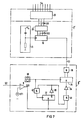
- FIG. 4 shows an oscillation frequency search circuit 7.
- the oscillation frequency search circuit 7 is between the oscillation detection circuit 6 and influencing circuit 8 arranged and controls the influencing circuit 8 such that detected vibrations are suppressed.
- a first device 17 of the search circuit 7 generates digital frequency-determining signals S33 and is controlled by the vibration detection signals S3.
- the main component of the first device 17 is a counting device 18, which comprises a counter 19, a counting direction switch 20 and a reset element 21, also called "power-on reset".
- the first device 17 comprises an oscillator 22 and an associated AND gate 23.
- the counter 19 also serves as a holding device for the frequencies of the detected vibration, as will be explained in more detail below.
- the reset element 21 ensures that the output signals S32 on all four output lines of the counter 19 are in the zero state (also referred to as the “low” state).
- This 0000 value is digitally incremented by one each time a step pulse S31 ("high” state) is registered at the input of the counter 19. After all four output lines have been switched to "high”, the original zero state is restored at the next step pulse S31 and the step sequence is repeated.
- a pulse S31 is only generated if a vibration detection pulse S3 is present at the AND gate 23 connected upstream of the counter 19. If this is the case, then the pulses S31 'generated by means of oscillator 22 are forwarded as step pulses S31. The oscillator 22 therefore determines the speed at which the counter 19 is advanced.
- the counter 19 continues to switch the output pulses S32 until the vibration detection signal S3 disappears. (Signal S3 disappears when the oscillation has been suppressed by the influencing circuit 8). When signal S3 disappears, counter 19 receives no further pulses S31 and remains in the set state until a new one Vibration detection signal S3 occurs.
- the counter 19 thus stores the set state and therefore, together with the AND gate 23, serves as a holding device for holding the frequency of the detected vibration at the influencing circuit 8. It is advantageous to design the oscillation frequency search circuit 7 as a holding device, since the vibration suppression circuit 4 does not drift can and a return of the suppressed vibration is avoided.
- the first device 17 also includes a counting direction switch 20 at the output of the counter 19. This has the effect that a sudden change in the digital frequency-determining signals S33 from 111 to 000 is avoided by counting down every second sequence by inversion of the output pulses S32 from 111 to 000 becomes. This is advantageous in that the filter arranged in the influencing circuit 8 for suppressing the oscillation frequency when the counting direction is reversed does not jump from one end to the other end of the frequency spectrum, but instead moves back and forth in the frequency spectrum.
- a second device 24 of the oscillation frequency search circuit 7 samples the frequency-determining signals S33 of the first device 17 (output of the counting direction switch 20) and controls the influencing circuit 8 via the control signals S4.
- a decoder 25 transmits the eight signal possibilities arriving via three lines to eight different lines. These eight control signals S4 control the influencing circuit 8 in the sense that they determine which frequency range in the controllable frequency spectrum is filtered by the influencing circuit 8.
- the decoder 25 controls the influencing circuit 8 by means of a discretely variable resistor 26.
- the resistance values of the resistors 28 are preferably selected so that the influencing circuit 8 drives eight adjacent frequency ranges within the band 1 kHz to infinity. It is also advantageous if at least one transistor-resistor combination makes it possible to control a frequency range above the acoustic limit of human hearing, so that only this range is filtered after the device is switched on and before an oscillation occurs.
- the influencing circuit 8 also comprises further ohmic resistors 30, capacitors 31 and an amplifier 32, which are arranged in the form of a bandpass filter.
- a bandpass filter is e.g. known from the book "Semiconductor Circuit Technology” by Tietze and Schenk (Springer-Verlag Berlin, Heidelberg, 7th edition (1985), pages 419-421). Since the bandpass filter is designed as a negative feedback of the power amplifier 3, the circuit 8 simulates a notch filter, which forms a suction circuit at the resonance frequency. The bandwidth and gain of the filter are independent of the discretely variable resistor 26. The resonance frequency can thus be varied by changing the resistance values in the resistor 26 without influencing the bandwidth or amplification.
- the output resistor 33 determines the weight of the feedback S5 on the subtractor 5 (see FIG. 1).
- the circuit 8 could be designed as a CR high-pass filter, phase shifter, phase switch or gain reducer.
- Figure 6 shows e.g. a variant 6 ⁇ of the oscillation detection circuit 6 and a variant 7 ⁇ of the oscillation frequency search circuit 7.
- the second comparator 13 to 16 of the oscillation detection circuit 6 is replaced by a digital arrangement which comprises an inverter 34, a digital counter 35 and an AND gate 36.
- the input signal is checked in the same way as in the exemplary embodiment corresponding to FIG. 2 according to the vibration characteristics "large amplitude" and "high frequencies".
- an overshoot signal S23 is processed digitally in order to determine whether the large, high-frequency input signal is long-lasting.
- the counter 35 has two signal inputs: an input for the overshoot signal S21 and a reset input which, together with the inverter 34, continuously resets the counter 35 to the zero state, except when an overshoot signal S23 occurs.
- the counter 35 counts the overshoot signals S21. After a certain number of exceeding signals S21 has occurred, the input signal is regarded as a recognized oscillation.
- the counter 35 then generates, together with the AND gate 36, vibration detection signals S3.
- These vibration detection signals S3 are indexing pulses and can be given directly to the counter 19 of the search circuit 7 ⁇ . This circuit variant therefore does not require an oscillator 22 in the oscillation frequency search circuit.
- FIG. 7 shows a further modification of the circuits in FIGS. 2 and 4, in which the first and second comparison elements (10 to 12, 13 to 16) are replaced by digital arrangements.
- the counter 37 is reset to a 000 level each time an exceeding signal S21 occurs. This process corresponds to a rapid charging of the capacitor 11 in the analog variant of FIG. 2.
- the counter 37 the output Q of which is in the "low” state, begins in the direction of a second one To count the counter reading at a speed predetermined by the oscillator 38. This counting process corresponds to the discharge of the capacitor 11 in the analog variant.
- the "low" state at the output Q of the counter 37 is converted by means of an inverter 39 into a "high” state at the input of the AND gate 40, as a result of which the indexing pulses of the oscillator 38 are passed on. If a further exceeding signal S21 arrives before the counter 37 reaches its second counter reading, the output Q of the counter 37 remains at “low”. However, when the counter 37 reaches the second counter reading, the output Q of the counter 37 is switched to "high” and the AND gate 40 blocks the switching pulses of the oscillator 38. Reaching the second counter reading corresponds to discharging the capacitor 11 up to the threshold value UT2 in Figure 3.
- the counter 35 measures according to the second comparator 13 to 16 of the analog variant, the time duration T 1 of a series of successive exceeding signals S21.
- This counter 35 is only reset to a 000 state if there is no exceeding signal S21 at the AND gate 41: as soon as an exceeding signal S21 occurs, both inputs of the AND gate 41 are switched to a "high” state, which is what Reset input of counter 35 results in a "low” state.
- the counter 35 counts by means of switching pulses from the oscillator 38 until the exceeding signals S21 disappear or until a predetermined, very high counter reading is reached. The very high meter reading is comparable to the slow charging of the capacitor 15 up to a threshold value UT3 in the analog variant. Vibration detection signals S3 are generated by counter 35 as in the modification described above (see FIG. 6).
Abstract
Description
Die vorliegende Erfindung betrifft eine Schaltungsanordnung gemäß Oberbegriff des Patentanspruchs 1.The present invention relates to a circuit arrangement according to the preamble of
Bei elektronischen Geräten, die ein Mikrofon und einen Lautsprecher in unmittelbarer Nähe zueinander umfassen, besteht häufig die Gefahr von akustischen Rückkopplungseffekten. Insbesondere bei Hörgeräten, deren Schallwandler (Mikrofon und Hörer) nur gering voneinander entfernt sind, treten durch dieses Phänomen Töne, z.B. Pfeifen, auf, die störend sind.With electronic devices that include a microphone and a loudspeaker in close proximity to one another, there is often the risk of acoustic feedback effects. In particular in the case of hearing aids, the sound transducers (microphone and receiver) of which are only slightly separated from one another, tones occur due to this phenomenon, e.g. Whistle on, which are bothersome.
Man bemühte sich früher, speziell bei Hörgeräten, hauptsächlich durch Verengung des Hörkanals und Herstellung von schallisolierenden Otoplastiken, die Schwinganfälligkeit zu reduzieren. Elektrische Gegenmaßnahmen beschnitten oder verschoben allenfalls das Frequenzband, anstatt am Schwingungssignal selbst anzugreifen.In the past, efforts were made to reduce the susceptibility to vibrations, particularly in the case of hearing aids, mainly by narrowing the auditory canal and producing sound-insulating earmolds. Electrical countermeasures at most cut or shift the frequency band instead of attacking the vibration signal itself.
In jüngster Zeit sind Schaltungen entwickelt worden (z.B. Firma RIM-Elektronik, München, und US-PS 4,232,192), die Schwingungen als solche erkennen und sie daraufhin unterdrücken. Solche Schaltungen greifen das Nutzsignal zwischen Eingangswandler und einem den Ausgangswandler vorgeschalteten Endverstärker ab und verstärken es mittels eines zusätzlichen Verstärkers. Das verstärkte Signal wird in einer Komparatorstufe mit einer Schwellenspannung verglichen und in einen Phasenregelkreis (sogenannter Phase-Locked-Loop oder abgekürzt PLL) eingespeist. Ein Eingangssignal wird als Schwingung bewertet, wenn es eine mittels Komparator vorgegebene Amplitudenschwelle überschreitet. Bei sämtlichen Schwellenüberschreitungen wird der PLL eingeschaltet. Der PLL "sucht" daraufhin die Frequenz des Überschreitungssignals und gibt ein Unterdrückungssignal an ein dem Endverstärker vorgeschaltetes Notch-Filter, das den Frequenzbereich des Überschreitungssignals unterdrückt.Circuits have recently been developed (for example by RIM-Elektronik, Munich, and US Pat. No. 4,232,192) which recognize vibrations as such and then suppress them. Such circuits tap the useful signal between the input converter and a power amplifier connected upstream of the output converter and amplify it by means of an additional amplifier. The amplified signal is compared in a comparator stage with a threshold voltage and fed into a phase locked loop (so-called phase locked loop or PLL for short). An input signal is evaluated as a vibration if it exceeds an amplitude threshold specified by a comparator. The PLL is activated when all thresholds are exceeded. The PLL then "searches" for the frequency of the overshoot signal and outputs a suppression signal to a notch filter connected upstream of the power amplifier, which suppresses the frequency range of the overshoot signal.
Es überschreiten jedoch nicht nur Schwingungen die vorgegebene Amplitudenschwelle. Eine Vielzahl an Nutzsignalen, z.B. Sprachsignalen, können hohe Amplituden aufweisen. Es ist daher von Vorteil, weitere Schwingungsmerkmale zu bewerten, um eine Schwingung als solche zu erkennen.However, it is not only vibrations that exceed the predetermined amplitude threshold. A variety of useful signals, e.g. Speech signals can have high amplitudes. It is therefore advantageous to evaluate further vibration characteristics in order to recognize a vibration as such.
Ein anderer Ansatzpunkt wurde bei der US-PS 4,091,236 und der FR-A 23 70 276 (= DE-PS 27 47 821) gewählt. Hier wird eine Periodenkonstanz des Eingangssignals als Erkennungskriterium verwendet. Da jedoch auch viele Nutzsignale konstante Perioden aufweisen, ist auch diese Lösung nicht zufriedenstellend.Another starting point was chosen in US Pat. No. 4,091,236 and FR-
Aufgabe vorliegender Erfindung ist es, eine Schwingungserkennungsschaltung aufzubauen, die ein Schwingungserkennungssignal erst dann abgibt, wenn das Eingangssignal bei einer Mehrzahl von Prüfvorgängen als positiv bewertet worden ist, so daß Fehlbewertungen in der Schwingungserkennungsschaltung vermieden werden.The object of the present invention is to construct a vibration detection circuit which only emits a vibration detection signal when the input signal has been assessed as positive in a plurality of test processes, so that incorrect evaluations in the vibration detection circuit are avoided.
Die Aufgabe wird erfindungsgemäß durch die kennzeichnenden Merkmale des Anspruchs 1 gelöst.The object is achieved by the characterizing features of
Gemäß der Erfindung umfaßt die Schwingungserkennungsschaltung Glieder, die das Nutzsignal im Hinblick auf drei Schwingungsmerkmale prüfen. Da Schwingungen langanhaltende Wechselspannungen mit großer Amplitude und relativ hoher Frequenz sind, prüft die Schwingungserkennungsschaltung die Amplitudengröße der Eingangssignale, den Zeitabstand zwischen einzelnen Signalausschlägen (Frequenz) und die Zeitdauer einer Reihe aufeinanderfolgender Signalausschläge (Gruppenlänge).According to the invention, the vibration detection circuit comprises elements which test the useful signal with regard to three vibration characteristics. Since vibrations are long-lasting AC voltages with a large amplitude and relatively high frequency, the vibration detection circuit checks the amplitude size of the input signals, the time interval between individual signal swings (frequency) and the duration of a series of successive signal swings (group length).
Weitere Einzelheiten der Erfindung ergeben sich aus der nachfolgenden Beschreibung eines Ausführungsbeispiels anhand der Zeichnung und in Verbindung mit den weiteren abhängigen Ansprüchen.Further details of the invention will become apparent from the following description of an embodiment with reference to the drawing and in conjunction with the further dependent claims.
Es zeigen:
Figur 1 ein Prinzipschaltbild einer schallverarbeitenden Einrichtung, insbesondere eines Hörgerätes, mit einer entsprechend der Erfindung ausgebildeten Schaltungsanordnung zum Unterdrücken von Schwingungen aufgrund von akustischen Rückkopplungseffekten,Figur 2 eine erfindungsgemäß ausgebildete Schwingungserkennungsschaltung, die eine auf akustischen Rückkopplungseffekten beruhende Schwingung im Nutzsignal als solche erkennt,Figur 3 ein Pulsdiagramm der in der Schwingungserkennungsschaltung verarbeiteten Signale,Figur 4 eine der Schwingungserkennungsschaltung nachgeschaltete Schwingungsfrequenzsuchschaltung,Figur 5 eine von der Schwingungsfrequenzsuchschaltung gesteuerte Beeinflussungsschaltung, die hier z.B. als Notchfilter ausgebildet ist,- Figur 6 eine Schwingungserkennungsschaltung mit zugeordneter Schwingungsfrequenzsuchschaltung, wobei Erkennungsimpulse mittels eines Zählers erzeugt werden (Modifikation der Anordnung der
Figuren 2 und 4), Figur 7 eine digital ausgebildete Schwingungserkennungsschaltung mit zugeordneter Schwingungsfrequenzsuchschaltung (Modifikation der Anordnung derFiguren 2 und 4).
- Figure 1 is a schematic diagram of a sound processing device, in particular a hearing aid, with a corresponding circuit arrangement designed to suppress vibrations due to acoustic feedback effects,
- FIG. 2 shows an oscillation detection circuit designed according to the invention, which detects an oscillation in the useful signal based on acoustic feedback effects as such,
- FIG. 3 shows a pulse diagram of the signals processed in the vibration detection circuit,
- FIG. 4 shows an oscillation frequency search circuit connected downstream of the oscillation detection circuit,
- FIG. 5 shows an influencing circuit controlled by the oscillation frequency search circuit, which is designed here, for example, as a notch filter,
- FIG. 6 shows a vibration detection circuit with an associated vibration frequency search circuit, detection pulses being generated by means of a counter (modification of the arrangement in FIGS. 2 and 4),
- FIG. 7 shows a digitally designed oscillation detection circuit with an associated oscillation frequency search circuit (modification of the arrangement in FIGS. 2 and 4).
Figur 1 zeigt eine die Erfindung umfassende Schaltungsanordnung, die z.B. in ein Hörgerät eingebaut werden kann. Sie umfaßt ein Mikrofon 1 als akustischen Eingangswandler, das akustische Eingangssignale SE, SR in elektrische Signale SO umwandelt, einen akustischen Ausgangswandler 2 (der entweder als Lautsprecher oder, speziell bei Hörgeräten, als sogenannter Hörer ausgebildet ist), einen dem Ausgangswandler 2 vorgeschalteten Endverstärker 3 und eine Schwingungsunterdrückungsschaltung 4.Figure 1 shows a circuit arrangement comprising the invention, which can be installed, for example, in a hearing aid. It comprises a
Die Schwingungsunterdrückungsschaltung 4 ist als elektrische Rückkopplungsschaltung ausgebildet. Sie unterdrückt elektrische Signale, die aufgrund akustischer Rückkoppelungseffekte erzeugt werden, und die in der Regel zu ungedämpften Schwingungen in der Schaltung führen. Der Rückkopplungseffekt ist in der Fig. 1 mit einer gestrichelten Pfeillinie zwischen akustischem Ausgangswandler 2 und Mikrofon 1 angedeutet.The
Ein akustisches Nutzsignal SE zusammen mit einem akustischen Rückkopplungssignal SR wird im Mikrofon 1 in ein entsprechendes elektrisches Signal S0 umgewandelt. Von diesem Signal S0 wird das Ausgangssignal S5 der Schwingungsunterdrückungsschaltung 4 in einem Subtrahierglied 5 vom Signal S0 subtrahiert. Das verbleibende Signal S1 wird in einem nicht-invertierenden Endverstärker 3 zu einem Signal S2 verstärkt. Das Signal S2 wird im Ausgangswandler 2 wieder in ein akustisches Signal SA umgewandelt. Zugleich wird das Signal S2 als Eingangssignal der Schwingungsunterdrückungsschaltung 4 zugeführt.An acoustic useful signal SE together with an acoustic feedback signal SR is converted into a corresponding electrical signal S0 in the
Die Schwingungsunterdrückungsschaltung 4 besteht, funktionell zerlegt, aus einer Schwingungserkennungsschaltung 6 gemäß vorliegender Erfindung, einer Schwingungsfrequenzsuchschaltung 7 und einer Beeinflussungsschaltung 8. In der Schwingungsunterdrückungsschaltung 4 wird das Eingangssignal S2 zur Schwingungserkennungsschaltung 6 geleitet. Es wird außerdem der Beeinflussungsschaltung 8 zugeführt. In der Schwingungserkennungsschaltung 6 wird geprüft, ob das Signal S2 eine auf akustischen Rückkoppelungseffekten beruhende Schwingung enthält. Falls eine Schwingung vorhanden ist, wird ein Schwingungserkennungssignal S3 abgegeben. Das Signal S3 setzt die Schwingungsfrequenzsuchschaltung 7 in Betrieb, wobei eine Folge von Signalen S4 von der Schwingungsfrequenzsuchschaltung 7 so lange abgegeben wird, bis das Schwingungserkennungssignal S3 am Ausgang der Schwingungserkennungsschaltung 6 verschwindet. Das beim Verschwinden des Schwingungserkennungssignals S3 am Ausgang der Schwingungsfrequenzsuchschaltung 7 anstehende Signal S4 wird von der Suchschaltung 7 festgehalten, bis eine neue Schwingung auftritt. Die Signale S4 steuern die Beeinflussungsschaltung 8 in dem Sinne, daß mittels eines Filters Frequenzbereiche, die einer erkannten Schwingung zuzuordnen sind, im gesamten eingefangenen Frequenzspektrum des Signals S0 weitgehend unterdrückt werden. Das Ausgangssignal S5 der Beeinflussungsschaltung 8 ist, wie zuvor schon erwähnt, das Ausgangssignal der Schwingungsunterdrückungsschaltung 4.The
Die Figur 2 zeigt eine erfindungsgemäß ausgebildete und mit analogen Bauteilen realisierte Schwingungserkennungsschaltung 6. Da Schwingungen lang anhaltende Wechselspannungen mit großer Amplitude und relativ hoher Frequenz sind, prüft die Schwingungserkennungsschaltung 6 das Eingangssignal S2 auf diese Eigenschaften. In einer ersten Stufe wird mittels eines ersten Komparators 9 die Amplitude des Eingangssignals S2 mit einem ersten Schwellwert UT1 verglichen. Falls die Amplitude von S2 den Schwellwert UT1 überschreitet, wird ein als Rechteckspannung mit Zeitabständen t₀ bis tn ausgebildetes Überschreitungssignal S21 erzeugt. (Die Signale S2 und S21 sowie die weiteren Bewertungssignale S22, S23, S24, die von der Schwingungserkennungsschaltung 6 verarbeitet und weitergegeben werden, sind im Pulsdiagramm der Figur 3 dargestellt).FIG. 2 shows a vibration detection circuit 6 designed according to the invention and implemented with analog components. Since vibrations are long-lasting AC voltages with a large amplitude and relatively high frequency, the vibration detection circuit 6 checks the input signal S2 for these properties. In a first stage, the amplitude of the input signal S2 is compared with a first threshold value UT1 by means of a
Die darauffolgende Stufe umfaßt als erstes Vergleichsglied ein RC-Glied mit ohmschem Widerstand 10, Diode 10ʹ und Kondensator 11 und einen zweiten Komparator 12. Der Kondensator 11 wird vom Überschreitungssignal S21 über die Diode 10ʹ schnell aufgeladen und mit einer vorgegebenen Zeitkonstante über den Widerstand 10 wieder entladen. Dieses Auf- und Entladesignal ist in den Figuren 2 und 3 mit S22 gekennzeichnet. Die Zeitkonstante bestimmt zusammen mit dem Schwellwert UT2 des zweiten Komparators 12 ein erstes Zeitintervall TI1, das die Mindestfrequenz, auf die die Schwingungserkennungsschaltung 6 anspricht, festlegt. Wird eine kleine Zeitkonstante gewählt, dann spricht die Schwingungserkennungsschaltung 6 im wesentlichen nur auf hochfrequente Signale an. Bei niederfrequenten Signalen hat der Kondensator 11 genügend Zeit, sich bis unter den Schwellwert UT2 des zweiten Komparators 12 zu entladen. Diese niederfrequenten Signale werden also nicht erfaßt. Dadurch wird sichergestellt, daß also die Schwingungserkennungsschaltung 6 nur auf solche Signale reagiert, die von akustischen Rückkopplungseffekten herrühren, während periodisch mit niedrigerer Frequenz auftretende Anteile im Nutzsignal (z.B. Sprachsignal) unberücksichtigt bleiben.The subsequent stage comprises, as the first comparator, an RC element with an
Wurden die Schwingungskriterien "große Amplituden" und "hohe Frequenzen" in den ersten beiden Stufen erfüllt, werden Überschreitungsdauersignale S23 an ein zweites Vergleichsglied 13 bis 16 freigegeben. Die Überschreitungsdauersignale S23 sind Rechteckspannungen, die den Schwellwert-Überschreitungen der Auf- und Entladesignale S22 in ihrer Dauer gleichen. Die Überschreitungsdauersignale S23 spiegeln also wider, wie lange ein großes, hochfrequentes Eingangssignal anhält (T1). Das zweite Vergleichsglied umfaßt eine Diode 13, ein RC-Glied 14, 15 und einen dritten Komparator 16. Mit dem Überschreitungsdauersignal S23 wird über den Widerstand 14 der Kondensator 15 aufgeladen. Widerstand 14 und Kondensator 15 sind so dimensioniert, daß die Aufladezeitkonstante groß, z.B. 0,5 bis 2 Sekunden, ist. Fällt das Überschreitungsdauersignal S23 auch nur kurzzeitig ab, wird der Kondensator 15 sofort über die Diode 13 vollständig entladen. Hält das Überschreitungsdauersignal S23 jedoch länger als ein vorgegebenes zweites Zeitintervall TI2 an, so lädt sich der Kondensator 15 so weit auf, daß die Spannung den Schwellenwert UT3 des nachfolgenden dritten Komparators 16 überschreitet. In diesem Fall erfüllt das Eingangssignal S2 alle Schwingungserkennungskriterien und das vom Komparator 16 abgegebene Signal S3 gilt als Schwingungserkennungssignal.If the oscillation criteria "large amplitudes" and "high frequencies" were met in the first two stages, overshoot signals S23 are released to a
Figur 4 zeigt eine Schwingungsfrequenzsuchschaltung 7. Die Schwingungsfrequenzsuchschaltung 7 ist zwischen Schwingungserkennungsschaltung 6 und Beeinflussungsschaltung 8 angeordnet und steuert die Beeinflussungsschaltung 8 derart, daß erkannte Schwingungen unterdrückt werden. Eine erste Einrichtung 17 der Suchschaltung 7 erzeugt digitale frequenzbestimmende Signale S33 und wird von den Schwingungserkennungssignalen S3 gesteuert. Hauptbestandteil der ersten Einrichtung 17 ist eine Zählvorrichtung 18, die einen Zähler 19, einen Zählrichtungsumschalter 20 und ein Rücksetzglied 21, auch "power-on reset" genannt, umfaßt. Außerdem umfaßt die erste Einrichtung 17 einen Oszillator 22 und ein zugeordnetes UND-Gatter 23. Der Zähler 19 dient gleichzeitig als Festhalteeinrichtung für die Frequenzen der erkannten Schwingung, wie im nachfolgenden noch näher erläutert wird.FIG. 4 shows an oscillation
Beim Einschalten des Gerätes sorgt das Rücksetzglied 21 dafür, daß die Ausgangssignale S32 an allen vier Ausgangsleitungen des Zählers 19 im Null-Zustand (auch als "low"-Zustand bezeichnet) sind. Dieser 0000-Wert wird digital jeweils um eins fortgeschaltet, jedes Mal, wenn ein Fortschaltimpuls S31 ("high"-Zustand) am Eingang des Zählers 19 registriert wird. Nachdem alle vier Ausgangsleitungen auf "high" geschaltet worden sind, wird beim nächsten Fortschaltimpuls S31 der ursprüngliche Null-Zustand wieder hergestellt und die Fortschaltfolge wiederholt. Ein Puls S31 wird jedoch nur erzeugt, falls ein Schwingungserkennungsimpuls S3 am dem Zähler 19 vorgeschalteten UND-Gatter 23 anliegt. Ist dies der Fall, dann werden die mittels Oszillator 22 erzeugten Impulse S31' als Fortschaltimpulse S31 weitergeleitet. Der Oszillator 22 bestimmt daher die Geschwindigkeit, mit der der Zähler 19 fortgeschaltet wird.When the device is switched on, the
Der Zähler 19 schaltet also so lange die Ausgangsimpulse S32 fort, bis das Schwingungserkennungssignal S3 verschwindet. (Signal S3 verschwindet, wenn die Schwingung durch die Beeinflussungsschaltung 8 unterdrückt worden ist). Beim Verschwinden des Signals S3 erhält der Zähler 19 keine weiteren Impulse S31 und bleibt im eingestellten Zustand stehen, bis ein neues Schwingungserkennungssignal S3 auftritt. Der Zähler 19 speichert also den eingestellten Zustand und dient daher zusammen mit dem UND-Gatter 23 als Festhalteeinrichtung zum Festhalten der Frequenz der erkannten Schwingung an der Beeinflussungsschaltung 8. Es ist insofern vorteilhaft, die Schwingungsfrequenzsuchschaltung 7 als Festhalteeinrichtung auszubilden, da die Schwingungsunterdrückungsschaltung 4 nicht driften kann und eine Wiederkehr der unterdrückten Schwingung vermieden wird.The
Die erste Einrichtung 17 umfaßt außerdem am Ausgang des Zählers 19 einen Zählrichtungsumschalter 20. Dieser bewirkt, daß bei den digitalen frequenzbestimmenden Signalen S33 eine sprungartige Veränderung von 111 auf 000 vermieden wird, indem jede zweite Folge durch Inversion der Ausgangsimpulse S32 rückwärts von 111 zu 000 heruntergezählt wird. Dies ist insofern vorteilhaft, als das in der Beeinflussungsschaltung 8 angeordnete Filter zur Unterdrückung der Schwingungsfrequenz bei Zählrichtungsumkehr nicht von einem zum anderen Ende des Frequenzspektrums springt, sondern stattdessen im Frequenzspektrum hin und her wandert.The
Eine zweite Einrichtung 24 der Schwingungsfrequenzsuchschaltung 7 tastet die freuenzbestimmenden Signale S33 der ersten Einrichtung 17 (Ausgang des Zählrichtungsumschalters 20) ab und steuert die Beeinflussungsschaltung 8 über die Steuerungssignale S4. Ein Decoder 25 überträgt dazu die über drei Leitungen eintreffenden acht Signalmöglichkeiten auf acht verschiedene Leitungen. Diese acht Steuerungssignale S4 steuern die Beeinflussungsschaltung 8 in dem Sinne, daß sie bestimmen, welcher Frequenzbereich im ansteuerbaren Frequenzspektrum von der Beeinflussungsschaltung 8 gefiltert wird.A
Der Decoder 25 steuert die Beeinflussungsschaltung 8 mittels eines diskret veränderlichen Widerstands 26. Figur 5 zeigt den Widerstand 26 als Bestandteil der Beeinflussungsschaltung 8. Bei vorhandener Schwingung werden die Steuerungssignale S4 über eine oder mehrere der Leitungen des Widerstandes 26 geleitet. Jede Leitung umfaßt mindestens einen Transistor 27, einen ohmschen Widerstand 28 und einen Inverter 29, wobei die Widerstände 28 verschiedene Widerstandswerte aufweisen. Bei nicht vorhandener Schwingung (S33 = 000) sind alle Transistoren 27 durchgeschaltet (mittels Inversion der Steuerungssignale S4). Dagegen bei einem Wert S33 = 111 sperren sämtliche Transistoren 27. Vorzugsweise sind die Widerstandswerte der Widerstände 28 so gewählt, daß die Beeinflussungsschaltung 8 acht nebeneinanderliegende Frequenzbereiche innerhalb des Bandes 1 kHz bis unendlich ansteuert. Es ist weiterhin von Vorteil, wenn wenigstens eine Transistor-Widerstands-Kombination es ermöglicht, einen Frequenzbereich oberhalb der akustischen Grenze des menschlichen Gehörs anzusteuern, damit nur dieser Bereich gefiltert wird nach Einschalten des Gerätes und bevor eine Schwingung auftritt.The
Die Beeinflussungsschaltung 8 umfaßt außerdem weitere ohmsche Widerstände 30, Kondensatoren 31 und einen Verstärker 32, die in Form eines Bandpaßfilters angeordnet sind. Solch ein Filter ist z.B. aus dem Buch "Halbleiter-Schaltungstechnik" von Tietze und Schenk bekannt (Springer-Verlag Berlin, Heidelberg, 7. Auflage (1985), Seiten 419-421). Da das Bandpaßfilter als Gegenkopplung des Endverstärkers 3 ausgebildet ist, simuliert die Schaltung 8 ein Notchfilter, das einen Saugkreis bei der Resonanzfrequenz bildet. Bandbreite sowie Verstärkung des Filters sind vom diskret veränderlichen Widerstand 26 unabhängig. Durch Veränderung der Widerstandswerte im Widerstand 26 kann also die Resonanzfrequenz variiert werden, ohne die Bandbreite oder Verstärkung zu beeinflussen. Der Ausgangswiderstand 33 bestimmt das Gewicht der Rückkopplung S5 am Subtrahierglied 5 (s.Figur 1).The influencing
Weitere, hier nicht im Detail beschriebene Varianten der Beeinflussungsschaltung 8 sind möglich. Zum Beispiel könnte die Schaltung 8 als C-R-Hochpaßfilter, Phasenschieber, Phasenumschalter oder Verstärkungsreduzierer gestaltet werden.Further variants of the influencing
Auch bei den Schaltungen 6 und 7 gibt es Modifikationsmöglichkeiten. Figur 6 zeigt z.B. eine Variante 6ʹ der Schwingungserkennungsschaltung 6 und eine Variante 7ʹ der Schwingungsfrequenzsuchschaltung 7. Hier wird das zweite Vergleichsglied 13 bis 16 der Schwingungserkennungsschaltung 6 durch eine digitale Anordnung ersetzt, die einen Inverter 34, einen digitalen Zähler 35 und ein UND-Gatter 36 umfaßt.There are also modification options for
Das Eingangssignal wird auf gleiche Art wie im Ausführungsbeispiel entsprechend Figur 2 nach den Schwingungsmerkmalen "große Amplitude" und "hohe Frequenzen" geprüft. Ein Überschreitungsdauersignal S23 wird jedoch digital weiterverarbeitet, um festzustellen, ob das große, hochfrequente Eingangssignal langanhaltend ist. Der Zähler 35 umfaßt zwei Signaleingänge: einen Eingang für das Überschreitungssignal S21 und einen Rücksetz-Eingang, der zusammen mit dem Inverter 34 den Zähler 35 ständig auf Null-Zustand zurücksetzt, außer beim Auftreten eines Überschreitungsdauersignals S23. Solange ein Überschreitungsdauersignal S23 vorhanden ist, zählt der Zähler 35 die Überschreitungssignale S21. Nach Eintritt einer gewissen Anzahl von Überschreitungssignalen S21 gilt das Eingangssignal als erkannte Schwingung. Der Zähler 35 erzeugt daraufhin zusammen mit dem UND-Gatter 36 Schwingungserkennungssignale S3. Diese Schwingungserkennungssignale S3 sind Fortschaltimpulse und können direkt in den Zähler 19 der Suchschaltung 7ʹ gegeben werden. Damit benötigt diese Schaltungsvariante keinen Oszillator 22 in der Schwingungsfrequenzsuchschaltung.The input signal is checked in the same way as in the exemplary embodiment corresponding to FIG. 2 according to the vibration characteristics "large amplitude" and "high frequencies". However, an overshoot signal S23 is processed digitally in order to determine whether the large, high-frequency input signal is long-lasting. The
Figur 7 zeigt eine weitere Modifikation der Schaltungen der Figuren 2 und 4, bei der das erste und zweite Vergleichsglied (10 bis 12, 13 bis 16) durch digitale Anordnungen ersetzt sind. Der Zähler 37 wird bei jedem Eintritt eines Überschreitungssignals S21 auf einen 000-Stand zurückgesetzt. Dieser Vorgang entspricht einem schnellen Aufladen des Kondensators 11 in der Analog-Variante der Figur 2. Der Zähler 37, dessen Ausgang Q sich im "low"-Zustand befindet, beginnt in Richtung eines zweiten Zählerstandes mit einer vom Oszillator 38 vorgegebenen Geschwindigkeit zu zählen. Dieser Zählvorgang entspricht dem Entladen des Kondensators 11 in der Analog-Variante. Mittels Inverter 39 wird der "low"-Zustand am Ausgang Q des Zählers 37 in einen "high"-Zustand am Eingang des UND-Gatters 40 umgewandelt, wodurch die Fortschaltimpulse des Oszillators 38 weitergeleitet werden. Falls ein weiteres Überschreitungssignal S21 eintrifft, bevor der Zähler 37 seinen zweiten Zählerstand erreicht, bleibt der Ausgang Q des Zählers 37 auf "low". Erreicht jedoch der Zähler 37 den zweiten Zählerstand, wird der Ausgang Q des Zählers 37 auf "high" geschaltet und das UND-Gatter 40 sperrt die Fortschaltimpulse des Oszillators 38. Das Erreichen des zweiten Zählerstands entspricht dem Entladen des Kondensators 11 bis an den Schwellwert UT2 in Figur 3.FIG. 7 shows a further modification of the circuits in FIGS. 2 and 4, in which the first and second comparison elements (10 to 12, 13 to 16) are replaced by digital arrangements. The
Der Zähler 35 mißt entsprechend dem zweiten Vergleichsglied 13 bis 16 der Analog-Variante die Zeitdauer T₁ einer Reihe aufeinanderfolgender Überschreitungssignale S21. Dieser Zähler 35 wird immer nur dann auf einen 000-Zustand zurückgesetzt, wenn kein Überschreitungssignal S21 am UND-Gatter 41 anliegt: sobald ein Überschreitungssignal S21 auftritt, werden beide Eingänge des UND-Gatters 41 auf einen "high"-Zustand geschaltet, was am Rücksetzeingang des Zählers 35 einen "low"-Zustand ergibt. Der Zähler 35 zählt mittels Fortschaltimpulse des Oszillators 38 so lange, bis die Überschreitungssignale S21 verschwinden oder bis ein vorgegebener, sehr hoher Zählerstand erreicht wird. Der sehr hohe Zählerstand ist mit dem langsamen Aufladen des Kondensators 15 bis zu einem Schwellwert UT3 in der Analog-Variante vergleichbar. Schwingungserkennungssignale S3 werden vom Zähler 35 wie in der zuvor beschriebenen Modifikation (s. Figur 6) erzeugt.The
Claims (13)
- Circuit arrangement for the detection of oscillations due to acoustic feedback effects with a threshold value comparator arrangement which on the exceeding of the amplitude of an input signal (S2) over a specified amplitude threshold value generates exceeding signals (S21) of the duration of the exceeding of the threshold value, characterized by- a first threshold value comparator (9) for the evaluation of the amplitude of the input signals (S2),- a first comparison element, consisting of a second threshold value comparator (12) with an amplitude threshold value (UT2) and a charge and discharge device (10, 10', 11) for the detection of the time intervals (t₀ to tn) between individual signals, and- a second comparison element, consisting of a third threshold value comparator (16) with an amplitude threshold value (UT3) and a charge and discharge device (13, 14, 15) for the detection of the duration (T₁) of a signal group when a series of input signals (S2) succeed one another closely.
- Circuit arrangement according to claim 1, characterized in that the first comparison element (10 to 12; 37 to 40) supplies a continuous exceeding signal (S23) as long as the time intervals (t₀ to tn) between individual signals fall short of a specified first time interval (TI1), and in that the second comparison element (13 to 16; 34 to 36, 38, 41) supplies an oscillation detection signal (S3) as long as the continuous exceeding signal (S23) endures beyond a specified second time interval (TI2).
- Circuit arrangement according to claims 1 and 2, characterized in that at the output of the first threshold value comparator (9) of the threshold value comparator arrangement, the threshold value comparator (9) generating the exceeding signals (S21), the second threshold value comparator (12) is arranged as first comparison element, the charge and discharge device (10, 10', 11) of which can be charged with the occurrence of the exceeding signals (S21) and can be discharged during the time intervals between the exceeding signals (S21) with specified first time constant, and the generated charge and discharge signals (S22) can be compared with the amplitude threshold value (UT2) of the second threshold value comparator (12) by means of the comparison element, whereby it generates a continuous exceeding signal (S23) for the duration of the exceeding of the amplitude threshold value (UT2) of the second threshold value comparator (12).
- Circuit arrangement according to claim 1 to 3, characterized in that at the output of the second threshold value comparator (12) the third threshold value comparator (16) is arranged as element for the evaluation of a series of successive exceeding, the charge and discharge device (13 to 15) of which can be charged during the period of time of the occurrence of a continuous exceeding signal (S23) with specified second time constant and can be discharged at the end of each continuous exceeding signal and in that the third threshold value comparator (16) generates the oscillation detection signal (S3) when the charge and discharge signal (S24) of the charge and discharge device (13 to 15) exceeds the amplitude threshold value (UT3) of the third threshold value comparator (16).
- Circuit arrangement according to claims 1 to 4, characterized in that the respective time interval (TI1; TI2) is specified by a time constant in connection with a threshold value (UT2, UT3).
- Circuit arrangement according to claims 1 to 5, characterized in that the first time interval (TI1) is specified by the time constant of a discharge device (10, 11; 37, 38) for the exceeding signals (S21) after preceding charge in a charge device (10', 11; 37) and the threshold value (UT2) is that of a threshold value comparator (12; 37, 40) for the charge and discharge signals (S22).
- Circuit arrangement according to claims 1 to 5, characterized in that the second time interval is specified by the time constant of a charge device (14, 15; 35, 38) for the continuous exceeding signals (S23) and the threshold value (UT3) is that of a threshold value comparator (16; 35, 41) for the charge signals (S24) of the continuous exceeding signals.
- Circuit arrangement according to one of claims 6 or 7, characterized in that the charge or discharge device (10 to 11, 13 to 15) comprises a capacitor (11, 15) which determines the time constant together with a charge or discharge resistor (10, 14).
- Circuit arrangement according to claim 8, characterized in that the threshold value is an analog signal with which the charge and discharge signal of the capacitor (11, 15) can be compared.
- Circuit arrangement according to claim 6 or 7, characterized in that the charge or discharge device (35, 37, 38) comprises a counter (35, 37), the counting speed of which is determined by the time constant.
- Circuit arrangement according to claim 10, characterized in that the threshold value is specified by a count.
- Circuit arrangement according to one of claims 6, 10 or 11, characterized in that at the output of a threshold value comparator (9) generating the exceeding signals (S21) a first counter (37) is arranged as element for the evaluation of the time intervals (t₀ to tn) between the exceeding signals, which with the occurrence of each exceeding signal (S21) is set on to a first count and in dependence upon counting pulses of a counting pulse generator (38) counts in the direction of a second count and generates the continuous exceeding signal (S23) until the second count has been reached.
- Circuit arrangement according to claim 12, characterized in that at the output of the first counter (37) a second counter (35) is arranged as element for the evaluation of a series of successive exceeding signals (S21), which before the occurrence of a continuous exceeding signal (S23) is held on to a first count and after the occurrence of a continuous exceeding signal in dependence upon counting pulses of a counting pulse generator (38) counts in the direction of a second count and generates the oscillation detection signal (S3) when the second counter (35) reaches the second count and until the second counter is reset to the first count.
Priority Applications (1)
| Application Number | Priority Date | Filing Date | Title |
|---|---|---|---|
| AT88101634T ATE69132T1 (en) | 1987-02-17 | 1988-02-04 | CIRCUIT ARRANGEMENT FOR DETECTING VIBRATION. |
Applications Claiming Priority (2)
| Application Number | Priority Date | Filing Date | Title |
|---|---|---|---|
| DE3704998 | 1987-02-17 | ||
| DE3704998 | 1987-02-17 |
Publications (2)
| Publication Number | Publication Date |
|---|---|
| EP0280909A1 EP0280909A1 (en) | 1988-09-07 |
| EP0280909B1 true EP0280909B1 (en) | 1991-10-30 |
Family
ID=6321172
Family Applications (1)
| Application Number | Title | Priority Date | Filing Date |
|---|---|---|---|
| EP88101634A Expired - Lifetime EP0280909B1 (en) | 1987-02-17 | 1988-02-04 | Circuit arrangement for the detection of oscillations |
Country Status (5)
| Country | Link |
|---|---|
| US (1) | US4845757A (en) |
| EP (1) | EP0280909B1 (en) |
| AT (1) | ATE69132T1 (en) |
| DE (1) | DE3865859D1 (en) |
| DK (1) | DK169012B1 (en) |
Cited By (1)
| Publication number | Priority date | Publication date | Assignee | Title |
|---|---|---|---|---|
| DE102007007120A1 (en) * | 2007-02-13 | 2008-08-21 | Siemens Audiologische Technik Gmbh | A method for generating acoustic signals of a hearing aid |
Families Citing this family (20)
| Publication number | Priority date | Publication date | Assignee | Title |
|---|---|---|---|---|
| US5225836A (en) * | 1988-03-23 | 1993-07-06 | Central Institute For The Deaf | Electronic filters, repeated signal charge conversion apparatus, hearing aids and methods |
| US5091952A (en) * | 1988-11-10 | 1992-02-25 | Wisconsin Alumni Research Foundation | Feedback suppression in digital signal processing hearing aids |
| US5259033A (en) * | 1989-08-30 | 1993-11-02 | Gn Danavox As | Hearing aid having compensation for acoustic feedback |
| WO1992005538A1 (en) * | 1990-09-14 | 1992-04-02 | Chris Todter | Noise cancelling systems |
| US5134658A (en) * | 1990-09-27 | 1992-07-28 | Advanced Micro Devices, Inc. | Apparatus for discriminating information signals from noise signals in a communication signal |
| DE69233156T2 (en) * | 1991-01-17 | 2004-07-08 | Adelman, Roger A. | IMPROVED HEARING AID |
| US5621802A (en) * | 1993-04-27 | 1997-04-15 | Regents Of The University Of Minnesota | Apparatus for eliminating acoustic oscillation in a hearing aid by using phase equalization |
| US5412734A (en) * | 1993-09-13 | 1995-05-02 | Thomasson; Samuel L. | Apparatus and method for reducing acoustic feedback |
| US5533120A (en) * | 1994-02-01 | 1996-07-02 | Tandy Corporation | Acoustic feedback cancellation for equalized amplifying systems |
| JP2773678B2 (en) * | 1994-09-09 | 1998-07-09 | ヤマハ株式会社 | Howling prevention device |
| US6466678B1 (en) | 1994-11-30 | 2002-10-15 | Etymotic Research, Inc. | Hearing aid having digital damping |
| US5812679A (en) * | 1994-11-30 | 1998-09-22 | Killion; Mead | Electronic damper circuit for a hearing aid and a method of using the same |
| GB2311186A (en) * | 1996-03-13 | 1997-09-17 | Jan Albert Gadd | Hearing aid feedback detecting and warning device |
| US6252967B1 (en) * | 1999-01-21 | 2001-06-26 | Acoustic Technologies, Inc. | Reducing acoustic feedback with digital modulation |
| US6480610B1 (en) * | 1999-09-21 | 2002-11-12 | Sonic Innovations, Inc. | Subband acoustic feedback cancellation in hearing aids |
| DE10244184B3 (en) * | 2002-09-23 | 2004-04-15 | Siemens Audiologische Technik Gmbh | Feedback compensation for hearing aids with system distance estimation |
| AU2004201374B2 (en) * | 2004-04-01 | 2010-12-23 | Phonak Ag | Audio amplification apparatus |
| AU2003236382B2 (en) * | 2003-08-20 | 2011-02-24 | Phonak Ag | Feedback suppression in sound signal processing using frequency transposition |
| US7756276B2 (en) * | 2003-08-20 | 2010-07-13 | Phonak Ag | Audio amplification apparatus |
| US20070106530A1 (en) * | 2004-05-26 | 2007-05-10 | Blamey Peter J | Oscillation suppression |
Family Cites Families (5)
| Publication number | Priority date | Publication date | Assignee | Title |
|---|---|---|---|---|
| US4054462A (en) * | 1976-03-01 | 1977-10-18 | The Dow Chemical Company | Method of cementing |
| US4091236A (en) * | 1976-09-07 | 1978-05-23 | The University Of Akron | Automatically tunable notch filter and method for suppression of acoustical feedback |
| NL7612358A (en) * | 1976-11-08 | 1978-05-10 | Philips Nv | AMPLIFIER FOR ACOUSTIC SIGNALS EQUIPPED WITH MEANS FOR SUPPRESSING UNDESIRABLE INTERFERENCE SIGNALS. |
| US4079199A (en) * | 1977-05-25 | 1978-03-14 | Patronis Jr Eugene T | Acoustic feedback detector and automatic gain control |
| US4232192A (en) * | 1978-05-01 | 1980-11-04 | Starkey Labs, Inc. | Moving-average notch filter |
-
1988
- 1988-02-04 EP EP88101634A patent/EP0280909B1/en not_active Expired - Lifetime
- 1988-02-04 AT AT88101634T patent/ATE69132T1/en not_active IP Right Cessation
- 1988-02-04 DE DE8888101634T patent/DE3865859D1/en not_active Expired - Fee Related
- 1988-02-04 US US07/152,390 patent/US4845757A/en not_active Expired - Fee Related
- 1988-02-16 DK DK077988A patent/DK169012B1/en not_active IP Right Cessation
Cited By (1)
| Publication number | Priority date | Publication date | Assignee | Title |
|---|---|---|---|---|
| DE102007007120A1 (en) * | 2007-02-13 | 2008-08-21 | Siemens Audiologische Technik Gmbh | A method for generating acoustic signals of a hearing aid |
Also Published As
| Publication number | Publication date |
|---|---|
| DE3865859D1 (en) | 1991-12-05 |
| EP0280909A1 (en) | 1988-09-07 |
| DK169012B1 (en) | 1994-07-25 |
| DK77988A (en) | 1988-08-18 |
| DK77988D0 (en) | 1988-02-16 |
| ATE69132T1 (en) | 1991-11-15 |
| US4845757A (en) | 1989-07-04 |
Similar Documents
| Publication | Publication Date | Title |
|---|---|---|
| EP0280909B1 (en) | Circuit arrangement for the detection of oscillations | |
| DE2104779C3 (en) | Band filter circuit | |
| DE2747821C2 (en) | Amplifier arrangement for acoustic signals with means for suppressing undesired interference signals | |
| DE3802903A1 (en) | LANGUAGE TRANSFER DEVICE | |
| DE2658301B1 (en) | Hearing aid | |
| EP0280907B1 (en) | Circuit arrangement for suppressing oscillations | |
| DE2813628C2 (en) | Sampling filter detector stage | |
| DE2433362A1 (en) | CIRCUIT ARRANGEMENT FOR GENERATING AN OUTPUT SIGNAL FROM AN INPUT SIGNAL WITH A SPECIFIED FREQUENCY AND DIFFERENT SIZE AMPLITUDES | |
| EP1052881B1 (en) | Hearing aid with oscillation detector and method for detecting oscillations in a hearing aid | |
| DE3227087C2 (en) | Band filter amplifier circuit | |
| EP0182742A1 (en) | Circuit for producing a criterion for reception | |
| DE2758476C2 (en) | ||
| DE3606973A1 (en) | CIRCUIT ARRANGEMENT FOR A HANDS-FREE TELEPHONE | |
| EP1458216A2 (en) | Device and method for adaption of microphones in a hearing aid | |
| DE3602585A1 (en) | FILTER | |
| EP0032598B1 (en) | Portable paging receiver with a shift register and a direct current converter | |
| DE4125379C1 (en) | Hearing aid device with amplitude limitation - has limiting circuit inserted in feedback path for amplifier stage for matching frequency characteristic to each individual user | |
| DE1148591B (en) | Clock frequency generator arrangement for pulse code modulation systems | |
| DE2912566A1 (en) | SOUND DECODER CIRCUIT | |
| DE3027715C2 (en) | Circuit arrangement for automatic control or limitation of the dynamics of signals | |
| DE2634112A1 (en) | METHOD AND CIRCUIT ARRANGEMENT FOR DETECTING A CALL SIGNAL | |
| EP1433295B1 (en) | Method for verifying the availability of a signal component and device for carrying out said method | |
| DE1919972A1 (en) | Device for remote control of a device | |
| EP0138108B1 (en) | Method of detecting a minimum speech level in a given speech direction at a bidirectional amplifier circuit connected in a telecommunication line, and device for performing the method | |
| EP0527319A2 (en) | Signal processing method |
Legal Events
| Date | Code | Title | Description |
|---|---|---|---|
| PUAI | Public reference made under article 153(3) epc to a published international application that has entered the european phase |
Free format text: ORIGINAL CODE: 0009012 |
|
| AK | Designated contracting states |
Kind code of ref document: A1 Designated state(s): AT CH DE FR GB IT LI NL |
|
| 17P | Request for examination filed |
Effective date: 19880923 |
|
| 17Q | First examination report despatched |
Effective date: 19900808 |
|
| GRAA | (expected) grant |
Free format text: ORIGINAL CODE: 0009210 |
|
| AK | Designated contracting states |
Kind code of ref document: B1 Designated state(s): AT CH DE FR GB IT LI NL |
|
| PG25 | Lapsed in a contracting state [announced via postgrant information from national office to epo] |
Ref country code: IT Free format text: LAPSE BECAUSE OF FAILURE TO SUBMIT A TRANSLATION OF THE DESCRIPTION OR TO PAY THE FEE WITHIN THE PRE;WARNING: LAPSES OF ITALIAN PATENTS WITH EFFECTIVE DATE BEFORE 2007 MAY HAVE OCCURRED AT ANY TIME BEFORE 2007. THE CORRECT EFFECTIVE DATE MAY BE DIFFERENT FROM THE ONE RECORDED.SCRIBED TIME-LIMIT Effective date: 19911030 Ref country code: GB Effective date: 19911030 |
|
| REF | Corresponds to: |
Ref document number: 69132 Country of ref document: AT Date of ref document: 19911115 Kind code of ref document: T |
|
| REF | Corresponds to: |
Ref document number: 3865859 Country of ref document: DE Date of ref document: 19911205 |
|
| ET | Fr: translation filed | ||
| GBV | Gb: ep patent (uk) treated as always having been void in accordance with gb section 77(7)/1977 [no translation filed] | ||
| PLBE | No opposition filed within time limit |
Free format text: ORIGINAL CODE: 0009261 |
|
| STAA | Information on the status of an ep patent application or granted ep patent |
Free format text: STATUS: NO OPPOSITION FILED WITHIN TIME LIMIT |
|
| 26N | No opposition filed | ||
| PGFP | Annual fee paid to national office [announced via postgrant information from national office to epo] |
Ref country code: AT Payment date: 19930127 Year of fee payment: 6 |
|
| PG25 | Lapsed in a contracting state [announced via postgrant information from national office to epo] |
Ref country code: AT Effective date: 19940204 |
|
| PGFP | Annual fee paid to national office [announced via postgrant information from national office to epo] |
Ref country code: FR Payment date: 19940224 Year of fee payment: 7 |
|
| PGFP | Annual fee paid to national office [announced via postgrant information from national office to epo] |
Ref country code: NL Payment date: 19940228 Year of fee payment: 7 |
|
| PG25 | Lapsed in a contracting state [announced via postgrant information from national office to epo] |
Ref country code: NL Effective date: 19950901 |
|
| PG25 | Lapsed in a contracting state [announced via postgrant information from national office to epo] |
Ref country code: FR Effective date: 19951031 |
|
| NLV4 | Nl: lapsed or anulled due to non-payment of the annual fee |
Effective date: 19950901 |
|
| REG | Reference to a national code |
Ref country code: FR Ref legal event code: ST |
|
| PGFP | Annual fee paid to national office [announced via postgrant information from national office to epo] |
Ref country code: DE Payment date: 19990419 Year of fee payment: 12 |
|
| PGFP | Annual fee paid to national office [announced via postgrant information from national office to epo] |
Ref country code: CH Payment date: 19990514 Year of fee payment: 12 |
|
| PG25 | Lapsed in a contracting state [announced via postgrant information from national office to epo] |
Ref country code: LI Free format text: LAPSE BECAUSE OF NON-PAYMENT OF DUE FEES Effective date: 20000229 Ref country code: CH Free format text: LAPSE BECAUSE OF NON-PAYMENT OF DUE FEES Effective date: 20000229 |
|
| REG | Reference to a national code |
Ref country code: CH Ref legal event code: PL |
|
| PG25 | Lapsed in a contracting state [announced via postgrant information from national office to epo] |
Ref country code: DE Free format text: LAPSE BECAUSE OF NON-PAYMENT OF DUE FEES Effective date: 20001201 |