EP0276062A2 - Verfahren zum Montieren eines Bauelementes auf einer Leiterplatte - Google Patents
Verfahren zum Montieren eines Bauelementes auf einer Leiterplatte Download PDFInfo
- Publication number
- EP0276062A2 EP0276062A2 EP88300153A EP88300153A EP0276062A2 EP 0276062 A2 EP0276062 A2 EP 0276062A2 EP 88300153 A EP88300153 A EP 88300153A EP 88300153 A EP88300153 A EP 88300153A EP 0276062 A2 EP0276062 A2 EP 0276062A2
- Authority
- EP
- European Patent Office
- Prior art keywords
- circuit board
- registration
- substrate structure
- leads
- features
- Prior art date
- Legal status (The legal status is an assumption and is not a legal conclusion. Google has not performed a legal analysis and makes no representation as to the accuracy of the status listed.)
- Withdrawn
Links
Images


Classifications
-
- H—ELECTRICITY
- H05—ELECTRIC TECHNIQUES NOT OTHERWISE PROVIDED FOR
- H05K—PRINTED CIRCUITS; CASINGS OR CONSTRUCTIONAL DETAILS OF ELECTRIC APPARATUS; MANUFACTURE OF ASSEMBLAGES OF ELECTRICAL COMPONENTS
- H05K7/00—Constructional details common to different types of electric apparatus
- H05K7/02—Arrangements of circuit components or wiring on supporting structure
- H05K7/10—Plug-in assemblages of components, e.g. IC sockets
- H05K7/1053—Plug-in assemblages of components, e.g. IC sockets having interior leads
- H05K7/1061—Plug-in assemblages of components, e.g. IC sockets having interior leads co-operating by abutting
-
- H—ELECTRICITY
- H05—ELECTRIC TECHNIQUES NOT OTHERWISE PROVIDED FOR
- H05K—PRINTED CIRCUITS; CASINGS OR CONSTRUCTIONAL DETAILS OF ELECTRIC APPARATUS; MANUFACTURE OF ASSEMBLAGES OF ELECTRICAL COMPONENTS
- H05K3/00—Apparatus or processes for manufacturing printed circuits
- H05K3/30—Assembling printed circuits with electric components, e.g. with resistors
- H05K3/32—Assembling printed circuits with electric components, e.g. with resistors electrically connecting electric components or wires to printed circuits
- H05K3/325—Assembling printed circuits with electric components, e.g. with resistors electrically connecting electric components or wires to printed circuits by abutting or pinching; Mechanical auxiliary parts therefor
-
- H—ELECTRICITY
- H05—ELECTRIC TECHNIQUES NOT OTHERWISE PROVIDED FOR
- H05K—PRINTED CIRCUITS; CASINGS OR CONSTRUCTIONAL DETAILS OF ELECTRIC APPARATUS; MANUFACTURE OF ASSEMBLAGES OF ELECTRICAL COMPONENTS
- H05K2201/00—Indexing scheme relating to printed circuits covered by H05K1/00
- H05K2201/10—Details of components or other objects attached to or integrated in a printed circuit board
- H05K2201/10227—Other objects, e.g. metallic pieces
- H05K2201/10295—Metallic connector elements partly mounted in a hole of the PCB
- H05K2201/10303—Pin-in-hole mounted pins
-
- H—ELECTRICITY
- H05—ELECTRIC TECHNIQUES NOT OTHERWISE PROVIDED FOR
- H05K—PRINTED CIRCUITS; CASINGS OR CONSTRUCTIONAL DETAILS OF ELECTRIC APPARATUS; MANUFACTURE OF ASSEMBLAGES OF ELECTRICAL COMPONENTS
- H05K2201/00—Indexing scheme relating to printed circuits covered by H05K1/00
- H05K2201/10—Details of components or other objects attached to or integrated in a printed circuit board
- H05K2201/10227—Other objects, e.g. metallic pieces
- H05K2201/10393—Clamping a component by an element or a set of elements
-
- H—ELECTRICITY
- H05—ELECTRIC TECHNIQUES NOT OTHERWISE PROVIDED FOR
- H05K—PRINTED CIRCUITS; CASINGS OR CONSTRUCTIONAL DETAILS OF ELECTRIC APPARATUS; MANUFACTURE OF ASSEMBLAGES OF ELECTRICAL COMPONENTS
- H05K2201/00—Indexing scheme relating to printed circuits covered by H05K1/00
- H05K2201/10—Details of components or other objects attached to or integrated in a printed circuit board
- H05K2201/10431—Details of mounted components
- H05K2201/10439—Position of a single component
- H05K2201/10477—Inverted
-
- H—ELECTRICITY
- H05—ELECTRIC TECHNIQUES NOT OTHERWISE PROVIDED FOR
- H05K—PRINTED CIRCUITS; CASINGS OR CONSTRUCTIONAL DETAILS OF ELECTRIC APPARATUS; MANUFACTURE OF ASSEMBLAGES OF ELECTRICAL COMPONENTS
- H05K2201/00—Indexing scheme relating to printed circuits covered by H05K1/00
- H05K2201/10—Details of components or other objects attached to or integrated in a printed circuit board
- H05K2201/10613—Details of electrical connections of non-printed components, e.g. special leads
- H05K2201/10621—Components characterised by their electrical contacts
- H05K2201/10689—Leaded Integrated Circuit [IC] package, e.g. dual-in-line [DIL]
-
- H—ELECTRICITY
- H05—ELECTRIC TECHNIQUES NOT OTHERWISE PROVIDED FOR
- H05K—PRINTED CIRCUITS; CASINGS OR CONSTRUCTIONAL DETAILS OF ELECTRIC APPARATUS; MANUFACTURE OF ASSEMBLAGES OF ELECTRICAL COMPONENTS
- H05K2203/00—Indexing scheme relating to apparatus or processes for manufacturing printed circuits covered by H05K3/00
- H05K2203/16—Inspection; Monitoring; Aligning
- H05K2203/167—Using mechanical means for positioning, alignment or registration, e.g. using rod-in-hole alignment
-
- Y—GENERAL TAGGING OF NEW TECHNOLOGICAL DEVELOPMENTS; GENERAL TAGGING OF CROSS-SECTIONAL TECHNOLOGIES SPANNING OVER SEVERAL SECTIONS OF THE IPC; TECHNICAL SUBJECTS COVERED BY FORMER USPC CROSS-REFERENCE ART COLLECTIONS [XRACs] AND DIGESTS
- Y10—TECHNICAL SUBJECTS COVERED BY FORMER USPC
- Y10T—TECHNICAL SUBJECTS COVERED BY FORMER US CLASSIFICATION
- Y10T29/00—Metal working
- Y10T29/49—Method of mechanical manufacture
- Y10T29/49002—Electrical device making
- Y10T29/49117—Conductor or circuit manufacturing
- Y10T29/49121—Beam lead frame or beam lead device
-
- Y—GENERAL TAGGING OF NEW TECHNOLOGICAL DEVELOPMENTS; GENERAL TAGGING OF CROSS-SECTIONAL TECHNOLOGIES SPANNING OVER SEVERAL SECTIONS OF THE IPC; TECHNICAL SUBJECTS COVERED BY FORMER USPC CROSS-REFERENCE ART COLLECTIONS [XRACs] AND DIGESTS
- Y10—TECHNICAL SUBJECTS COVERED BY FORMER USPC
- Y10T—TECHNICAL SUBJECTS COVERED BY FORMER US CLASSIFICATION
- Y10T29/00—Metal working
- Y10T29/49—Method of mechanical manufacture
- Y10T29/49002—Electrical device making
- Y10T29/49117—Conductor or circuit manufacturing
- Y10T29/49124—On flat or curved insulated base, e.g., printed circuit, etc.
- Y10T29/4913—Assembling to base an electrical component, e.g., capacitor, etc.
- Y10T29/49133—Assembling to base an electrical component, e.g., capacitor, etc. with component orienting
Definitions
- This invention relates to a method of mounting a substrate structure to a circuit board.
- a frame member is fitted over the pressure pad and is secured to the board, compressing the elastomer so that contact force is provided for maintaining the conductive fingers in contact with the conductor runs.
- This type of connector has been used successfully with signals at frequencies up to 10 GHz.
- the lead frame comprises a sheet of metal having four side regions surrounding a rectangular opening, and discrete leads extending, like teeth of a comb, from the side regions towards the center of the opening.
- the inner ends of the leads are attached to the contact pads of the substrate, and the leads are then electrically isolated from one another by removing the side regions.
- a substrate structure having contact pads is mounted to a circuit board which has pads of conductive material exposed at one main face of the board by a method which includes providing the circuit board with registration features which are in predetermined positions relative to the contact pads of the circuit board and providing a registration element which has a plate portion and also has registration features which are distributed about the plate portion and are engageable with the registration features of the circuit board and, when so engaged, maintain the registration element against movement parallel to the general plane of the circuit board.
- the substrate structure is provided with leads which are electrically connected to the contact pads of the substrate structure and project from the substrate structure in cantilever fashion.
- the substrate structure is attached to the plate portion of the registration element so that the leads are in predetermined positions relative to the registration features of the registration element.
- the registration features of the registration element are brought into engagement with the registration features of the circuit board, and in this position of the registration element the leads overlie the contact pads of the circuit board.
- a clamp member maintains the leads in electrically conductive pressure contact with the contact pads of the circuit board.
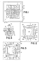
- a chip carrier comprises a ceramic substrate 10, which is generally square in configuration but has one corner 12 cut off as an index marker, and contact pads 14 distributed about the periphery of the upper surface 16 of the substrate.
- the contact pads are the outer ends of conductor runs 15 that extend over the upper surface 16 from inner ends that are distributed about a die pad 18.
- a so-called seal ring 20 of dielectric material bounds a rectangular area of the upper surface of the substrate 10. The inner ends of the conductor runs are within that rectangular area.
- a lead frame 38 having sides 40 bounding a generally rectangular opening has leads 34 extending from each side, like teeth of a comb, into the rectangular opening.
- the center-to-center spacing of the inner ends of the leads 34 is substantially equal to the center-to-center spacing of the contact pads 14 of the chip carrier.
- the lead frame is made of the metal known as Alloy 42.
- the inner ends of the leads are brazed to the contact pads of the chip carrier.
- the lead frame and components electrically connected thereto, for instance the conductor runs 15, are then plated with gold.
- An integrated circuit chip (not shown) is placed on the die pad 18 in a selected orientation relative to the corner 12 of the chip carrier, its contact pads are connected to the inner ends of the conductor runs 15 by wire bonding, and a lid (not shown in FIG. 1) is attached to the top of the seal ring 20 so as to provide an enclosure for the chip.
- the assembly of the chip carrier and the lead frame is placed, with the lid down, on a table (not shown).
- the table has a recess in its upper surface for receiving the lid and the seal ring, so that the lead frame is able to lie flat on the upper surface of the table without being bent.
- the lead frame 38 has holes adjacent two opposite corners. One of these holes is circular and the other hole is somewhat elongated. These two holes fit over pins projecting from the upper surface of the table so as to hold the assembly of the chip carrier and the lead frame against movement relative to the table in directions parallel to the upper surface of the table.
- a lead frame support 30 is fabricated from a sheet of polyimide.
- the lead frame support has four sides 32 surrounding a rectangular opening that is about the same size as the opening surrounded by the four sides 40 of the lead frame.
- Tabs 42 project from the sides 42 respectively of the lead frame support into the opening and are connected to the sides by tongues 46.
- the lead frame support has a layer of adhesive material, such as that sold under the trademark ULTEM, on its lower surface, and is formed with a circular hole and an elongated slot adjacent two opposite corners. The lead frame support is placed over the assembly of the chip carrier and the lead frame so that the pins projecting from the table (and through the holes in the lead frame) pass through the holes in the lead frame support.
- the lead frame support is thereby accurately positioned with respect to the lead frame, with the tabs 42 of the lead frame support above the leads 34 and the sides 32 of the lead frame support above the sides 40 of the lead frame.
- the lower surface of the lead frame support is brought into contact with the upper surface of the lead frame.
- Heat is applied to the adhesive material, and the adhesive material is cured and bonds the support to the lead frame.
- the four sides of the lead frame and the support are removed, by cutting along the dot-dash line 44, leaving the leads 34 electrically isolated from each other and held in position by the tabs 42. Because of the position of the line 44, the outer ends of the leads 34 project beyond the tabs 42.
- the integrated circuit package comprising the ceramic chip carrier 10, the chip itself and the leads 34 attached to the contact pads of the chip carrier is then placed on a lead alignment fixture 50 with the lid down.
- the fixture 50 is a flat plate having pins 52 projecting from its upper surface.
- the pins 52 are positioned for edge contact with the outer ends of the leads 34 and define a unique position for the package on the upper surface of the plate.
- the pins 52 are in predetermined positions relative to a pair of locating posts 54.
- a registration aid is fabricated by punching a generally cruciform blank 62 from a sheet of aluminum.
- the blank has a rectangular portion 64 and arms 66 extending radially from the corners of the rectangular portion.
- the blank is embossed so that the outer ends of the arms are displaced and lie in a common plane that is generally parallel to and spaced from the general plane of the rectangular portion, and holes 68a . . . 68d are formed in the outer ends of the arms.
- the holes 68a, 68c and 68d are each circular, with the holes 68a and 68c somewhat larger than the hole 68d.
- the hole 68b is elongated, in the manner of a slot.
- the direction of elongation is along the line joining the centers of the holes 68b and 68d.
- the width of the hole 68b is the same as the diameter of the hole 68c.
- the centers of the holes 68b, 68c and 68d are at three of the four corners of a square, and the hole 68a is slightly offset from the fourth corner of the square.
- a drop of adhesive material is applied to the top of the package on the alignment fixture 50 (the back surface of the ceramic chip carrier 10), and the registration aid is placed on top of the package with one of the posts 54 in the circular hole 68d and the other post in the slot-form hole 68b.
- the posts 54 are a slip fit in the holes 68b and 68d.
- the holes 68 of the registration aid are thereby located relative to the outer ends of the leads 34 with respect to translation perpendicular to the central axes of the posts 54 and rotation about axes parallel to the central axes of the posts.
- An etched circuit board 70 (FIG. 3) is formed with a rectangular hole 72 which is somewhat larger than the chip carrier 10 but is smaller than the opening defined by the sides of the lead frame.
- the circuit board has conductor runs which terminate in pads 74 which are distributed about the periphery of the rectangular hole 72.
- the circuit board is also formed with circular holes 76 which are in predetermined positions relative to the contact pads 74. The positions of the holes 76 relative to the contact pads 74 correspond to the positions of the holes 68 of the registration aid relative to the outer ends of the leads 34. Threaded posts 78a . . . 78d are fitted in the holes 76 respectively.
- the four posts 78 are identical, and each has five main parts, i.e., a splined cylinder 80 which fits in the hole 76, a flange 82 which engages the upper surface of the circuit board, a cylinder 84 which projects above the upper surface of the circuit board, and threaded parts 86 and 88 which extend respectively above and below the circuit board when the splined cylinder is fitted in the hole 76.
- the cylinders 84 are of uniform height above the upper surface of the flange 82.
- the posts are secured in position by nuts 89 which are fitted on the threaded parts 88 respectively.
- the composite structure of the IC package and registration aid is fitted to the circuit board with the package presented towards the hole 72 in the circuit board and the holes 68 in the arms 66 of the registration aid fitted over the upper cylinders 84 respectively.
- the cylinders 84 are sized for a slip fit in the holes 68b and 68d. Because the hole 68a is offset from the fourth corner of the square defined by the centers of the holes 68b, 68c and 68d, the hole containing the post 78a is similarly offset, and therefore the composite structure has only one possible position relative to the contact pads 74 such that the cylinders 84 each enter one of the holes 68.
- the holes 68a and 68c are sufficiently larger than the cylinders 84 that entry of the cylinders of the pins 78a and 78c in the holes 68a and 68c does not influence the position of the composite structure relative to the circuit board.
- Each side of the frame 90 is formed with a groove 96 at its underside.
- Four bodies 98 of injection molded elastomer material, each of which is T-shaped in cross-section, are bonded to the frame 90 with the bases of the T's in the grooves 96 respectively.
- the clamping frame 90 is fitted to the circuit board so that the posts 78 extend through the holes 94 respectively.
- the leads 34 and the tabs 42 lie between the upper surface of the circuit board and the bodies 98 of elastomer material, and are in registration with respective contact pads 74 of the circuit board.
- Nuts 100 are fitted to the threaded parts 86 of the posts 78, and upon tightening the nuts the frame 90 is clamped to the circuit board and the leads 34 are placed in electrically conductive pressure contact with the contact pads 74 respectively.
- the offset of the outer ends of the arms of the registration aid relative to the central portion thereof is such that the leads 34 and the upper surface of the circuit board are essentially coplanar and therefore the leads 34 provide a short and direct conduction path between the pads 74 of the circuit board and the pads 14 of the chip carrier.
- the upper cylinders 84 of the posts 78 are below the tops of the outer ends of the arms 66 of the registration aid.
- the arms 66, on top of the flanges 82, provide a positive stop with respect to movement of the frame 90 towards the circuit board, and therefore when the nuts 100 are tightened the elastomer material is compressed to a predetermined extent, preferably about 20%, and provides contact force for maintaining the leads 34 in pressure contact with the respective contact pads 74, and the registration aid is firmly clamped to the circuit board.
- a stiffener frame 110 is secured to the underside of the board.
- the stiffener frame is similar to the frame 90 and is fitted over the threaded parts 88 of the posts 78 prior to application of the nuts 89.
- the stiffener frame 110 is particularly suited to cases in which the chip carrier, and consequently the hole in the circuit board, is more than about 2 cm square.
- Heat is conducted from the chip through the substrate to the registration aid, and is transferred by convection from the registration aid to ambient air.
- a convection heat sink 112 may be attached to the registration aid, as also shown in FIG. 5.
- the heat sink is attached to the registration aid using a thermally-conductive adhesive material.
- Ceramic chip carriers are available with their contact pads 14 on the opposite side of the substrate from the chip receiving area.
- the contact pads 14 are connected to conductor runs 102 (FIG. 6) which are on the same side of the carrier as the chip-receiving area by vias 104 formed in the chip carrier.
- the leads can be brought into essentially coplanar relationship with the upper surface of the circuit board without any need for a hole in the circuit board to accommodate the IC package.
- An arrangement of this kind is particularly suited for chips having low power dissipation.
- a multilayer chip carrier is constructed so that all the signal line pads are distributed about the periphery of the upper surface of the ceramic substrate and the ground terminal 110 and the power supply terminals 112 and 114 are on the lower surface of the substrate, as shown in FIG. 7.
- the ground terminal 110 is a ground plane which occupies most of the lower surface of the substrate and the power supply terminals 112 and 114 are pads adjacent opposite respective sides of the lower surface of the substrate.
- a resilient contact frame 116 (FIG. 8) is made from gold-plated beryllium copper and is generally rectangular in form having four sides 118a . . . 118d which bound a generally rectangular opening.
- Leads 120 extend from the sides 118 of the contact frame into the rectangular opening, and are bent at an angle of about 30 degrees out of the plane of the sides 118.
- the circuit board's ground and power supply contact pads 122, 124 and 126 are on the lower surface of the circuit board as shown in FIG. 9 and are provided a light coat of solder creme with flux.
- the contact frame is formed with holes 128 for receiving the threaded parts 88 of the posts 78.
- the contact frame is applied to the bottom surface of the circuit board in a manner such that the leads 120 are directed upwards into the hole in the circuit board and the threaded parts 88 of the posts 78 extend through the holes 128 respectively.
- the stiffener frame 110 is then applied to the posts 78 and is secured in position using the nuts 89.
- the sides 118a and 118b of the contact frame 116 lie under the corresponding sides of the stiffener frame 110, but the contact frame is dimensioned so that the other two sides 118c and 118d are beyond the outer periphery of the stiffener frame.
- the circuit board, with the contact frame and the stiffener frame attached thereto, is subjected to a vapor phase solder operation, and the contact frame is thereby metallurgically bonded to the ground and power supply contact pads. However, the sides 118c and 118d, which lie beyond the outer periphery of the stiffener frame, also lie beyond the power supply contact pads 124 and 126 and therefore are not bonded directly to the circuit board.
- the composite structure of the registration aid and the IC package is presented to the upper surface of the circuit board, in the manner described previously, and the resilience of the leads 120 ensures that there is good electrical contact between the ground and power supply contact pads of the circuit board and the ground and power supply terminals of the substrate.
- the registration aid is attached to the top of the lid of the IC package instead of to the bottom of the substrate.
- a convection heat sink may be attached to the bottom surface of the substrate, as shown in broken lines in FIG. 11. Of course, care must be taken to ensure that the heat sink does not short circuit either of the power supply terminals 112 and 114 to ground.
- the stiffener frame 110 has a bottom plate 140 (FIG. 12) which is formed with an aper ture 142.
- a metal plunger 146 is fitted in the aperture 142, and a compression spring 150 urges the upper end of the plunger into contact with the chip carrier.
- Thermal grease on the upper end of the plunger ensures a good thermally conductive contact between the chip carrier and the plunger 146.
- the plunger is formed with a conduit 152, and cooling water is circulated through this conduit by way of flow and return connections 154, 156 for removing heat from the chip carrier. In this arrangement, the chip carrier can be removed from the circuit board without its being necessary to remove the heat sink components from the circuit board.
- an integrated circuit chip may be mounted in an enclosure comprising a base plate 200 and a wall structure 202 made of dielectric material such as glass or ceramic.
- a metal lead frame 30 is embedded in the wall structure.
- a seal ring 210 is placed on top of the wall structure.
- a substrate 216 having one or more integrated circuit chips 218 mounted thereon is fitted in the enclosure and is bonded to the base plate 200.
- the substrate has contact pads which are connected to the inner ends of the leads 34 by wire bonding.
- the enclosure is sealed by means of a lid 220 which is attached to the seal ring 210.
- the base plate 200 may be made of metal, but in this case only the ground connection is available on the lower surface of the package.
- the wall structure may be made of synthetic polymer material, such as the material known as PPS (polyphenyl sulfide), in which case a seal of epoxy adhesive material might be used instead of the seal ring 210.
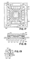
- FIG. 16 illustrates a further modification of the arrangement described with reference to FIGS. 1-12.
- the lead frame 30 includes registration tabs 260 which extend diagonally from the corners of the lead frame and are attached to respective corners of the chip carrier.
- the lead frame is formed with a registration hole 262.
- the holes 262 are in predetermined positions relative to the inner ends of the leads.
- the lead frame support 30 is bonded to the lower side of the lead frame 38, and the lead frame and the support are cut along the dot-dash line 264.
- the leads are thereby separated from the sides 40 of the frame and from the registration tabs 260.
- the leads 34 are bent over out of the plane of the sides of the frame.
- An alignment fixture comprises a flat plate 280 having a group of four posts 282 projecting from its upper surface in a rectangular array, and an additional pair of pins 284.
- a generally rectangular registration aid 286, which also functions as a heat sink, has holes 288a . . . 288d at its four corners.
- the holes 288a, 288c and 288d are circular and the hole 288b is an elongate, slot-form hole.
- the holes 288a and 288c are somewhat larger in diameter than the hole 288d.
- the direction of elongation of the slot-form hole 288b is along the line from the center of that hole to the center of the diagonally-opposite hole 288d.
- the width of the slot-form hole 288b is equal to the diameter of the circular hole 288d.
- the centers of the holes 288b, 288c and 288d are at three of the four corners of a square, and the center of the hole 288a is slightly offset from the fourth corner of the square.
- the registration aid 286 has four bodies 290 of elastomer secured to one surface adjacent the four sides respectively.
- the registration aid is applied to the upper surface of the alignment fixture so that the two pins 284 extend through the holes 288b and 288d respectively.
- the pins are slip fits in the holes, and therefore the registration aid is held against movement relative to the alignment fixture in directions perpendicular to the central axes of the pins.
- the assembly of the chip carrier and the lead frame is fitted to the alignment fixture over the registration aid 286 and the registration holes 262 of the lead frame are fitted over the posts 282 respectively.
- the bent leads then extend over the elastomer bodies 290.
- the circuit board is formed with four holes 296 which receive respective alignment bushings.
- the holes 296 are all the same size, and the relative positions of the holes 296 correspond to the relative positions of the centers of the holes 288.
- Each bushing has a lower portion 298 which is received in the hole of the circuit board and an upper portion 300 which extends above the upper surface of the circuit board.
- the bushings are retained in the holes by soldering to the lower surface of the circuit board.
- the alignment bushings are identical, and the diameter of the upper portions of the bushing is selected so that the upper portions 300 are received with a slip fit in the holes 288b and 288d of the registration aid.
- the composite structure of the registration aid and the package is presented to the upper surface of the circuit board and is fitted so that the upper portions 300 of the bushings enter the holes in the registration aid. There is only one position in which the registration aid can be fitted to the circuit board such that each bushing enters one of the holes of the registration aid.
- the positions of the holes of the circuit board relative to the contact pads that are exposed on the upper surface of the circuit board are predetermined, and correspond to the positions of the holes in the registration aid relative to the outer ends of the leads 34.
- the leads 34 overlie the contact pads of the circuit board.
- Screws 302 are inserted into the bushings and project from the lower ends of the bushes, and enter threaded holes in a heat sink 304 which is positioned beneath the circuit board.
- the base plate of the package may be made of dielectric material, in which case the chip(s) 218 may be mounted directly on the base plate instead of on a separate ceramic substrate.
- the base plate may be provided with an integral heat sink.
- the invention is not restricted to the specific arrangements of chip carrier, seal ring and lid that are illustrated.
- FIG. 13-15 the base plate of the package may be made of dielectric material, in which case the chip(s) 218 may be mounted directly on the base plate instead of on a separate ceramic substrate.
- the base plate may be provided with an integral heat sink.
- FIGS. 8-11 arrangement is not restricted to the terminals on the lower surface of the substrate being ground and power supply terminals.
- the substrate extends beyond the periphery of the lid, and runs 102 extend under the seal ring, so that the vias 104 are located outside the enclosure containing the integrated circuit chip.
Landscapes
- Engineering & Computer Science (AREA)
- Microelectronics & Electronic Packaging (AREA)
- Metallurgy (AREA)
- Manufacturing & Machinery (AREA)
- Manufacturing Of Electrical Connectors (AREA)
- Lead Frames For Integrated Circuits (AREA)
- Facsimile Heads (AREA)
Applications Claiming Priority (2)
| Application Number | Priority Date | Filing Date | Title |
|---|---|---|---|
| US5703 | 1987-01-21 | ||
| US07/005,703 US4758927A (en) | 1987-01-21 | 1987-01-21 | Method of mounting a substrate structure to a circuit board |
Publications (2)
| Publication Number | Publication Date |
|---|---|
| EP0276062A2 true EP0276062A2 (de) | 1988-07-27 |
| EP0276062A3 EP0276062A3 (de) | 1990-01-03 |
Family
ID=21717268
Family Applications (1)
| Application Number | Title | Priority Date | Filing Date |
|---|---|---|---|
| EP88300153A Withdrawn EP0276062A3 (de) | 1987-01-21 | 1988-01-08 | Verfahren zum Montieren eines Bauelementes auf einer Leiterplatte |
Country Status (3)
| Country | Link |
|---|---|
| US (1) | US4758927A (de) |
| EP (1) | EP0276062A3 (de) |
| JP (1) | JPS63198273A (de) |
Cited By (1)
| Publication number | Priority date | Publication date | Assignee | Title |
|---|---|---|---|---|
| GB2276045A (en) * | 1993-02-22 | 1994-09-14 | Yamaichi Electronics Co Ltd | IC Socket |
Families Citing this family (52)
| Publication number | Priority date | Publication date | Assignee | Title |
|---|---|---|---|---|
| US4914812A (en) * | 1987-12-04 | 1990-04-10 | General Electric Company | Method of self-packaging an IC chip |
| JPH04164361A (ja) * | 1990-10-29 | 1992-06-10 | Nec Corp | 樹脂封止型半導体装置 |
| JPH088282B2 (ja) * | 1990-11-28 | 1996-01-29 | インターナシヨナル・ビジネス・マシーンズ・コーポレーシヨン | Tabテープ、半導体チップの結合方法 |
| SE9100597D0 (sv) * | 1991-03-01 | 1991-03-01 | Carlstedt Elektronik Ab | Kapsel foer vlsi-wafer |
| US5136469A (en) * | 1991-07-17 | 1992-08-04 | Stryker Corporation | Powered surgical handpiece incorporating sealed multi semiconductor motor control package |
| US5428504A (en) * | 1992-02-18 | 1995-06-27 | Motorola, Inc. | Cooling cover for RF power devices |
| US5541447A (en) * | 1992-04-22 | 1996-07-30 | Yamaha Corporation | Lead frame |
| JPH0653277A (ja) * | 1992-06-04 | 1994-02-25 | Lsi Logic Corp | 半導体装置アセンブリおよびその組立方法 |
| US5270673A (en) * | 1992-07-24 | 1993-12-14 | Hewlett-Packard Company | Surface mount microcircuit hybrid |
| US5599193A (en) * | 1994-08-23 | 1997-02-04 | Augat Inc. | Resilient electrical interconnect |
| US5949029A (en) * | 1994-08-23 | 1999-09-07 | Thomas & Betts International, Inc. | Conductive elastomers and methods for fabricating the same |
| FR2729045B1 (fr) * | 1994-12-29 | 1997-01-24 | Bull Sa | Procede et dispositif de fixation de deux elements tels qu'un radiateur de circuit integre a une carte de circuits imprimes |
| US5586010A (en) * | 1995-03-13 | 1996-12-17 | Texas Instruments Incorporated | Low stress ball grid array package |
| US5613861A (en) * | 1995-06-07 | 1997-03-25 | Xerox Corporation | Photolithographically patterned spring contact |
| US5672547A (en) * | 1996-01-31 | 1997-09-30 | Industrial Technology Research Institute | Method for bonding a heat sink to a die paddle |
| DE69718693T2 (de) * | 1996-03-08 | 2003-11-27 | Matsushita Electric Industrial Co., Ltd. | Elektronisches Bauteil und Herstellungsverfahren |
| US6175509B1 (en) * | 1997-05-14 | 2001-01-16 | Hewlett-Packard Company | Space efficient local regulator for a microprocessor |
| US6024589A (en) * | 1997-05-14 | 2000-02-15 | Hewlett-Packard Company | Power bus bar for providing a low impedance connection between a first and second printed circuit board |
| US5944537A (en) * | 1997-12-15 | 1999-08-31 | Xerox Corporation | Photolithographically patterned spring contact and apparatus and methods for electrically contacting devices |
| US5979892A (en) * | 1998-05-15 | 1999-11-09 | Xerox Corporation | Controlled cilia for object manipulation |
| JP3864282B2 (ja) * | 1998-09-22 | 2006-12-27 | 三菱マテリアル株式会社 | パワーモジュール用基板及びその製造方法並びにこの基板を用いた半導体装置 |
| US7382142B2 (en) | 2000-05-23 | 2008-06-03 | Nanonexus, Inc. | High density interconnect system having rapid fabrication cycle |
| US6710609B2 (en) * | 2002-07-15 | 2004-03-23 | Nanonexus, Inc. | Mosaic decal probe |
| US7349223B2 (en) | 2000-05-23 | 2008-03-25 | Nanonexus, Inc. | Enhanced compliant probe card systems having improved planarity |
| US6812718B1 (en) | 1999-05-27 | 2004-11-02 | Nanonexus, Inc. | Massively parallel interface for electronic circuits |
| US6799976B1 (en) * | 1999-07-28 | 2004-10-05 | Nanonexus, Inc. | Construction structures and manufacturing processes for integrated circuit wafer probe card assemblies |
| US7247035B2 (en) * | 2000-06-20 | 2007-07-24 | Nanonexus, Inc. | Enhanced stress metal spring contactor |
| US6359334B1 (en) | 1999-06-08 | 2002-03-19 | Micron Technology, Inc. | Thermally conductive adhesive tape for semiconductor devices and method using the same |
| JP3919398B2 (ja) * | 1999-10-27 | 2007-05-23 | 三菱電機株式会社 | 半導体モジュール |
| US6213789B1 (en) | 1999-12-15 | 2001-04-10 | Xerox Corporation | Method and apparatus for interconnecting devices using an adhesive |
| US6570250B1 (en) * | 2000-02-24 | 2003-05-27 | Honeywell International Inc. | Power conditioning substrate stiffener |
| US7579848B2 (en) | 2000-05-23 | 2009-08-25 | Nanonexus, Inc. | High density interconnect system for IC packages and interconnect assemblies |
| US20050068054A1 (en) * | 2000-05-23 | 2005-03-31 | Sammy Mok | Standardized layout patterns and routing structures for integrated circuit wafer probe card assemblies |
| US7952373B2 (en) | 2000-05-23 | 2011-05-31 | Verigy (Singapore) Pte. Ltd. | Construction structures and manufacturing processes for integrated circuit wafer probe card assemblies |
| ATE311604T1 (de) | 2000-06-20 | 2005-12-15 | Nanonexus Inc | Testsystem von integrierten schaltungen |
| US6432291B1 (en) | 2000-08-18 | 2002-08-13 | Advanced Micro Devices, Inc. | Simultaneous electroplating of both sides of a dual-sided substrate |
| US6426290B1 (en) | 2000-08-18 | 2002-07-30 | Advanced Micro Devices, Inc. | Electroplating both sides of a workpiece |
| DE10212721A1 (de) * | 2001-03-24 | 2002-09-26 | Marquardt Gmbh | Ansteuereinrichtung für einen Elektromotor |
| JP2003234442A (ja) * | 2002-02-06 | 2003-08-22 | Hitachi Ltd | 半導体装置及びその製造方法 |
| JP2004200264A (ja) * | 2002-12-17 | 2004-07-15 | Renesas Technology Corp | 半導体装置およびその製造方法 |
| US20080019120A1 (en) * | 2004-01-27 | 2008-01-24 | Carmen Rapisarda | Lighting systems for attachment to wearing apparel |
| JP4536467B2 (ja) * | 2004-09-17 | 2010-09-01 | 株式会社エヌ・ティ・ティ・ドコモ | 平面回路用筐体 |
| US20080079129A1 (en) * | 2006-09-29 | 2008-04-03 | Shankar Ganapathysubramanian | Shape memory based mechanical enabling mechanism |
| US8422243B2 (en) * | 2006-12-13 | 2013-04-16 | Stats Chippac Ltd. | Integrated circuit package system employing a support structure with a recess |
| KR101391925B1 (ko) * | 2007-02-28 | 2014-05-07 | 페어차일드코리아반도체 주식회사 | 반도체 패키지 및 이를 제조하기 위한 반도체 패키지 금형 |
| US8837159B1 (en) | 2009-10-28 | 2014-09-16 | Amazon Technologies, Inc. | Low-profile circuit board assembly |
| US8789965B2 (en) | 2011-11-10 | 2014-07-29 | Carmen Rapisarda | mSolder-less electrical assembly and process for its manufacture |
| US9039442B2 (en) | 2011-11-10 | 2015-05-26 | Carmen Rapisarda | Solder-less electrical assembly |
| CN105659710B (zh) * | 2013-10-30 | 2018-11-09 | 京瓷株式会社 | 布线基板以及使用该布线基板的安装结构体 |
| JP6373115B2 (ja) * | 2014-08-05 | 2018-08-15 | 日本特殊陶業株式会社 | 配線基板 |
| US10333235B1 (en) * | 2018-03-15 | 2019-06-25 | Sten R. Gerfast | Selecting switching functions using screw-force, on modules having traces |
| JP6901603B1 (ja) * | 2020-03-27 | 2021-07-14 | 日本航空電子工業株式会社 | 基板対基板コネクタ |
Family Cites Families (12)
| Publication number | Priority date | Publication date | Assignee | Title |
|---|---|---|---|---|
| US3469684A (en) * | 1967-01-26 | 1969-09-30 | Advalloy Inc | Lead frame package for semiconductor devices and method for making same |
| US3872583A (en) * | 1972-07-10 | 1975-03-25 | Amdahl Corp | LSI chip package and method |
| DE2536711C3 (de) * | 1975-08-18 | 1980-02-28 | Siemens Ag, 1000 Berlin Und 8000 Muenchen | Hochspannungsgleichrichter für Hochspannungskaskaden |
| US4255003A (en) * | 1975-11-13 | 1981-03-10 | Tektronix, Inc. | Electrical connector |
| JPS6028391B2 (ja) * | 1977-10-14 | 1985-07-04 | 株式会社日立製作所 | 半導体パツケージ |
| US4194800A (en) * | 1978-02-21 | 1980-03-25 | Bunker Ramo Corporation | Connector assembly for leadless microcircuit device |
| US4331373A (en) * | 1980-03-24 | 1982-05-25 | Burroughs Corporation | Modular system with system carrier, test carrier and system connector |
| US4390220A (en) * | 1981-04-02 | 1983-06-28 | Burroughs Corporation | Electrical connector assembly for an integrated circuit package |
| US4639829A (en) * | 1984-06-29 | 1987-01-27 | International Business Machines Corporation | Thermal conduction disc-chip cooling enhancement means |
| US4658331A (en) * | 1985-09-09 | 1987-04-14 | Tektronix, Inc. | Mounting an integrated circuit chip to an etched circuit board |
| US4658330A (en) * | 1985-09-09 | 1987-04-14 | Tektronix, Inc. | Mounting a hybrid circuit to a circuit board |
| JPS6267844A (ja) * | 1985-09-20 | 1987-03-27 | Fujitsu Ltd | 冷却構造 |
-
1987
- 1987-01-21 US US07/005,703 patent/US4758927A/en not_active Expired - Lifetime
-
1988
- 1988-01-08 EP EP88300153A patent/EP0276062A3/de not_active Withdrawn
- 1988-01-21 JP JP63011845A patent/JPS63198273A/ja active Granted
Cited By (2)
| Publication number | Priority date | Publication date | Assignee | Title |
|---|---|---|---|---|
| GB2276045A (en) * | 1993-02-22 | 1994-09-14 | Yamaichi Electronics Co Ltd | IC Socket |
| GB2276045B (en) * | 1993-02-22 | 1996-08-28 | Yamaichi Electronics Co Ltd | IC socket |
Also Published As
| Publication number | Publication date |
|---|---|
| JPH0334196B2 (de) | 1991-05-21 |
| EP0276062A3 (de) | 1990-01-03 |
| JPS63198273A (ja) | 1988-08-16 |
| US4758927A (en) | 1988-07-19 |
Similar Documents
| Publication | Publication Date | Title |
|---|---|---|
| EP0276062A2 (de) | Verfahren zum Montieren eines Bauelementes auf einer Leiterplatte | |
| US6320397B1 (en) | Molded plastic carrier for testing semiconductor dice | |
| US5883782A (en) | Apparatus for attaching a heat sink to a PCB mounted semiconductor package | |
| KR100338910B1 (ko) | 전기상호접속어셈블리및이의형성방법 | |
| US9746879B2 (en) | Rigid circuit board with flexibly attached module | |
| US4939570A (en) | High power, pluggable tape automated bonding package | |
| US4652973A (en) | Chip carrier mounting apparatus | |
| US5561594A (en) | Circuit connection in an electrical assembly | |
| US5421079A (en) | High density, high performance memory circuit package | |
| EP0567814B1 (de) | Leiterplatte zur Montage von Halbleitern und sonstigen elektronischen Bauelementen | |
| US5424918A (en) | Universal hybrid mounting system | |
| US4410223A (en) | Module mounting assembly | |
| US6634098B1 (en) | Methods for assembling, modifying and manufacturing a vertical surface mount package | |
| US8899994B2 (en) | Compression connector system | |
| KR970067801A (ko) | 반도체 장치 및 그 제조방법 | |
| US6684493B2 (en) | Vertically mountable interposer, assembly and method | |
| KR100386018B1 (ko) | 스택형반도체디바이스패키지 | |
| US6256202B1 (en) | Integrated circuit intercoupling component with heat sink | |
| EP0216447A2 (de) | Montage eines hybriden Schaltkreises auf einer Leiterplatte | |
| US5062802A (en) | Contact module for a low height multi-chip carrier socket | |
| US5938454A (en) | Electrical connector assembly for connecting first and second circuitized substrates | |
| WO1994028697A1 (en) | Intercoupling component for installing integrated circuit packages on circuit boards | |
| WO1988002980A1 (en) | Interconnection mechanisms for electronic components |
Legal Events
| Date | Code | Title | Description |
|---|---|---|---|
| PUAI | Public reference made under article 153(3) epc to a published international application that has entered the european phase |
Free format text: ORIGINAL CODE: 0009012 |
|
| AK | Designated contracting states |
Kind code of ref document: A2 Designated state(s): DE FR GB NL |
|
| PUAL | Search report despatched |
Free format text: ORIGINAL CODE: 0009013 |
|
| AK | Designated contracting states |
Kind code of ref document: A3 Designated state(s): DE FR GB NL |
|
| 17P | Request for examination filed |
Effective date: 19900502 |
|
| RAP1 | Party data changed (applicant data changed or rights of an application transferred) |
Owner name: TEKTRONIX, INC. |
|
| 17Q | First examination report despatched |
Effective date: 19911211 |
|
| RAP1 | Party data changed (applicant data changed or rights of an application transferred) |
Owner name: TEKTRONIX, INC. |
|
| STAA | Information on the status of an ep patent application or granted ep patent |
Free format text: STATUS: THE APPLICATION IS DEEMED TO BE WITHDRAWN |
|
| 18D | Application deemed to be withdrawn |
Effective date: 19931120 |