EP0269122B2 - Système optique pour laser - Google Patents
Système optique pour laser Download PDFInfo
- Publication number
- EP0269122B2 EP0269122B2 EP87117580A EP87117580A EP0269122B2 EP 0269122 B2 EP0269122 B2 EP 0269122B2 EP 87117580 A EP87117580 A EP 87117580A EP 87117580 A EP87117580 A EP 87117580A EP 0269122 B2 EP0269122 B2 EP 0269122B2
- Authority
- EP
- European Patent Office
- Prior art keywords
- laser
- laser beam
- density distribution
- optical
- distribution filter
- Prior art date
- Legal status (The legal status is an assumption and is not a legal conclusion. Google has not performed a legal analysis and makes no representation as to the accuracy of the status listed.)
- Expired - Lifetime
Links
Images


Classifications
-
- G—PHYSICS
- G02—OPTICS
- G02B—OPTICAL ELEMENTS, SYSTEMS OR APPARATUS
- G02B26/00—Optical devices or arrangements for the control of light using movable or deformable optical elements
- G02B26/08—Optical devices or arrangements for the control of light using movable or deformable optical elements for controlling the direction of light
- G02B26/10—Scanning systems
- G02B26/12—Scanning systems using multifaceted mirrors
- G02B26/127—Adaptive control of the scanning light beam, e.g. using the feedback from one or more detectors
-
- G—PHYSICS
- G02—OPTICS
- G02B—OPTICAL ELEMENTS, SYSTEMS OR APPARATUS
- G02B19/00—Condensers, e.g. light collectors or similar non-imaging optics
- G02B19/0004—Condensers, e.g. light collectors or similar non-imaging optics characterised by the optical means employed
- G02B19/0009—Condensers, e.g. light collectors or similar non-imaging optics characterised by the optical means employed having refractive surfaces only
- G02B19/0014—Condensers, e.g. light collectors or similar non-imaging optics characterised by the optical means employed having refractive surfaces only at least one surface having optical power
-
- G—PHYSICS
- G02—OPTICS
- G02B—OPTICAL ELEMENTS, SYSTEMS OR APPARATUS
- G02B19/00—Condensers, e.g. light collectors or similar non-imaging optics
- G02B19/0033—Condensers, e.g. light collectors or similar non-imaging optics characterised by the use
- G02B19/0047—Condensers, e.g. light collectors or similar non-imaging optics characterised by the use for use with a light source
- G02B19/0052—Condensers, e.g. light collectors or similar non-imaging optics characterised by the use for use with a light source the light source comprising a laser diode
-
- G—PHYSICS
- G02—OPTICS
- G02B—OPTICAL ELEMENTS, SYSTEMS OR APPARATUS
- G02B27/00—Optical systems or apparatus not provided for by any of the groups G02B1/00 - G02B26/00, G02B30/00
- G02B27/09—Beam shaping, e.g. changing the cross-sectional area, not otherwise provided for
-
- G—PHYSICS
- G02—OPTICS
- G02B—OPTICAL ELEMENTS, SYSTEMS OR APPARATUS
- G02B27/00—Optical systems or apparatus not provided for by any of the groups G02B1/00 - G02B26/00, G02B30/00
- G02B27/09—Beam shaping, e.g. changing the cross-sectional area, not otherwise provided for
- G02B27/0927—Systems for changing the beam intensity distribution, e.g. Gaussian to top-hat
-
- G—PHYSICS
- G02—OPTICS
- G02B—OPTICAL ELEMENTS, SYSTEMS OR APPARATUS
- G02B27/00—Optical systems or apparatus not provided for by any of the groups G02B1/00 - G02B26/00, G02B30/00
- G02B27/09—Beam shaping, e.g. changing the cross-sectional area, not otherwise provided for
- G02B27/0938—Using specific optical elements
- G02B27/0988—Diaphragms, spatial filters, masks for removing or filtering a part of the beam
Definitions
- This invention relates to a laser optical system provided with a laser beam source.
- This invention particularly relates to a laser optical system wherein no side lobe is generated to around a convergence spot at the time a laser beam emitted by the laser beam source is converged.
- Laser optical systems have heretofore been widely used as, for example, a means for generating a scanning light beam in scanning recording apparatuses and scanning read-out apparatuses.
- the laser optical system using a semiconductor laser as the laser beam source is advantageous in that the semiconductor laser is smaller, cheaper and consumes less power than a gas laser or the like, and the direct analog modulation wherein the optical output is changed by control of the drive current can be effected, and therefore direct modulation may be carried out by use of signals generated in accordance with image information in the case where the laser optical system is used in a scanning recording apparatus.
- a beam diameter adjusting plate having an aperture through which only the laser beam portion at the center of the laser beam emitted by the laser beam source is to be passed is often disposed in the optical path of the laser beam.
- the beam diameter adjusting plate is used for various purposes, for example for increasing the focal depth at the time the laser beam is converged, as disclosed in Japanese Patent Publication No. 58(1983)-20015.
- the beam diameter adjusting plate is often disposed so that the light in a low output region in the laser beam emitted by the semiconductor laser can also be utilized without increasing the diameter of the convergence spot at the convergence position. The relationship between the output of the semiconductor laser and the diameter of the convergence spot and the effects of the beam diameter adjusting plate will be described hereinbelow.
- Figure 8 shows the relationships between the drive current for the semiconductor laser on one hand and the laser oscillation light and the light in the natural light emission range on the other hand.
- line “a” indicates the relationship between the drive current and the output of the light in the natural light emission region (hereinafter referred to as the natural emission light)
- line “b” indicates the relationship between the drive current and the output of the laser oscillation light.
- the natural emission light contains various angle components as compared with the laser oscillation light, and therefore the natural emission light cannot be converged to a spot diameter so small as the spot diameter of the laser oscillation light. Therefore, in the case where the semiconductor laser optical system is used in a scanning recording apparatus wherein the recording light must be modulated over a wide dynamic range and even a light beam of the low output region in which the natural emission light is predominant must be utilized, the beam diameter in the low output region increases and the spatial resolution of the scanning deteriorates. Accordingly, in Japanese Patent Application No.
- the applicant proposed a semiconductor laser optical system provided with a beam diameter adjusting plate having an aperture through which only the center portion of the laser beam is to be passed on the basis of the findings that the diameter of the convergence spot can be reduced for the natural emission light as well when the beam diameter adjusting plate is disposed in the optical path of the laser beam emitted by the semiconductor laser.
- the beam diameter adjusting plate is used for increasing the focal depth, or, in the case of the semiconductor laser, for preventing the diameter of the convergence spot of the natural emission light from increasing.
- the lens itself may act in the same manner as an aperture and may substantially constitute the beam diameter adjusting member.
- the object of the present invention is to provide a laser optical system wherein only the center portion of the laser beam is taken up and no side lobes are generated when the laser beam portion taken up is converged.
- the present invention achieves its object by providing a laser optical system comprising the features set out in claim 1.
- the density distribution filter may be of an absorption type for absorbing light at a high-density portion, or it may be of a reflection type for reflecting light at the high-density portion.
- the density distribution filter adjusts the passage of the laser beam in accordance with the optical density thereof, there is no risk of a part of the incident laser beam being eclipsed as in the case of the beam diameter adjusting member having an aperture, and no side lobe is generated at the time the laser beam after passage through the density distribution filter is converged.
- the density distribution of the density distribution filter can be selected as desired, and therefore the shape of the laser beam passing through the density distribution filter can easily be adjusted as desired by changing the density distribution of the density distribution filter.
- the beam diameter can be adjusted efficiently by use of the density distribution filter without side lobes being generated. Accordingly, by converging the laser beam passing through the density distribution filter, the focal depth can be increased and blurring of the beam diameter can be eliminated. Thus a good converged laser beam can be obtained at the convergence position.
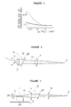
- Figure 1 shows a semiconductor laser optical system in accorance with the present invention.
- the semiconductor laser 1 emits natural emission light and laser oscillation light as mentioned above in accordance with the level of the applied current.
- the laser oscillation light has predetermined intensity distribution in a predetermined radiation angle range, and the intensity in the middle of the radiation angle range becomes the maximum intensity L.
- the laser oscillation light has an elliptical cross-sectional shape wherein the spread angle is different between the longitudinal direction and the transverse direction, and the gradient of a curve 1 differs between the longitudinal direction and the transverse direction.
- the natural emission light contains various angle components and is radiated also in directions different from the directions of radiation of the laser oscillation light.
- a current is applied to a semiconductor laser 1, and the semiconductor laser 1 emits a laser beam 1A in a light emission amount in accordance with the level of the current.
- the laser beam 1A generated by the semiconductor laser 1 is collimated by a collimator lens 2 disposed in the optical path, and then impinges upon a density distribution filter 23 which is constituted so that the optical density at the center portion is lower and the optical density at the peripheral portion is higher, and only the low density portion substantially transmits light.
- the density distribution filter 23 is used for decreasing the diameter of the convergence spot of the laser beam in the low output region, wherein the natural emission light is predominant, to a value close to the diameter of the convergence spot of the laser oscillation light.
- the diameter of the convergence spot of the laser beam in the low output region can be made smaller as the size of the low density portion is made smaller to decrease the diameter of the laser beam passing through the low density portion.
- the density distribution filter 23 is constituted as shown in Figure 3A so that a rectangular low density portion 23a is formed inward from a high density portion 23b, which substantially intercepts light.
- the optical transmittance of the density distribution filter 23 in the transverse direction (i.e. in the x direction) and the optical transmittance thereof in the longitudinal direction i.e.
- the sizes of the low density portion 23a in the x direction and in the y direction are smaller than the beam diameter of the laser oscillation light.
- the low density portion 23a may have any shape insofar as the longitudinal and transverse widths are suitable for taking up the laser beam of a desirable diameter.
- the shape of the low density portion 23a may be elliptical as shown in Figure 3B.
- the optical transmittance of the density distribution filter 23 in the x direction and the optical transmittance thereof in the y direction become as shown in Figure 3B.
- the density distribution of the density distribution filter 23 need not be such that the low density portion and the high density portion are continuously changed gradually as mentioned above, and may be such that the density decreases stepwise toward the center of the filter.
- the maximum value Tmax and the minimum value Tmin of the transmittance of the density distribution filter 23 should preferably be different from each other by at least one order of ten.
- the density distribution of the filter need not be formed in two-dimensional directions, and may be formed only in a one-dimensional direction in the case where problems with regard to increase in the diameter of the convergence spot of the natural emission light and the like are allowable in one direction.
- the laser beam 1A' passing through the density distribution filter 23 is converged by the converging lens 4 to a predetermined convergence position Q.
- the density distribution filter 23 is not disposed in the optical path of the laser beam 1A emitted by the semiconductor laser 1
- the relationship between the output of the semiconductor laser 1 and the diameter of the convergence spot becomes as indicated by the broken line in Figure 5.
- the diameter of the convergence spot relative to the diameter of the convergence spot at the time of the output of 3mW wherein substantially the laser oscillation light alone is generated is taken as 1.
- the diameter of the convergence spot of the laser beam in the low output region wherein only the natural emission light is generated or the natural emission light is predominant becomes very large.
- the diameter of the convergence spot of the laser beam in the low output region can be reduced by the effects of the density distribution filter 23.
- each of the longitudinal width W and the transverse width W of the portion of the density distribution filter 23 corresponding to the transmittance range from the maximum value Tmax to one-half of the maximum value Tmax, i.e. Tmax/2. in the optical transmittance distribution as shown in Figure 11 is.
- the diameter of the convergence spot can be made markedly smaller than in the conventional laser optical system in the low output region as well. Also. no side lobe is generated at the convergence position, and the converged beam constituted by the zero-order light component alone can be obtained.
- the density distribution filter 23 is disposed between the collimator lens 2 and the converging lens 4, the density distribution filter 23 may be disposed at any position in the optical path between the semiconductor laser 1 and the convergence position Q. Also, the density distribution filter 23 may be incorporated inside of the collimator lens or inside of the converging lens 4. The size of the low density portion of the density distribution filter 23 may be adjusted to a value suitable for the beam diameter of the incident laser beam in accordance with the location of the density distribution filter 23.
- the density distribution filter 23 is positioned normal to the optical axis of the incident laser beam 1A as shown in Figure 1, it may occur that a part of tne laser beam 1A reflected by the surface of the density distribution filter 23 passes through the collimator lens 2 and returns to the semiconductor laser 1.
- the reflected laser beam is returned to the semiconductor laser 1 in this manner, mode hopping occurs or the output of the semiconductor laser 1 is caused to fluctuate by optical interference.
- the adverse effects of returning of the reflected laser beam returning also arise in the cases of lasers other than the semiconductor laser.
- a density distribution filter 23 may be positioned obliquely with respect to the optical axis of the laser beam 1A emitted by the semiconductor laser 1.
- the optical path of a laser beam 1B reflected by the density distribution filter 23' is shifted upward obliquely, so that no laser beam is returned to the semiconductor laser 1 and the aforesaid problems can be avoided.
- the density distribution (reflectivity distribution) of the density distribution filter 23' may be adjusted to an appropriate condition in accordance with the angle of inclination of the density distribution filter 23'.
- a semiconductor laser chip 1' supported by a supporting base 26 is disposed so that a laser beam 1C emitted from the back of the semiconductor laser chip 1' is detected by the photodetector 25.
- the photodetector 25 controls the drive current for the semiconductor laser chip 1' in accordance with the output of the laser beam 1C, so that the optical amount of the laser beam 1A emitted forward by the semiconductor laser chip 1' is always kept constant.
- the density distribution filter 23' is inclined as shown to eliminate interference of the reflected laser beam 1B with the laser beam 1C and to carry out the automatic control of the laser power accurately.
- a laser beam 11A emitted by a semiconductor laser 11 is collimated by a collimator lens 12, and is then made to impinge upon a density distribution filter 33.
- the density distribution filter 33 is of the light absorbing type, and is therefore disposed normal to the optical axis of the laser beam 11A.
- the laser beam 11A has a horizontally long elliptical beam shape as indicated by the broken line in Figure 9, and a low density portion 33a formed inward from a high density portion 33b of the density distribution filter 33 is provided to restrict the passage of the laser beam 11A therethrough only in the shorter axis direction (i.e. in the vertical direction in Figure 9.
- laser beam 11A' passing through the density distribution filter 33 has its beam shape contracted vertically as compared with the beam shape of the laser beam 11A.
- the laser beam 11A' passing through the density distribution filter 33 is converged by a cylindrical lens 17, which is disposed in the optical path, only in the vertical direction.
- the laser beam 11A' is thus made to impinge upon a rotating polygon mirror 18, which is rotating in the direction as indicated by the arrow A, as a linear image normal to the drive axis of the rotating polygon mirror 18.
- the rotating polygon mirror 18 reflects and deflects the laser beam 11A' in a main scanning direction, and the deflected laser beam 11A' is passed through an f ⁇ lens 19 constituted by a combination of two lenses.
- the deflected laser beam 11A' is then passed through a cylindrical mirror 20 disposed in the optical path to extend in the main scanning direction, and repeatedly scans a surface 21, which is to be scanned and is being conveyed in a sub-scanning direction as indicated by the arrow B. in the main scanning direction indicated by the arrow A'.
- the cylindrical mirror 20 converges the incident laser beam 11A' only in the sub-scanning direction on the surface 21 which is to be scanned, and the distance between the f ⁇ lens 19 and the surface 21 which is to be scanned is adjusted to be equal to the focal length of the f ⁇ lens 19 as a whole.
- the cylindrical lens 17 and the cylindrical mirror 20 are disposed, and the laser beam 11A' is converged onto the rotating polygon mirror 18 only in the sub-scanning direction. Therefore, even though surface inclination or axis deviation arises with the rotating polygon mirror 18, the scanning position of the laser beam 11A' on the surface 21 which is to be scanned does not deviate in the sub-scanning direction, and scanning lines free of splits in the sub-scanning direction can be formed at equal intervals. Also, in such an optical scanning apparatus, high accuracy of the diameter of the convergence spot on the surface 21 which is to be scanned is required, particularly in the sub-scanning direction.
- the diameter of the convergence spot is adjusted in the vertical direction, which corresponds to the sub-scanning direction, by the density distribution filter 33 in the optical path prior to the impingement of the laser beam 11A' upon the rotating polygon mirror 18 as mentioned above, the therefore the problem with regard to beam blur in the sub-scanning direction on the surface 21 which is to be scanned does not arise.
- the adjustment of the diameter of the convergence spot is carried out by the density distribution filter 33, and the laser beam 11A is not completely eclipsed in the course of the adjustment. Therefore, no side lobe is generated on the surface 21 which is to be scanned and on which the laser beam 11A' is converged. Accordingly, scanning can be carried out accurately on the surface 21 which is to be scanned so that no beam diameter blur appears in the sub-scanning direction and no side lobe is generated.
- the laser optical system in accordance with the present invention is described above as an example.
- the desirable density distribution of the density distribution filter varies in accordance with the purpose of the adjustment of the beam diameter.
- the diameter of the collimator lens is adjusted to be smaller than, for example, the diameter of the incident laser beam
- the collimator lens as a whole acts in the same manner as an aperture, and a part of the laser beam is eclipsed by the collimator lens.
- the density distribution filter can achieve the effects of cutting off the eclipsed laser beam and preventing the generation of side lobes as well as the original purposes of the density distribution filter.
Landscapes
- Physics & Mathematics (AREA)
- General Physics & Mathematics (AREA)
- Optics & Photonics (AREA)
- Mechanical Optical Scanning Systems (AREA)
Claims (3)
- Système optique pour laser comprenant :un laser à semiconducteur (1) du type modulation analogique directe :un moyen de pilotage conçu pour piloter le laser à semiconducteur (1) dans les deux plages de l'émission de lumière naturelle et de l'émission de lumière laser ;une lentille de convergence (4) servant à faire converger un faisceau laser émis par ledit laser en une position de convergence prédéterminée (Q) ; etun filtre de distribution de densité (23) disposé dans un chemin optique dudit faisceau laser à l'avant de ladite lentille de convergence, constitué de telle sorte que la densité optique au niveau de la partie centrale (23a) soit inférieure et que la densité optique au niveau de la partie périphérique (23b) soit supérieure, si bien que seule la partie à faible densité transmet significativement le faisceau lumineux ; la partie haute densité arrête significativement le faisceau de lumière de façon que le spot (ou tache) de convergence du faisceau laser soit empêché d'augmenter lorsque le faisceau laser est piloté dans la région de l'émission de lumière naturelle ; et la transmittance décroít progressivement depuis sa partie centrale jusqu'à sa partie périphérique.
- Système optique pour laser selon la revendication 1, dans lequel ledit filtre de distribution de densité est incliné d'un angle prédéterminé par rapport au chemin optique dudit faisceau laser.
- Système optique pour laser selon la revendication 1, dans lequel ledit filtre de distribution de densité est formé de telle sorte que la valeur maximum Tmax et que la valeur minimum Tmin de la transmittance optique soient différentes l'une de l'autre d'au moins un ordre de dix.
Applications Claiming Priority (9)
| Application Number | Priority Date | Filing Date | Title |
|---|---|---|---|
| JP28364886 | 1986-11-28 | ||
| JP28364786 | 1986-11-28 | ||
| JP283648/86 | 1986-11-28 | ||
| JP28364886 | 1986-11-28 | ||
| JP283647/86 | 1986-11-28 | ||
| JP61283647A JPH0727129B2 (ja) | 1986-11-28 | 1986-11-28 | レ−ザ光学系 |
| JP197734/87 | 1987-08-07 | ||
| JP62197734A JP2623093B2 (ja) | 1986-11-28 | 1987-08-07 | レーザ光学系 |
| JP19773487 | 1987-08-07 |
Publications (4)
| Publication Number | Publication Date |
|---|---|
| EP0269122A2 EP0269122A2 (fr) | 1988-06-01 |
| EP0269122A3 EP0269122A3 (en) | 1989-05-24 |
| EP0269122B1 EP0269122B1 (fr) | 1994-10-26 |
| EP0269122B2 true EP0269122B2 (fr) | 1999-08-11 |
Family
ID=27327404
Family Applications (1)
| Application Number | Title | Priority Date | Filing Date |
|---|---|---|---|
| EP87117580A Expired - Lifetime EP0269122B2 (fr) | 1986-11-28 | 1987-11-27 | Système optique pour laser |
Country Status (3)
| Country | Link |
|---|---|
| US (1) | US4832446A (fr) |
| EP (1) | EP0269122B2 (fr) |
| DE (1) | DE3750693T3 (fr) |
Families Citing this family (32)
| Publication number | Priority date | Publication date | Assignee | Title |
|---|---|---|---|---|
| US4963003A (en) * | 1988-02-22 | 1990-10-16 | Fuji Photo Film Co., Ltd. | Laser optical system |
| DE3833727A1 (de) * | 1988-10-04 | 1990-04-05 | Sick Optik Elektronik Erwin | Optische abtastvorrichtung |
| US4982206A (en) * | 1989-01-03 | 1991-01-01 | Eastman Kodak Company | Laser printer having an apodizine mask |
| US5116110A (en) * | 1989-03-03 | 1992-05-26 | Greyhawk Systems, Inc. | Partially coherent optical system with scattering type object |
| KR920704159A (ko) * | 1989-08-21 | 1992-12-19 | 알. 아모스 칼 | 전자현상 조작방법 및 장치 |
| US5111343A (en) * | 1990-05-29 | 1992-05-05 | Eastman Kodak Company | Gradient filter |
| US5048938A (en) * | 1990-06-08 | 1991-09-17 | United Technologies Corporation | Monolithic laser spatial filter |
| US5274491A (en) * | 1991-05-13 | 1993-12-28 | Ncr Corporation | Dynamic laser diode aperture for optical scanners |
| JPH06148573A (ja) * | 1992-11-09 | 1994-05-27 | Olympus Optical Co Ltd | 瞳変調光学系 |
| FR2715480B1 (fr) * | 1994-01-21 | 1996-03-08 | Georges Gaillard | Procédé et dispositif de répartition spatiale de l'énergie d'un faisceau de rayonnement cohérent. |
| JP3531199B2 (ja) * | 1994-02-22 | 2004-05-24 | 三菱電機株式会社 | 光伝送装置 |
| JPH07234382A (ja) * | 1994-02-24 | 1995-09-05 | Matsushita Electric Ind Co Ltd | 超解像走査光学装置 |
| US5768017A (en) * | 1994-10-31 | 1998-06-16 | International Business Machines Corporation | Optical system for producing uniform line illumination |
| JP3369101B2 (ja) | 1998-03-11 | 2003-01-20 | 富士写真フイルム株式会社 | レーザ記録装置 |
| US6154326A (en) * | 1998-03-19 | 2000-11-28 | Fuji Xerox Co., Ltd. | Optical head, disk apparatus, method for manufacturing optical head, and optical element |
| DE19816040A1 (de) * | 1998-04-09 | 1999-10-14 | Heidelberger Druckmasch Ag | Verlaufsblende für Belichtungsgeräte |
| US6542304B2 (en) | 1999-05-17 | 2003-04-01 | Toolz, Ltd. | Laser beam device with apertured reflective element |
| US7291805B2 (en) * | 2003-10-30 | 2007-11-06 | The Regents Of The University Of California | Target isolation system, high power laser and laser peening method and system using same |
| US7199330B2 (en) * | 2004-01-20 | 2007-04-03 | Coherent, Inc. | Systems and methods for forming a laser beam having a flat top |
| JP4847201B2 (ja) * | 2006-04-27 | 2011-12-28 | 株式会社リコー | 光源システム、光走査装置、画像形成装置、光量制御方法、光走査方法、及び画像形成方法 |
| US7545838B2 (en) * | 2006-06-12 | 2009-06-09 | Coherent, Inc. | Incoherent combination of laser beams |
| JP5042580B2 (ja) | 2006-09-29 | 2012-10-03 | 富士フイルム株式会社 | 半導体レーザ光源ユニット |
| US20080151951A1 (en) * | 2006-12-22 | 2008-06-26 | Elliott David J | Laser optical system |
| US20090323739A1 (en) * | 2006-12-22 | 2009-12-31 | Uv Tech Systems | Laser optical system |
| EP1942500B1 (fr) * | 2007-01-08 | 2010-06-30 | Samsung Electronics Co., Ltd. | Capture optique incluant unité pour éliminer la diaphonie dans un disque multicouche et appareil d'enregistrement optique et/ou de reproduction incluant la capture optique |
| EP2284436B1 (fr) | 2009-08-05 | 2012-02-08 | Kai Stapelfeldt | Dispositif de production d'un rayon lumineux essentiellement linéaire ayant un élargissement latéral réduit |
| CN102928982B (zh) * | 2011-08-10 | 2017-04-05 | 上海雄博精密仪器股份有限公司 | 一种大口径平行光扩束装置及方法 |
| EP2969368A4 (fr) * | 2013-03-12 | 2016-11-16 | Applied Materials Inc | Forme personnalisée de diaphragme à pupille pour la maîtrise du profil de contour dans les systèmes de recuit par laser |
| JP6233192B2 (ja) * | 2014-05-29 | 2017-11-22 | 京セラドキュメントソリューションズ株式会社 | 光走査装置、画像形成装置 |
| JP6193305B2 (ja) * | 2014-07-29 | 2017-09-06 | ウルトラテック インク | 高性能線形成光学システム及び方法 |
| US9613815B2 (en) * | 2014-11-24 | 2017-04-04 | Ultratech, Inc. | High-efficiency line-forming optical systems and methods for defect annealing and dopant activation |
| SG10201605683WA (en) * | 2015-07-22 | 2017-02-27 | Ultratech Inc | High-efficiency line-forming optical systems and methods using a serrated spatial filter |
Family Cites Families (9)
| Publication number | Priority date | Publication date | Assignee | Title |
|---|---|---|---|---|
| US3900884A (en) * | 1969-12-11 | 1975-08-19 | Holotron Corp | Holographic color television record system |
| US3868637A (en) * | 1971-09-30 | 1975-02-25 | Michael S Schiller | Document retrieval system |
| US4088964A (en) * | 1975-01-22 | 1978-05-09 | Clow Richard G | Multi-mode threshold laser |
| US4089589A (en) * | 1976-05-11 | 1978-05-16 | Iowa State University Research Foundation, Inc. | Optical signal processing system and method |
| US4158176A (en) * | 1977-09-06 | 1979-06-12 | The United States Of America As Represented By The United States Department Of Energy | Spatial filter system as an optical relay line |
| US4304467A (en) * | 1979-05-29 | 1981-12-08 | International Business Machines Corporation | Focussed laser beam optical system |
| US4464021A (en) * | 1981-04-01 | 1984-08-07 | United Technologies Corporation | Isolator for high power radiation |
| CA1208466A (fr) * | 1982-07-28 | 1986-07-29 | Donald R. Scifres | Collimation et focalisation des faisceaux de lasers a plusieurs emetteurs ou a emetteur large |
| US4656641A (en) * | 1985-02-04 | 1987-04-07 | Xerox Corporation | Laser cavity optical system for stabilizing the beam from a phase locked multi-emitter broad emitter laser |
-
1987
- 1987-11-27 EP EP87117580A patent/EP0269122B2/fr not_active Expired - Lifetime
- 1987-11-27 US US07/127,018 patent/US4832446A/en not_active Expired - Lifetime
- 1987-11-27 DE DE3750693T patent/DE3750693T3/de not_active Expired - Lifetime
Also Published As
| Publication number | Publication date |
|---|---|
| EP0269122B1 (fr) | 1994-10-26 |
| DE3750693D1 (de) | 1994-12-01 |
| EP0269122A3 (en) | 1989-05-24 |
| US4832446A (en) | 1989-05-23 |
| EP0269122A2 (fr) | 1988-06-01 |
| DE3750693T3 (de) | 1999-12-23 |
| DE3750693T2 (de) | 1995-02-23 |
Similar Documents
| Publication | Publication Date | Title |
|---|---|---|
| EP0269122B2 (fr) | Système optique pour laser | |
| US4656641A (en) | Laser cavity optical system for stabilizing the beam from a phase locked multi-emitter broad emitter laser | |
| US6704129B2 (en) | Optical scanning apparatus capable of reducing variations in shading and improving light usage | |
| US5257125A (en) | Afocal optical system for focus error correction in laser scanning systems | |
| EP0132956A2 (fr) | Appareil de balayage par rayons lumineux | |
| JP2002040350A (ja) | 光走査装置 | |
| US4993792A (en) | Scanning optical system in which a ghost image is eliminated | |
| US4998790A (en) | Optical scanning apparatus | |
| EP0100242A2 (fr) | Système optique pour un laser | |
| US5161047A (en) | Optical scanner for image recording apparatus | |
| JP2623093B2 (ja) | レーザ光学系 | |
| JP3627453B2 (ja) | 光学走査装置 | |
| US4797894A (en) | Alignment method and arrangement for external optical feedback for semiconductor diode lasers | |
| JPH0695018A (ja) | ラスター出力スキャナー | |
| US4806753A (en) | Light scanning device with a short-path synchronizing grid | |
| JPS63136018A (ja) | レ−ザ光学系 | |
| US5276544A (en) | Two element optical system for focus error correction in laser scanning systems | |
| JP3073790B2 (ja) | 光走査装置 | |
| JP3681120B2 (ja) | マルチビーム走査装置、光源装置 | |
| EP0176329A2 (fr) | Diodes laser | |
| US6785305B1 (en) | Tuneable, adjustment-stable semiconductor laser light source and a method for the optically stable, largely continuous tuning of semiconductor lasers | |
| US4807992A (en) | Method of detecting semiconductor laser mode hopping and semiconductor laser beam source apparatus | |
| US5191463A (en) | Scanning optical system in which a ghost image is elminated | |
| JPH0588100A (ja) | 走査装置 | |
| JP2767618B2 (ja) | レーザー走査光学装置 |
Legal Events
| Date | Code | Title | Description |
|---|---|---|---|
| PUAI | Public reference made under article 153(3) epc to a published international application that has entered the european phase |
Free format text: ORIGINAL CODE: 0009012 |
|
| AK | Designated contracting states |
Kind code of ref document: A2 Designated state(s): DE FR NL |
|
| PUAL | Search report despatched |
Free format text: ORIGINAL CODE: 0009013 |
|
| AK | Designated contracting states |
Kind code of ref document: A3 Designated state(s): DE FR NL |
|
| 17P | Request for examination filed |
Effective date: 19890714 |
|
| 17Q | First examination report despatched |
Effective date: 19910805 |
|
| GRAA | (expected) grant |
Free format text: ORIGINAL CODE: 0009210 |
|
| AK | Designated contracting states |
Kind code of ref document: B1 Designated state(s): DE FR NL |
|
| REF | Corresponds to: |
Ref document number: 3750693 Country of ref document: DE Date of ref document: 19941201 |
|
| ET | Fr: translation filed | ||
| PLBI | Opposition filed |
Free format text: ORIGINAL CODE: 0009260 |
|
| 26 | Opposition filed |
Opponent name: ASAHI KOGAKU KOGYO KK Effective date: 19950725 |
|
| NLR1 | Nl: opposition has been filed with the epo |
Opponent name: ASAHI KOGAKU KOGYO KK |
|
| PLBF | Reply of patent proprietor to notice(s) of opposition |
Free format text: ORIGINAL CODE: EPIDOS OBSO |
|
| PLBF | Reply of patent proprietor to notice(s) of opposition |
Free format text: ORIGINAL CODE: EPIDOS OBSO |
|
| RDAH | Patent revoked |
Free format text: ORIGINAL CODE: EPIDOS REVO |
|
| APAC | Appeal dossier modified |
Free format text: ORIGINAL CODE: EPIDOS NOAPO |
|
| APAE | Appeal reference modified |
Free format text: ORIGINAL CODE: EPIDOS REFNO |
|
| APAC | Appeal dossier modified |
Free format text: ORIGINAL CODE: EPIDOS NOAPO |
|
| APAC | Appeal dossier modified |
Free format text: ORIGINAL CODE: EPIDOS NOAPO |
|
| PLAW | Interlocutory decision in opposition |
Free format text: ORIGINAL CODE: EPIDOS IDOP |
|
| PLAW | Interlocutory decision in opposition |
Free format text: ORIGINAL CODE: EPIDOS IDOP |
|
| PUAH | Patent maintained in amended form |
Free format text: ORIGINAL CODE: 0009272 |
|
| STAA | Information on the status of an ep patent application or granted ep patent |
Free format text: STATUS: PATENT MAINTAINED AS AMENDED |
|
| 27A | Patent maintained in amended form |
Effective date: 19990811 |
|
| AK | Designated contracting states |
Kind code of ref document: B2 Designated state(s): DE FR NL |
|
| ET3 | Fr: translation filed ** decision concerning opposition | ||
| NLR3 | Nl: receipt of modified translations in the netherlands language after an opposition procedure | ||
| APAH | Appeal reference modified |
Free format text: ORIGINAL CODE: EPIDOSCREFNO |
|
| PGFP | Annual fee paid to national office [announced via postgrant information from national office to epo] |
Ref country code: FR Payment date: 20061117 Year of fee payment: 20 |
|
| PGFP | Annual fee paid to national office [announced via postgrant information from national office to epo] |
Ref country code: NL Payment date: 20061121 Year of fee payment: 20 |
|
| PGFP | Annual fee paid to national office [announced via postgrant information from national office to epo] |
Ref country code: DE Payment date: 20070102 Year of fee payment: 20 |
|
| REG | Reference to a national code |
Ref country code: FR Ref legal event code: TP Ref country code: FR Ref legal event code: CD |
|
| PG25 | Lapsed in a contracting state [announced via postgrant information from national office to epo] |
Ref country code: NL Free format text: LAPSE BECAUSE OF EXPIRATION OF PROTECTION Effective date: 20071127 |
|
| NLV7 | Nl: ceased due to reaching the maximum lifetime of a patent |
Effective date: 20071127 |
|
| PLAB | Opposition data, opponent's data or that of the opponent's representative modified |
Free format text: ORIGINAL CODE: 0009299OPPO |