EP0268523A1 - Optische Einkopplungsvorrichtung für optischen Direktverstärker - Google Patents
Optische Einkopplungsvorrichtung für optischen Direktverstärker Download PDFInfo
- Publication number
- EP0268523A1 EP0268523A1 EP87402475A EP87402475A EP0268523A1 EP 0268523 A1 EP0268523 A1 EP 0268523A1 EP 87402475 A EP87402475 A EP 87402475A EP 87402475 A EP87402475 A EP 87402475A EP 0268523 A1 EP0268523 A1 EP 0268523A1
- Authority
- EP
- European Patent Office
- Prior art keywords
- wavelength
- optical
- polarization
- optical fiber
- polarization prism
- Prior art date
- Legal status (The legal status is an assumption and is not a legal conclusion. Google has not performed a legal analysis and makes no representation as to the accuracy of the status listed.)
- Granted
Links
- 230000003287 optical effect Effects 0.000 title claims abstract description 49
- 230000010287 polarization Effects 0.000 claims abstract description 54
- 239000013307 optical fiber Substances 0.000 claims abstract description 50
- 239000004065 semiconductor Substances 0.000 claims abstract description 20
- 238000001069 Raman spectroscopy Methods 0.000 claims abstract description 18
- 230000005540 biological transmission Effects 0.000 claims abstract description 17
- 230000000694 effects Effects 0.000 claims abstract description 17
- 230000003321 amplification Effects 0.000 claims abstract description 4
- 238000003199 nucleic acid amplification method Methods 0.000 claims abstract description 4
- 230000009021 linear effect Effects 0.000 claims description 8
- VYPSYNLAJGMNEJ-UHFFFAOYSA-N Silicium dioxide Chemical compound O=[Si]=O VYPSYNLAJGMNEJ-UHFFFAOYSA-N 0.000 description 4
- 230000008901 benefit Effects 0.000 description 4
- 239000007787 solid Substances 0.000 description 4
- 230000008878 coupling Effects 0.000 description 3
- 238000010168 coupling process Methods 0.000 description 3
- 238000005859 coupling reaction Methods 0.000 description 3
- 239000000463 material Substances 0.000 description 3
- 239000004821 Contact adhesive Substances 0.000 description 2
- 230000004048 modification Effects 0.000 description 2
- 238000012986 modification Methods 0.000 description 2
- 239000000377 silicon dioxide Substances 0.000 description 2
- 101150087426 Gnal gene Proteins 0.000 description 1
- 238000004891 communication Methods 0.000 description 1
- 238000000034 method Methods 0.000 description 1
- 230000009022 nonlinear effect Effects 0.000 description 1
- 230000008569 process Effects 0.000 description 1
- 230000007704 transition Effects 0.000 description 1
Images


Classifications
-
- G—PHYSICS
- G02—OPTICS
- G02B—OPTICAL ELEMENTS, SYSTEMS OR APPARATUS
- G02B6/00—Light guides; Structural details of arrangements comprising light guides and other optical elements, e.g. couplings
- G02B6/24—Coupling light guides
- G02B6/42—Coupling light guides with opto-electronic elements
- G02B6/4201—Packages, e.g. shape, construction, internal or external details
- G02B6/4246—Bidirectionally operating package structures
-
- G—PHYSICS
- G02—OPTICS
- G02B—OPTICAL ELEMENTS, SYSTEMS OR APPARATUS
- G02B6/00—Light guides; Structural details of arrangements comprising light guides and other optical elements, e.g. couplings
- G02B6/24—Coupling light guides
- G02B6/26—Optical coupling means
- G02B6/28—Optical coupling means having data bus means, i.e. plural waveguides interconnected and providing an inherently bidirectional system by mixing and splitting signals
- G02B6/293—Optical coupling means having data bus means, i.e. plural waveguides interconnected and providing an inherently bidirectional system by mixing and splitting signals with wavelength selective means
- G02B6/29346—Optical coupling means having data bus means, i.e. plural waveguides interconnected and providing an inherently bidirectional system by mixing and splitting signals with wavelength selective means operating by wave or beam interference
- G02B6/29361—Interference filters, e.g. multilayer coatings, thin film filters, dichroic splitters or mirrors based on multilayers, WDM filters
- G02B6/29362—Serial cascade of filters or filtering operations, e.g. for a large number of channels
- G02B6/29365—Serial cascade of filters or filtering operations, e.g. for a large number of channels in a multireflection configuration, i.e. beam following a zigzag path between filters or filtering operations
- G02B6/29367—Zigzag path within a transparent optical block, e.g. filter deposited on an etalon, glass plate, wedge acting as a stable spacer
-
- H—ELECTRICITY
- H01—ELECTRIC ELEMENTS
- H01S—DEVICES USING THE PROCESS OF LIGHT AMPLIFICATION BY STIMULATED EMISSION OF RADIATION [LASER] TO AMPLIFY OR GENERATE LIGHT; DEVICES USING STIMULATED EMISSION OF ELECTROMAGNETIC RADIATION IN WAVE RANGES OTHER THAN OPTICAL
- H01S3/00—Lasers, i.e. devices using stimulated emission of electromagnetic radiation in the infrared, visible or ultraviolet wave range
- H01S3/30—Lasers, i.e. devices using stimulated emission of electromagnetic radiation in the infrared, visible or ultraviolet wave range using scattering effects, e.g. stimulated Brillouin or Raman effects
- H01S3/302—Lasers, i.e. devices using stimulated emission of electromagnetic radiation in the infrared, visible or ultraviolet wave range using scattering effects, e.g. stimulated Brillouin or Raman effects in an optical fibre
Definitions
- the present invention relates to an optical coupler, which is used as an optical source of an optical direct amplifier using the stimulated Raman scatter effect in an optical fiber.
- the Raman effect is the phenomenon that when light of the angle frequency ( ⁇ ) illuminates a material, another light of the angle frequency ( ⁇ ) is generated depending upon the transition of the transmition of the vibration state and/or the spin state of the material.
- the light of ( ⁇ - ⁇ ) is called stokes light, and the light of ( ⁇ + ⁇ ) is called anti-stokes light.
- An optical direct amplification is carried out by using the stimulated Raman scatter phenomenon by non-linear effect of an optical fiber.
- an amplifier is reported in No.1115, 4-239 and No.1113, 4-237 in the annual meeting in 1985 of the Institute of Electronics and Communication in Japan.
- Fig.7 shows a prior optical direct amplifier using stimulated Raman scatter effect.
- the numeral 71 is a pump light source
- 72 is a light combiner (multiplexer)
- 73 is a wavelength separator
- 74 is an optical fiber for pump light
- 75 is an optical fiber for signal
- 76 is an optical fiber for transmission (Raman effect).
- the pump light in the optical fiber 74 is combined with the signal light in the optical fiber 75. Then, the combined light is transmitted in the optical fiber 76, where the signal light is amplified by the stimulated Raman effect.
- the wavelength separator 73 separates only the desired wavelength as an amplified output signal.
- the pump wavelength is selected so that the stokes wavelength generated by the pump wavelength is almost the same as the wavelength of the signal to be amplified. Therefore, a high power pump light source 71 and an optical coupler 72 for coupling both pump light and signal light to a common optical fiber are essential.
- a pump light source 71 is a solid laser like a YAG laser.
- an optical combiner 72 for combining a pump light with a signal light is implemented by a half mirror.
- silica based optical fiber has the small attenuation in the wavelength 1.3 ⁇ m and 1.5 ⁇ m.
- the preferable wavelengths of the pump light source are 1.2 ⁇ m and 1.4 ⁇ m, respectively.
- a conventional solid laser like YAG laser and/or E r laser can generate only 1.06 ⁇ m or 1.55 ⁇ m, which is unfortunately different from said preferable wavelength. Further, those solid lasers (YAG laser and E r laser) has the disadvantage that the size is large and the operation is not easy.
- a semiconductor laser which generates said preferable wavelength is now available in the commercial market.
- a semiconductor laser is small in size as compared with a solid laser, and it is easy to operate and the wavelength is adjustable.
- a semiconductor laser has the disadvantage that the output power is insufficient for a pump light source 71.
- the apparatus of Fig.7 has another disadvantage that the combiner 72 which is implemented by a half mirror has relatively large optical attenuation, since a half mirror reflects a part of pump light and si gnal light.
- an optical coupler for an optical direct amplifier using stimulated Raman effect in which pump light is wavelength multiplexed with signal light and multiplexed light is applied to a transmission optical fiber, comprising; a polarization prism for combining two linear polarization beams with the same wavelength as each other generated by semiconductor lasers; a wavelength multiplexer optically coupled directly with said polarization prism so that output of said polarization prism is wavelength multiplexed with signal light and an output of said wavelength multiplexer being applied to a transmission optical fiber.
- Fig.1 shows the first embodiment of the present invention, which is used in an optical direct amplifier using stimulated Raman effect.
- the numerals 11 and 12 are respectively the first semiconductor laser diode module and the second semiconductor laser diode module for optical source. Those two modules provide the same wavelength as each other.
- the numerals 13a and 13b are polarization maintaining optical fibers located at the outputs of said laser modules 11 and 12, respectively, for accepting light from the laser modules 11 and 12.
- a pair of collimating lenses 14a and 14b are located at the outputs of said optical fibers 13a and 13b, respectively, for collimating the optical beams.
- the polarization prism block 15 combines (polarization combination) the beams from the collimating lenses 14a and 14b in coherenet condition, and provides a pump output light.
- the numeral 13c is an optical fiber for signal light to be amplified.
- the collimating lens 14c is located at the output of the optical fiber 13c to collimate the output beam of the optical fiber 13c.
- the interference filter block 16 effects the wavelength multiplex combination of the pump beam from the polarization prism block 15 and the signal light from the collimating lens 14c.
- the collimating lens 14d and the transmission optical fiber 13d are provided at the output of the interference filter block 16.
- the numeral 17 is the boundary plane of the polarization prism block 15, and the numeral 18 is the interference filter plane of the inte rference filter block 16.
- the output beam of the first semiconductor laser diode module 11 applied to the collimating lens 14a through the optical fiber 13a is converted to a parallel beam by the collimating lens 14a, and is applied to the transmission optical fiber 13d through the polarization prism block 15, the interference filter block 16 and the collimating lens 14d.
- the polarization plane of the above beam is P state wave, in which the polarization plane is parallel to the plane 17 of the polarization prism block 15.
- the output beam of the second semiconductor laser diode module 12 through the optical fiber 13b and the collimating lens 14b is reflected by the boundary plane 17 of the polarization prism block 15, and then, that beam is applied to the transmission optical fiber 13d through the block 16 and the collimating lens 14d.
- the beam in this case is supposed to be S state wave which is perpendicular to the plane 17.
- the signal light is interposed with the pump beam in the interference filter block 16 simply using the fact that the wavelength band of the signal light differs from that of the pump light (for instance, the wavelength shift of a silica based optical fiber is about 425 cm ⁇ 1 in wave numbers.
- the high power pump beam is obtained since two semiconductor lasers are used, and the same wavelength beams of those lasers are combined by a polarization prism block. Further, the high power pump beam is directly multiplexed with signal light which is to be amplified by using an interference filter (wavelength multiplex combiner) without using an intermediate lens and an intermediate optical fiber.
- an interference filter wavelength multiplex combiner
- the interference filter block is optically coupled directly with the polarization prism block, without using an optical fiber and/or a collimating lens. So, the optical attenuation between those two blocks does not occur.
- two semiconductor lasers with output power of 100 mW each are used.
- the optical power of each laser when the light is introduced into an optical fiber is about 50 mW, and two lights of 50 mW are combined to provide 100 mW, which is enough for stimulated Raman effect.
- Fig.2 shows the second embodiment of the present invention.
- the feature of Fig.2 is that the polarization prism block 15 is attached directly to the interference filter block 16 by using transparent optical contact adhesive.
- the embodiment of Fig.2 has the advantage that the optical loss is smaller than that of the embodiment of Fig.1, which has spacing between two blocks.
- Fig.3 shows the third embodiment of the present optical coupler.
- the feature of that embodiment is that the semiconductor lasers 31 and 32 are directly coupled with the collimating lenses 14a and 14b, respectively, without using the optical fibers 13a and 13b of Fig.1.
- the polarization prism block 15 is directly coupled with the interference filter block 16 as is the case of Fig.2.
- the embodiment of Fig.3 has the advantage that the optical loss is smaller than that of the previous embodiments.
- Fig.4 shows the fourth embodiment of the present optical coupler.
- two polarization prism blocks 43 and 44 are coupled with two interference filter blocks 45 and 46, as shown in the figure.
- the two linear polarization beams in the optical fibers 41a and 41b having the same wavelength ( ⁇ 1) as each other are applied to the polarization prism block 43 with the polarizations perpendicular, and are combined.
- the combined beam is reflected by the interference filter block 45 which transmits only the wavelength ( ⁇ 2) and reflects other wavelengths, and is further reflected by the other interference filter block 46 which transmits only the wavelength ( ⁇ s ) and reflects other wavelengths.
- the output of the interference filter block 46 is ap plied to the transmission optical fiber 41f through the collimating lens 42f.
- the beams generated by other semiconductor lasers (not shown) coupled with the optical fibers 41c and 41d having the wavelength ( ⁇ 2) and the linear polarization are applied to the polarization prism block 44 through the collimating lenses 42c and 42d, and are combined. Then, the combined beam transmits the interference filter block 45, and the output of the block 45 is reflected by the interference filter block 46 the output of which is coupled with the transmission optical fiber 41f through the collimating lens 42f.
- the signal light having the wavelength ( ⁇ s ) in the optical fiber 41e transmits the interference filter block 46 and is coupled with the transmission optical fiber 41f through the collimating lens 42f.
- the wavelength of the pump light with respect to the wavelength of signal light to be amplified is not severe in an amplifier using stimulated Raman effect, but some error of wavelength of pump light is allowable. Therefore, a pump wavelength does not need to be a single wavelength, but a plurality of close wavelengths are possible.
- Fig.4 uses the above fact.
- the wavelength ( ⁇ 1) from the optical fibers 41a and 41b are combined (polarization multiplex) in the polarization prism blcok 43, and the lights of the wavelength ( ⁇ 2) in the optical fibers 41c and 41d are combined in the polarization prism block 44.
- the outputs of two polarization prism blocks 43 and 44 are wavelengths multiplexed in the interference filter block 45, which provides the final strong pump light.
- the above members (43, 44, 45) comprise a pump light source.
- the signal light in the optical fiber 41e with the wavelength ( ⁇ s ) is wavelength multiplexed with the wavelengths ( ⁇ 1 and ⁇ 2) in the interference filter block 46, output of which is coupled with the transmission optical fiber 41f.
- the embodiment of Fig.4 has the advantage that the higher pump light with small loss is obtained.
- the first wavelength ( ⁇ 1) is 1440 nm
- the second wavelength ( ⁇ 2) is 1460 nm
- the wavelength of the signal light is 1550 nm.
- Fig.5 shows the modification of the embodiment of Fig.4.
- the feature of Fig.5 is that three close wavelengthes ( ⁇ 1, ⁇ 2 and ⁇ 3) are combined (polarization multiplex) to provide a pump light source. Therefore, three polarization prism blocks 53a, 53b, and 53c, three interference filter blocks 54a, 54b and 54c, and a prism 55 are provided. Those members are attached directly with one another by using transparent optical contact adhesive.
- the numerals 51a through 51h are optical fibers, 52a through 52h are collimating lenses, 53a through 53c are polarization prism blocks, 54a through 54c are interference filter blocks.
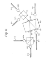
- Fig.6 shows still another embodiment of the present invention, which is the modification of the embodiment of Fig.4.
- the feature of Fig.6 is that the polarization prism blocks are separated from the interference filter blocks to allow the freedom of the design of the apparatus. Therefore, the polarization prisms 63 and 64 are separated from the interference filter block 65 as shown in the figure.
- the interference filter block 65 is provided with the interference filters 66, 67, and 68.
- the numerals 61a through 61d are optical fibers
- 61e is an optical fiber for signal light
- 61f is a transmission optical fiber
- 62a through 62f are collimating lenses.
- two linear polarization beams with the same wavelength as each other are combined (polarization multiplex) by using a polariza tion prism block. Therefore, high power pump light source is obtained even when low power semiconductor lasers are used. Furthermore, the pump light beam is directly combined with signal light to be amplified without using a lens and/or an optical fiber. Therefore, the coupling loss is small.
- the size of the apparatus may be small, and the operation of the apparatus is simple.
Applications Claiming Priority (2)
| Application Number | Priority Date | Filing Date | Title |
|---|---|---|---|
| JP260598/86 | 1986-11-04 | ||
| JP61260598A JPH0727149B2 (ja) | 1986-11-04 | 1986-11-04 | 光結合器 |
Publications (2)
| Publication Number | Publication Date |
|---|---|
| EP0268523A1 true EP0268523A1 (de) | 1988-05-25 |
| EP0268523B1 EP0268523B1 (de) | 1993-02-17 |
Family
ID=17350170
Family Applications (1)
| Application Number | Title | Priority Date | Filing Date |
|---|---|---|---|
| EP87402475A Expired - Lifetime EP0268523B1 (de) | 1986-11-04 | 1987-11-03 | Optische Einkopplungsvorrichtung für optischen Direktverstärker |
Country Status (4)
| Country | Link |
|---|---|
| US (1) | US4805977A (de) |
| EP (1) | EP0268523B1 (de) |
| JP (1) | JPH0727149B2 (de) |
| DE (1) | DE3784219T2 (de) |
Cited By (17)
| Publication number | Priority date | Publication date | Assignee | Title |
|---|---|---|---|---|
| EP0392493A1 (de) * | 1989-04-14 | 1990-10-17 | Nippon Telegraph And Telephone Corporation | Optischer Regenerator und seine Verwendung in einem optischen Netzwerk |
| EP0444694A2 (de) * | 1990-03-02 | 1991-09-04 | Fujitsu Limited | Optischer Koppler |
| EP0473071A2 (de) * | 1990-08-31 | 1992-03-04 | Sony Corporation | Vorrichtung zum Mischen von Licht aus Halbleiterlasern |
| FR2670023A1 (fr) * | 1990-12-03 | 1992-06-05 | France Etat | Dispositif pour combiner ou separer des ondes electromagnetiques de polarisations perpendiculaires entre elles, dispositif amplificateur et dispositif de detection coherente. |
| US5146516A (en) * | 1989-07-28 | 1992-09-08 | Richard Hirschmann Gmbh & Co. | Optoelectrical sending and receiving apparatus |
| EP0593205A1 (de) * | 1992-10-16 | 1994-04-20 | AT&T Corp. | Optischer Koppler |
| FR2762401A1 (fr) * | 1997-04-21 | 1998-10-23 | Nec Corp | Coupleur optique |
| EP1028333A2 (de) * | 1999-02-10 | 2000-08-16 | Fujikura Ltd. | Optische Vielfachewellenlängen-Multiplex-Vorrichtung, Vielfachewellenlängen-Lichtquelle mit einer solchen Vorrichtung und optischer Verstärker |
| EP1206018A2 (de) * | 2000-11-08 | 2002-05-15 | The Furukawa Electric Co., Ltd. | Lichtquelle mit Laserdioden-Modul |
| EP1215776A2 (de) * | 2000-11-24 | 2002-06-19 | The Furukawa Electric Co., Ltd. | Lichtquelle mit einem Halbleiterasermodul |
| WO2003005106A1 (fr) * | 2001-07-02 | 2003-01-16 | Furukawa Electric Co., Ltd | Module de laser semi-conducteur et amplificateur optique |
| WO2003012510A1 (en) * | 2001-07-27 | 2003-02-13 | Gigabit Optics Corporation | System and method for optical multiplexing and/or demultiplexing |
| EP1313182A2 (de) * | 2001-10-18 | 2003-05-21 | Tyco Telecommunications (US) Ltd. | Depolarisationsverfahren und System für optische Pumpquelle |
| DE19508100B4 (de) * | 1995-02-03 | 2004-09-02 | Storz Endoskop Gmbh | Vorrichtung zum Einkoppeln von Lichtstrahlen in eine Lichtleitfaser |
| US6872011B2 (en) | 2001-03-16 | 2005-03-29 | The Furukawa Electric Co., Ltd. | Light source having plural laser diode modules |
| EP1562311A2 (de) * | 2004-02-04 | 2005-08-10 | KT Corporation | Vorrichtung und Verfahren zur optischen Kommunikation |
| US7116479B1 (en) | 2001-07-19 | 2006-10-03 | Wavesplitter Technologies, Inc. | Array polarization beamsplitter and combiner |
Families Citing this family (70)
| Publication number | Priority date | Publication date | Assignee | Title |
|---|---|---|---|---|
| JPH0816739B2 (ja) * | 1988-12-22 | 1996-02-21 | 日本電気株式会社 | 波長分岐挿入素子 |
| JPH0327027A (ja) * | 1989-06-26 | 1991-02-05 | Oki Electric Ind Co Ltd | 光増幅器 |
| JPH0373934A (ja) * | 1989-08-15 | 1991-03-28 | Fujitsu Ltd | 光増幅器 |
| DE3929794A1 (de) * | 1989-09-07 | 1991-04-04 | Siemens Ag | Optisches sendemodul |
| US5440414A (en) * | 1990-02-02 | 1995-08-08 | The United States Of America As Represented By The Secretary Of The Navy | Adaptive polarization diversity detection scheme for coherent communications and interferometric fiber sensors |
| US5212710A (en) * | 1990-07-19 | 1993-05-18 | Sony Corporation | Laser light beam synthesizing apparatus |
| US5291571A (en) * | 1992-03-19 | 1994-03-01 | Fujitsu Limited | Duplicated light source module |
| US5309535A (en) * | 1993-04-30 | 1994-05-03 | At&T Bell Laboratories | Apparatus and method utilizing a rotating waveplate for reducing polarization dependent hole-burning in an amplified optical transmission system |
| US5309530A (en) * | 1993-04-30 | 1994-05-03 | At&T Bell Laboratories | Technique utilizing stress-induced birefringence for reducing polarization dependent hole-burning in an amplified optical transmission system |
| JPH07199236A (ja) * | 1993-12-28 | 1995-08-04 | Fujitsu Ltd | 光スイッチ及び光分配器 |
| US5471340A (en) * | 1994-01-07 | 1995-11-28 | Jds Fitel Inc. | Reflective optical non-reciprocal devices |
| US5619359A (en) * | 1994-11-16 | 1997-04-08 | Nec Research Institute, Inc. | Optoelectronic apparatus |
| DE69633476T2 (de) * | 1995-03-20 | 2005-12-01 | Fujitsu Ltd., Kawasaki | Faseroptischer Verstärker und dispersionskompensierendes Fasermodul für faseroptischen Verstärker |
| US5600467A (en) * | 1995-06-14 | 1997-02-04 | Mci Communications Corp. | Method and apparatus for reducing harmonic interference on multiplexed optical communication lines |
| US5966479A (en) * | 1996-07-09 | 1999-10-12 | Corning Incorporated | Optimized birefringent fiber switch |
| JP4063908B2 (ja) * | 1997-01-29 | 2008-03-19 | 富士通株式会社 | 光源装置、光増幅器及び光通信システム |
| JP2002501212A (ja) * | 1998-01-05 | 2002-01-15 | コーニング・インコーポレーテッド | アド/ドロップ光多重化デバイス |
| US6115174A (en) * | 1998-07-21 | 2000-09-05 | Corvis Corporation | Optical signal varying devices |
| US6344922B1 (en) * | 1998-07-21 | 2002-02-05 | Corvis Corporation | Optical signal varying devices |
| EP2306605B1 (de) * | 1998-07-23 | 2012-05-23 | The Furukawa Electric Co., Ltd. | Pumpeinheit für einen Ramanverstärker und Ramanverstärker, der dieselbe aufweist |
| US6049426A (en) * | 1998-08-17 | 2000-04-11 | New Focus, Inc. | Compact polarization insensitive circulators with simplified structure and low polarization mode dispersion |
| US6175448B1 (en) | 1998-08-17 | 2001-01-16 | New Focus, Inc. | Optical circulators using beam angle turners |
| US6212008B1 (en) | 1998-11-13 | 2001-04-03 | New Focus, Inc. | Compact polarization insensitive circulators with simplified structure and low polarization mode dispersion |
| US6147794A (en) * | 1999-02-04 | 2000-11-14 | Lucent Technologies, Inc. | Raman amplifier with pump source for improved performance |
| US6259560B1 (en) * | 1999-04-16 | 2001-07-10 | The United States Of America As Represented By The Secretary Of The Navy | Continuously variable beam combiner |
| US6587261B1 (en) * | 1999-05-24 | 2003-07-01 | Corvis Corporation | Optical transmission systems including optical amplifiers and methods of use therein |
| FR2795247B1 (fr) * | 1999-06-21 | 2001-09-14 | Cit Alcatel | Amplificateur raman a bandes multiples |
| US6611370B2 (en) * | 1999-07-23 | 2003-08-26 | The Furukawa Electric Co., Ltd. | Raman amplifier system, apparatus and method for identifying, obtaining and maintaining an arbitrary Raman amplification performance |
| US6611369B2 (en) * | 1999-09-06 | 2003-08-26 | Furukawa Electric Co., Ltd. | Optical signal amplifier |
| US6822793B2 (en) | 1999-10-29 | 2004-11-23 | Finisar Corporation | Compact polarization insensitive circulators with simplified structure and low polarization mode dispersion |
| CA2366471A1 (en) * | 2000-01-14 | 2001-07-19 | The Furukawa Electric Co., Ltd | Raman amplifier |
| US6782209B2 (en) * | 2000-03-03 | 2004-08-24 | Corvis Corporation | Optical transmission systems including optical amplifiers and methods |
| JP2003528347A (ja) * | 2000-03-17 | 2003-09-24 | コーニング インコーポレイテッド | 光導波路レンズ及び作成方法 |
| US6456425B1 (en) * | 2000-06-07 | 2002-09-24 | Tyco Telecommunications (Us) Inc. | Method and apparatus to perform lumped raman amplification |
| JP2001356377A (ja) | 2000-06-16 | 2001-12-26 | Kdd Submarine Cable Systems Inc | ポンプ光発生装置及びファイバラマン増幅器 |
| JP2002107579A (ja) | 2000-07-26 | 2002-04-10 | Furukawa Electric Co Ltd:The | 光合分波モジュール |
| US6724524B1 (en) * | 2000-08-18 | 2004-04-20 | Corning Incorporated | Gain control in Raman amplifiers |
| JP4821037B2 (ja) * | 2000-08-25 | 2011-11-24 | 富士通株式会社 | ラマン増幅を用いた光増幅器およびラマン励起光源 |
| WO2002017010A1 (fr) * | 2000-08-25 | 2002-02-28 | Fujitsu Limited | Systeme de communication optique, procede permettant de fournir de la lumiere d'excitation, et amplificateur raman distribue |
| EP1215527B1 (de) | 2000-08-30 | 2006-10-04 | Fujitsu Limited | Lichtverstärker unter verwendung der ramanverstärkung und zugehöriges steuerungsverfahren |
| JP4588282B2 (ja) * | 2000-08-31 | 2010-11-24 | 富士通株式会社 | 光通信システムの立ち上げ方法およびチャンネル増減設方法、ならびに、コンピュータ読み取り可能な記録媒体 |
| JP2002076482A (ja) | 2000-08-31 | 2002-03-15 | Fujitsu Ltd | 光増幅器,光増幅方法及び光増幅システム |
| WO2002021204A1 (en) | 2000-09-07 | 2002-03-14 | Fujitsu Limited | Optical amplifier using raman amplification |
| CN1204662C (zh) | 2000-12-15 | 2005-06-01 | 古河电气工业株式会社 | 半导体激光器模块及其制造方法和光放大器 |
| US6782028B2 (en) | 2000-12-15 | 2004-08-24 | The Furukawa Electric Co., Ltd. | Semiconductor laser device for use in a semiconductor laser module and an optical amplifier |
| JP3904835B2 (ja) * | 2001-01-29 | 2007-04-11 | 株式会社日立製作所 | 光増幅器、光ファイバラマン光増幅器、及び光システム |
| JP3768110B2 (ja) | 2001-02-22 | 2006-04-19 | 富士通株式会社 | 光増幅器 |
| JP4647807B2 (ja) | 2001-03-06 | 2011-03-09 | 富士通株式会社 | 通信システム |
| US20020167719A1 (en) * | 2001-04-20 | 2002-11-14 | Bo Pedersen | Method of pump wavelength combing for enhanced power dynamic range and redundancy broad band raman optical amplifier system |
| US6618195B2 (en) * | 2001-04-20 | 2003-09-09 | Dorsal Networks Inc. | Pump assembly employing coupled radiation sources for multiple fibers |
| JPWO2003005509A1 (ja) | 2001-07-02 | 2004-10-28 | 古河電気工業株式会社 | 半導体レーザモジュール、光増幅器及び半導体レーザモジュールの製造方法 |
| JP2004006439A (ja) | 2001-07-02 | 2004-01-08 | Furukawa Electric Co Ltd:The | 半導体レーザモジュール及びその製造方法 |
| US6704473B2 (en) | 2001-07-02 | 2004-03-09 | Chiaro Networks Ltd. | Spatial multiplexing of deflector units using polarization diversity |
| US6614586B2 (en) | 2001-07-30 | 2003-09-02 | Dorsal Networks, Inc. | Methods and systems for high performance, wide bandwidth optical communication systems using Raman amplification |
| US6571033B2 (en) * | 2001-09-28 | 2003-05-27 | Corning Incorporated | Optical signal device |
| US7196838B2 (en) * | 2001-10-03 | 2007-03-27 | Dorsal Networks, Inc. | High density optical packaging |
| US6798801B2 (en) | 2001-10-03 | 2004-09-28 | Dorsal Networks, Inc. | Pump laser current driver |
| US6671429B2 (en) | 2001-10-03 | 2003-12-30 | Dorsal Networks, Inc. | Balanced coupler for radiation sources |
| US7120362B2 (en) * | 2001-10-03 | 2006-10-10 | Bo Pedersen | High power repeaters for Raman amplified, wave division multiplexed optical communication systems |
| US6813397B2 (en) | 2001-11-21 | 2004-11-02 | Dong Lin | Micro-optic polarization beam multiplexing/de-multiplexing system |
| US6806999B2 (en) | 2001-12-06 | 2004-10-19 | Sumitomo Electric Industries, Ltd. | Raman amplification pumping module, Raman amplifier, and optical communication system |
| DE60219758T2 (de) | 2002-02-21 | 2008-01-17 | Alcatel Lucent | Faseroptisches Übertragungssystem mit Raman-Verstärkung |
| US20040208586A1 (en) * | 2002-03-27 | 2004-10-21 | Susumu Kinoshita | System and method for amplifying signals in an optical network |
| US7408867B2 (en) | 2002-04-04 | 2008-08-05 | The Furukawa Electric Co., Ltd. | Method of aligning an optical fiber, method of manufacturing a semiconductor laser module, and semiconductor laser module |
| US7006735B2 (en) * | 2002-06-04 | 2006-02-28 | Koninklijke Philips Electronics N.V. | Loss-less etendue-preserving light guides |
| US6859581B1 (en) | 2003-04-02 | 2005-02-22 | Process Instruments, Inc. | Optical fiber multiplexer for Raman spectroscopy |
| KR100701158B1 (ko) * | 2006-04-26 | 2007-03-28 | 한국전자통신연구원 | 펌프 광원이 단일 집적된 광송수신기 및 광송수신기 모듈 |
| WO2012031392A1 (zh) * | 2010-09-08 | 2012-03-15 | 青岛海信信芯科技有限公司 | 立体显示光源模块、立体显示成像装置和立体显示系统 |
| CN108227096A (zh) * | 2018-03-29 | 2018-06-29 | 四川华拓光通信股份有限公司 | 在同波长下实现收发一体的紧凑型光模块及光传输方法 |
| CN108227097A (zh) * | 2018-03-29 | 2018-06-29 | 四川华拓光通信股份有限公司 | 在同波长下实现光收发一体的光器件及光传输方法 |
Citations (2)
| Publication number | Priority date | Publication date | Assignee | Title |
|---|---|---|---|---|
| EP0146262A2 (de) * | 1983-12-16 | 1985-06-26 | Stc Plc | Optische Verstärker |
| EP0186299A2 (de) * | 1984-12-13 | 1986-07-02 | Stc Plc | Optischer Verstärker |
Family Cites Families (9)
| Publication number | Priority date | Publication date | Assignee | Title |
|---|---|---|---|---|
| JPS5650492Y2 (de) * | 1976-10-27 | 1981-11-26 | ||
| US4616898A (en) * | 1980-03-31 | 1986-10-14 | Polaroid Corporation | Optical communication systems using raman repeaters and components therefor |
| JPS56165437A (en) * | 1980-05-26 | 1981-12-19 | Kokusai Denshin Denwa Co Ltd <Kdd> | Optical repeating system for optical communication |
| FI74371C (fi) * | 1982-06-04 | 1988-01-11 | British Telecomm | Optisk oeverfoering. |
| JPS5922021A (ja) * | 1982-07-27 | 1984-02-04 | Nippon Telegr & Teleph Corp <Ntt> | 光結合器 |
| JPS59126224A (ja) * | 1983-01-07 | 1984-07-20 | Kokusai Denshin Denwa Co Ltd <Kdd> | 光フアイバの伸び分布測定法 |
| JPS60184216A (ja) * | 1984-03-02 | 1985-09-19 | Oki Electric Ind Co Ltd | 混成型光合分波器 |
| JPS6148814A (ja) * | 1984-08-16 | 1986-03-10 | Fuji Photo Film Co Ltd | レ−ザビ−ム合波装置 |
| US4566761A (en) * | 1984-09-13 | 1986-01-28 | Gte Laboratories Incorporated | Birefringent optical wavelength multiplexer/demultiplexer |
-
1986
- 1986-11-04 JP JP61260598A patent/JPH0727149B2/ja not_active Expired - Lifetime
-
1987
- 1987-11-02 US US07/115,769 patent/US4805977A/en not_active Expired - Lifetime
- 1987-11-03 DE DE8787402475T patent/DE3784219T2/de not_active Expired - Fee Related
- 1987-11-03 EP EP87402475A patent/EP0268523B1/de not_active Expired - Lifetime
Patent Citations (2)
| Publication number | Priority date | Publication date | Assignee | Title |
|---|---|---|---|---|
| EP0146262A2 (de) * | 1983-12-16 | 1985-06-26 | Stc Plc | Optische Verstärker |
| EP0186299A2 (de) * | 1984-12-13 | 1986-07-02 | Stc Plc | Optischer Verstärker |
Non-Patent Citations (3)
| Title |
|---|
| PATENT ABSTRACTS OF JAPAN, vol. 6, no. 13 (P.99)[891]. 26th January 1982; & JP - A - 56 137 303 (MITSUBISHI DENKI K.K.) 27-10-1981 * |
| PATENT ABSTRACTS OF JAPAN, vol. 7, no. 182 (E-192)[1327], 11th August 1983; & JP - A - 58 85588 (NIPPON DENKI K.K.) 21-05-1983 * |
| PATENT ABSTRACTS OF JAPAN, vol. 8, no. 125 (P-279)[1562], 12th June 1984; & JP - A - 59 29219 (NIPPON DENSHIN DENWA KOSHA) 16-02-1984 * |
Cited By (39)
| Publication number | Priority date | Publication date | Assignee | Title |
|---|---|---|---|---|
| EP0392493A1 (de) * | 1989-04-14 | 1990-10-17 | Nippon Telegraph And Telephone Corporation | Optischer Regenerator und seine Verwendung in einem optischen Netzwerk |
| US5083874A (en) * | 1989-04-14 | 1992-01-28 | Nippon Telegraph And Telephone Corporation | Optical repeater and optical network using the same |
| US5146516A (en) * | 1989-07-28 | 1992-09-08 | Richard Hirschmann Gmbh & Co. | Optoelectrical sending and receiving apparatus |
| EP0444694A3 (en) * | 1990-03-02 | 1992-09-02 | Fujitsu Limited | Optical coupler |
| EP0444694A2 (de) * | 1990-03-02 | 1991-09-04 | Fujitsu Limited | Optischer Koppler |
| EP0473071A3 (en) * | 1990-08-31 | 1992-04-29 | Sony Corporation | Wave combining apparatus for semiconductor laser |
| EP0473071A2 (de) * | 1990-08-31 | 1992-03-04 | Sony Corporation | Vorrichtung zum Mischen von Licht aus Halbleiterlasern |
| US5210643A (en) * | 1990-08-31 | 1993-05-11 | Sony Corporation | Wave combining apparatus for semiconductor lasers |
| FR2670023A1 (fr) * | 1990-12-03 | 1992-06-05 | France Etat | Dispositif pour combiner ou separer des ondes electromagnetiques de polarisations perpendiculaires entre elles, dispositif amplificateur et dispositif de detection coherente. |
| EP0593205A1 (de) * | 1992-10-16 | 1994-04-20 | AT&T Corp. | Optischer Koppler |
| DE19508100B4 (de) * | 1995-02-03 | 2004-09-02 | Storz Endoskop Gmbh | Vorrichtung zum Einkoppeln von Lichtstrahlen in eine Lichtleitfaser |
| FR2762401A1 (fr) * | 1997-04-21 | 1998-10-23 | Nec Corp | Coupleur optique |
| EP1028333A3 (de) * | 1999-02-10 | 2002-07-31 | Fujikura Ltd. | Optische Vielfachewellenlängen-Multiplex-Vorrichtung, Vielfachewellenlängen-Lichtquelle mit einer solchen Vorrichtung und optischer Verstärker |
| US6459829B1 (en) | 1999-02-10 | 2002-10-01 | Ryozo Yamauchi | Multiple wavelength excitation optical multiplexing device, multiple wavelength excitation light source incorporating aforementioned device, and optical amplifier |
| EP1028333A2 (de) * | 1999-02-10 | 2000-08-16 | Fujikura Ltd. | Optische Vielfachewellenlängen-Multiplex-Vorrichtung, Vielfachewellenlängen-Lichtquelle mit einer solchen Vorrichtung und optischer Verstärker |
| EP1206018A2 (de) * | 2000-11-08 | 2002-05-15 | The Furukawa Electric Co., Ltd. | Lichtquelle mit Laserdioden-Modul |
| EP1206018A3 (de) * | 2000-11-08 | 2002-11-06 | The Furukawa Electric Co., Ltd. | Lichtquelle mit Laserdioden-Modul |
| US6839367B2 (en) | 2000-11-08 | 2005-01-04 | The Furukawa Electric Co., Ltd. | Light source comprising laser diode module |
| US6876681B2 (en) | 2000-11-24 | 2005-04-05 | The Furukawa Electric Co., Ltd. | Light source comprising laser diode module |
| EP1215776A2 (de) * | 2000-11-24 | 2002-06-19 | The Furukawa Electric Co., Ltd. | Lichtquelle mit einem Halbleiterasermodul |
| EP1215776A3 (de) * | 2000-11-24 | 2004-03-24 | The Furukawa Electric Co., Ltd. | Lichtquelle mit einem Halbleiterasermodul |
| US6872011B2 (en) | 2001-03-16 | 2005-03-29 | The Furukawa Electric Co., Ltd. | Light source having plural laser diode modules |
| CN1306318C (zh) * | 2001-07-02 | 2007-03-21 | 古河电气工业株式会社 | 半导体激光组件与光放大器 |
| US7085440B2 (en) | 2001-07-02 | 2006-08-01 | The Furukawa Electric Co., Ltd | Semiconductor laser module and optical amplifier |
| WO2003005106A1 (fr) * | 2001-07-02 | 2003-01-16 | Furukawa Electric Co., Ltd | Module de laser semi-conducteur et amplificateur optique |
| US7116479B1 (en) | 2001-07-19 | 2006-10-03 | Wavesplitter Technologies, Inc. | Array polarization beamsplitter and combiner |
| WO2003012510A1 (en) * | 2001-07-27 | 2003-02-13 | Gigabit Optics Corporation | System and method for optical multiplexing and/or demultiplexing |
| US6847450B2 (en) | 2001-07-27 | 2005-01-25 | Oplink Communications, Inc. | System and method for optical multiplexing and/or demultiplexing |
| US6856435B2 (en) | 2001-07-27 | 2005-02-15 | Gigabit Optics Corporation | System and method for optical multiplexing and/or demultiplexing |
| US6844932B2 (en) | 2001-07-27 | 2005-01-18 | Oplink Communications, Inc. | System and method for optical multiplexing and/or demultiplexing |
| US6781693B2 (en) | 2001-07-27 | 2004-08-24 | Gigabit Optics Corporation | System and method for optical multiplexing and/or demultiplexing |
| US6914676B2 (en) | 2001-07-27 | 2005-07-05 | Oplink Communications, Inc. | System and method for optical multiplexing and/or demultiplexing |
| US6750969B2 (en) | 2001-07-27 | 2004-06-15 | Gigabit Optics Corporation | System and method for optical multiplexing and/or demultiplexing |
| EP1313182A3 (de) * | 2001-10-18 | 2003-08-27 | Tyco Telecommunications (US) Ltd. | Depolarisationsverfahren und System für optische Pumpquelle |
| EP1313182A2 (de) * | 2001-10-18 | 2003-05-21 | Tyco Telecommunications (US) Ltd. | Depolarisationsverfahren und System für optische Pumpquelle |
| EP1562311A2 (de) * | 2004-02-04 | 2005-08-10 | KT Corporation | Vorrichtung und Verfahren zur optischen Kommunikation |
| EP1562311A3 (de) * | 2004-02-04 | 2006-05-24 | KT Corporation | Vorrichtung und Verfahren zur optischen Kommunikation |
| US7197206B2 (en) | 2004-02-04 | 2007-03-27 | Kt Corporation | Optical communication system and method thereof |
| KR100945137B1 (ko) * | 2004-02-04 | 2010-03-02 | 주식회사 케이티 | 광통신 시스템 및 그 방법 |
Also Published As
| Publication number | Publication date |
|---|---|
| JPH0727149B2 (ja) | 1995-03-29 |
| EP0268523B1 (de) | 1993-02-17 |
| US4805977A (en) | 1989-02-21 |
| DE3784219T2 (de) | 1993-06-09 |
| JPS63115145A (ja) | 1988-05-19 |
| DE3784219D1 (de) | 1993-03-25 |
Similar Documents
| Publication | Publication Date | Title |
|---|---|---|
| EP0268523A1 (de) | Optische Einkopplungsvorrichtung für optischen Direktverstärker | |
| US5231529A (en) | Light amplifier for multi-wavelength signals | |
| US5125053A (en) | Optical coupler ultizing prisms | |
| US6760160B2 (en) | Fiber optic isolator for use with multiple-wavelength optical signals | |
| US5657155A (en) | Optical tap coupler device | |
| JP3778641B2 (ja) | 光増幅器 | |
| JP2991131B2 (ja) | 信号光チャネル数計数器とこれを用いた光増幅装置 | |
| US5974212A (en) | Optical line monitor and optical amplification apparatus using same | |
| JP3754728B2 (ja) | 光デバイス | |
| US6839485B2 (en) | Optical device for compensation of multiple wavelengths and working distances in dual-fiber collimators | |
| JPH09326520A (ja) | 光フィルタモジュールおよびそれを用いた光増幅装置 | |
| US6144785A (en) | Light source with WDM function, and optical amplifier and two-way optical transmission apparatus applied therewith | |
| US6389192B1 (en) | Light source with WDM function, and optical amplifier and two-way optical transmission apparatus applied therewith | |
| US6236497B1 (en) | Direct free space pump signal mixing for EDFA | |
| JPS58115948A (ja) | 双方向光増幅器 | |
| JP3000900B2 (ja) | 光カプラ | |
| JP2576408B2 (ja) | 光分波器 | |
| JPS5815926Y2 (ja) | 複合型光波長分波回路 | |
| EP0939465A2 (de) | Lichtquelle mit WDM-Funktion, optischer Verstärker und bidirektionales Ubertragungssystem unter Verwndung derselben | |
| JPH0311322A (ja) | 双方向光増幅伝送回路 | |
| US7139447B1 (en) | Angular dispersion amplification method and apparatus for optical demultiplexing | |
| JPS62170932A (ja) | 波長多重伝送方式 | |
| JP2905767B1 (ja) | 光部品 | |
| JPH04369627A (ja) | 光ファイバ増幅用合波モジュールおよびそれを用いた光 ファイバ増幅器 | |
| JPH0355508A (ja) | レーザダイオードモジュール |
Legal Events
| Date | Code | Title | Description |
|---|---|---|---|
| PUAI | Public reference made under article 153(3) epc to a published international application that has entered the european phase |
Free format text: ORIGINAL CODE: 0009012 |
|
| AK | Designated contracting states |
Kind code of ref document: A1 Designated state(s): DE FR GB IT |
|
| 17P | Request for examination filed |
Effective date: 19881118 |
|
| 17Q | First examination report despatched |
Effective date: 19910225 |
|
| RTI1 | Title (correction) | ||
| GRAA | (expected) grant |
Free format text: ORIGINAL CODE: 0009210 |
|
| AK | Designated contracting states |
Kind code of ref document: B1 Designated state(s): DE FR GB IT |
|
| REF | Corresponds to: |
Ref document number: 3784219 Country of ref document: DE Date of ref document: 19930325 |
|
| ITF | It: translation for a ep patent filed |
Owner name: JACOBACCI CASETTA & PERANI S.P.A. |
|
| ET | Fr: translation filed | ||
| PLBE | No opposition filed within time limit |
Free format text: ORIGINAL CODE: 0009261 |
|
| STAA | Information on the status of an ep patent application or granted ep patent |
Free format text: STATUS: NO OPPOSITION FILED WITHIN TIME LIMIT |
|
| 26N | No opposition filed | ||
| PGFP | Annual fee paid to national office [announced via postgrant information from national office to epo] |
Ref country code: GB Payment date: 19981106 Year of fee payment: 12 Ref country code: DE Payment date: 19981106 Year of fee payment: 12 |
|
| PGFP | Annual fee paid to national office [announced via postgrant information from national office to epo] |
Ref country code: FR Payment date: 19981110 Year of fee payment: 12 |
|
| PG25 | Lapsed in a contracting state [announced via postgrant information from national office to epo] |
Ref country code: GB Free format text: LAPSE BECAUSE OF NON-PAYMENT OF DUE FEES Effective date: 19991103 |
|
| GBPC | Gb: european patent ceased through non-payment of renewal fee |
Effective date: 19991103 |
|
| PG25 | Lapsed in a contracting state [announced via postgrant information from national office to epo] |
Ref country code: FR Free format text: LAPSE BECAUSE OF NON-PAYMENT OF DUE FEES Effective date: 20000731 |
|
| PG25 | Lapsed in a contracting state [announced via postgrant information from national office to epo] |
Ref country code: DE Free format text: LAPSE BECAUSE OF NON-PAYMENT OF DUE FEES Effective date: 20000901 |
|
| REG | Reference to a national code |
Ref country code: FR Ref legal event code: ST |
|
| PG25 | Lapsed in a contracting state [announced via postgrant information from national office to epo] |
Ref country code: IT Free format text: LAPSE BECAUSE OF NON-PAYMENT OF DUE FEES;WARNING: LAPSES OF ITALIAN PATENTS WITH EFFECTIVE DATE BEFORE 2007 MAY HAVE OCCURRED AT ANY TIME BEFORE 2007. THE CORRECT EFFECTIVE DATE MAY BE DIFFERENT FROM THE ONE RECORDED. Effective date: 20051103 |