EP0267017B1 - Circuit de tampon d'entrée compatible TTL/CMOS - Google Patents
Circuit de tampon d'entrée compatible TTL/CMOS Download PDFInfo
- Publication number
- EP0267017B1 EP0267017B1 EP87309753A EP87309753A EP0267017B1 EP 0267017 B1 EP0267017 B1 EP 0267017B1 EP 87309753 A EP87309753 A EP 87309753A EP 87309753 A EP87309753 A EP 87309753A EP 0267017 B1 EP0267017 B1 EP 0267017B1
- Authority
- EP
- European Patent Office
- Prior art keywords
- voltage
- channel transistor
- input
- ttl
- schmitt trigger
- Prior art date
- Legal status (The legal status is an assumption and is not a legal conclusion. Google has not performed a legal analysis and makes no representation as to the accuracy of the status listed.)
- Expired - Lifetime
Links
Images

Classifications
-
- H—ELECTRICITY
- H03—ELECTRONIC CIRCUITRY
- H03K—PULSE TECHNIQUE
- H03K3/00—Circuits for generating electric pulses; Monostable, bistable or multistable circuits
- H03K3/02—Generators characterised by the type of circuit or by the means used for producing pulses
- H03K3/353—Generators characterised by the type of circuit or by the means used for producing pulses by the use, as active elements, of field-effect transistors with internal or external positive feedback
- H03K3/356—Bistable circuits
- H03K3/3565—Bistables with hysteresis, e.g. Schmitt trigger
-
- H—ELECTRICITY
- H03—ELECTRONIC CIRCUITRY
- H03K—PULSE TECHNIQUE
- H03K19/00—Logic circuits, i.e. having at least two inputs acting on one output; Inverting circuits
- H03K19/003—Modifications for increasing the reliability for protection
- H03K19/00346—Modifications for eliminating interference or parasitic voltages or currents
- H03K19/00361—Modifications for eliminating interference or parasitic voltages or currents in field effect transistor circuits
-
- H—ELECTRICITY
- H03—ELECTRONIC CIRCUITRY
- H03K—PULSE TECHNIQUE
- H03K19/00—Logic circuits, i.e. having at least two inputs acting on one output; Inverting circuits
- H03K19/0175—Coupling arrangements; Interface arrangements
- H03K19/0185—Coupling arrangements; Interface arrangements using field effect transistors only
- H03K19/018507—Interface arrangements
- H03K19/018521—Interface arrangements of complementary type, e.g. CMOS
Definitions
- This invention relates to a TTL/CMOS compatible input buffer.
- U.S. Patent Application 778,344 filed September 19, 1985 on which Patent US-A-4 820 937 issued on 11 April 1989 discloses a transistor-transistor logic/complementary-metal-oxide semiconductor (TTL/CMOS) input buffer.
- TTL/CMOS transistor-transistor logic/complementary-metal-oxide semiconductor
- the input buffer has high speed, low or no DC power dissipation at TTL input levels, and no DC power dissipation at CMOS input levels.
- CMOS inverter In order to distinguish between a logical 0 and a logical 1 a CMOS inverter must be capable of switching somewhere between 0.8 and 2.0 volts and preferably at approximately 1.4 volts in order to provide the widest possible noise margin.
- a CMOS inverter generally operates at voltages of 4.5 to 15 volts with 5 volts being typical.
- the P-channel transistor in the CMOS inverter will draw a steady state current when a TTL logical "1" as low as 2.0 volts is applied to its gate.
- U.S. Patent US-A-4 471 242 describes a TTL/CMOS input buffer that accomplishes buffering a TTL signal to a CMOS signal with low current flow through a CMOS input inverter in a static (nonswitching) condition. This is achieved by providing a selected reference voltage to the source of the P-channel transistor in the CMOS input inverter. The reference voltage is selected to be less than the lowest voltage level of the TTL logical "1" (2.0 volts) minus the threshold voltage of the P-channel transistor.
- US-A-4 475 050 describes prevention of current flow through the CMOS inverter of the TTL to CMOS input buffer by providing a reference voltage to the source of the P-channel transistor in the input inverter which is responsive to the voltage level of the TTL input signal.
- US-A-4 469 959 describes a bypass means that compensates for the body effect of the load transistor to maintain the switch point of the input inverter stage at a relatively constant value.
- US-A-4 563 595 describes a TTL/CMOS compatible input buffer network comprising a Schmitt trigger circuit having a higher trigger point to rising input signals and a lower trigger point to falling input signals, the Schmitt trigger circuit having an input line for receiving an input signal, an output line for providing an output signal, a first supply terminal for connection to a first supply voltage, and a second supply terminal for receiving a reference voltage (V REF ).
- the present invention provides a TTL/CMOS compatible input buffer network of the kind described in US-A-4 563 595 characterised by a reference stage reflecting the Schmitt trigger circuit (10) and having trigger points matching those of the Schmitt trigger circuit, the reference stage having supply terminals for receiving said first supply voltage and said reference voltage, input and output lines (T2A) matching those of the Schmitt trigger circuit but connected so that the input and output lines (T2A) of the reference stage provide a feedback voltage which is between the trigger points of the Schmitt trigger circuit; and a voltage control circuit (P3) which receives a second supply voltage (Vcc), a selected voltage and the feedback voltage, and which generates the reference voltage (V REF ) so that the feedback voltage is equal to the selected voltage.
- Vcc second supply voltage
- V REF reference voltage
- a TTL/CMOS compatible input buffer comprises a Schmitt trigger 10 and a reference voltage generator 20.
- the reference voltage generator 20 provides a reference voltage to establish the trigger point of the Schmitt trigger to be at the desired level of approximately 1.4 volts.
- the Schmitt trigger 10 has a hysteresis characteristic that effectively enhances noise immunity, and is used in the input buffer circuit of this invention to replace the inverter circuit incorporated in the input buffer disclosed in the aforementioned copending patent application.
- the Schmitt trigger includes a P-channel enhancement transistor M1 and N-channel enhancement transistors M2, M3 and M4.
- the gate electrodes of transistors M1, M2 and M3 are connected to receive an input signal V IN through lead 13, and the drains of transistors M1 and M2 are connected to the gate of transistor M4 to couple to an output terminal V OUT through lead 16.
- the source of transistors M1 is connected to the drain of transistor M4 to couple to the reference voltage generator 20 through lead 21.
- the drain of transistor M3 is connected to the source of transistors M2 and M4.
- the source of transistor M3 is connected to a reference potential or ground.
- the input buffer When the input buffer operates in the TTL mode, i.e. when the signals on input lead V IN of the input buffer are at TTL levels switching between 0.8 volts and 2.0 volts, one desirable voltage level of reference voltage V REF on output lead 21 is approximately 3.5 volts.
- V REF reference voltage
- the DC power loss is the power loss resulting from the steady state current that flows from the reference generator 20 through transistors M1, M2 and M3 to ground.
- the trigger or trip point which is a function of V REF
- the trigger or trip point should be at or near the midpoint of the TTL voltage levels, which is approximately 1.4 volts.
- the Schmitt trigger operates at two trigger voltage levels, one trigger occurring at the rising edge of the input signal and the second trigger occurring at the falling edge of the input signal.
- a larger noise margin is obtained by virtue of the two distinct trigger voltages which are centered about the desired 1.4 volt level.
- both voltages at node T2 and node T3 are 0 volts and transistor M4 is nonconducting or off.
- the voltage at node T2 and at node T3 both rise.
- the voltage difference between the input V IN and that at terminal T3 is less than the voltage V t (M2)
- transistor M2 cuts off and the voltage at terminal T2 rises rapidly to the reference voltage V REF and transistor M4 is turned on.
- the DC characteristic of the Schmitt trigger is then determined by transistors M3 and M4 that provide a higher trigger point than the inverter comprising transistors M1, M2 and M3.
- a power down (PD) control signal is applied to transistor P4 of the reference voltage generator 20.
- P4 is coupled to a voltage supply V cc and to ground potential through series resistors R1 and R2.
- Resistor R1 has a resistance value greater than that of R2, in this implementation, being in the ratio of 5R:2R, by way of example.
- the resistance values are selected so that the reference voltage at node T1A is at the midpoint of the range of TTL values, that is at 1.4 Volts approximately.
- the reference voltage on node T1A is substantially equal to the desired trigger point of the Schmitt trigger 10, which is the selected value between the low level TTL signal (0.8 Volts) and the high level TTL signal (2.0 Volts).
- the voltage at node T1A is applied to the inverting input lead 26 of operational amplifier 25.
- Capacitor C1 which is connected between T1A and ground smooths any glitches that may be caused by power supply perturbations.
- the noninverting input lead 27 of the op amp 25 is connected to the output node T2A of the reference input buffer stage 11A of the reference voltage generator.
- the reference input buffer stage 11A comprises a P-channel transistor P2, an N-channel transistor N2, an N-channel transistor N3, and an N-channel transistor N4.
- the configuration of the reference input buffer stage 11A is substantially equivalent to that of the Schmitt trigger 10, except that the node T2A is shorted to the gates of P2, N2 and N3.
- the ratios of the sizes of the transistors P2, N2, N3 and N4 are substantially the same as the ratios of sizes of transistors M1, M2, M3 and M4, respectively.
- the output signal of the operational amplifier 25 controls the gate of a P-channel transistor P3, which is a relatively large transistor.
- the transistor P3 acts as a true voltage source and limits excursions of the voltage at node T3A.
- P3 supplies transient current for all input buffers in the system, which are similar to the Schmitt trigger input buffer 29 and connected to the output lead 21 of the reference voltage generator 20.
- a capacitor C2 which is a large capacitor having a capacitance value of 50 picoFarads, by way of example, is connected to output lead 21 of the reference voltage generator 20 and serves to stabilize the reference voltage.
- the Schmitt trigger input buffer 29 includes an output stage comprising an inverter formed with a P-channel transistor M5 and N-channel transistor M6.
- the transistor M5 is a native P-channel transistor having a threshold voltage of about -1.6 Volts ⁇ 0.2 Volts, so that the inverter formed by the M5 and M6 transistors does not consume DC power when V REF has a value greater than or equal to 3.5 Volts approximately.
- the trigger point of the reference input buffer is in effect the voltage at node T2A, which is connected to the noninverting lead 27 at the input of op amp 25.
- the output signal from the op amp 25 is fed to the gate of P3 to establish a reference voltage at node T3A so that the voltage at the node T2A approaches the desired level of about 1.4 volts.
- the trigger point of the Schmitt trigger is the same as the trigger point of the reference input buffer, which is at the desired approximate 1.4 volt level.
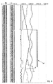
- Fig. 2 illustrates two waveforms, representing the reference voltage V REF , and the trigger voltage V TRIG with slow input transitions and a noisy reference voltage that produces an indeterminate output signal.
- a feature of the invention is that the Schmitt trigger input buffer with its hysteresis characteristic overcomes the effect of the slow input transitions.
- the hysteresis of the Schmitt trigger which is controlled by the transistor sizes, causes a change in the threshold level of the trigger.
- the Schmitt trigger is characterized by two trigger points which are higher and lower than the desired 1.4 volt trigger level respectively. The trigger points are switched in response to the rising and falling edges of the input signal V IN .
- Figs. 3a and 3b show the transfer curves for a normal inverter and a Schmitt trigger respectively, illustrating the hysteresis characteristic of the Schmitt trigger.
- Figure 4 represents a computer simulation obtained by simulating the operation of the Schmitt trigger input buffer in a noisy reference voltage environment.
- the input buffer of this invention affords better noise immunity and improves the tolerance to the noise level of the reference voltage, thereby increasing the reliability of the input buffer even when the input signal has a very slow transition time.
Landscapes
- Engineering & Computer Science (AREA)
- Computer Hardware Design (AREA)
- Physics & Mathematics (AREA)
- Computing Systems (AREA)
- General Engineering & Computer Science (AREA)
- Mathematical Physics (AREA)
- Logic Circuits (AREA)
Claims (7)
- Réseau d'entrée intermédiaire compatible avec TTL/CMOS comprenant
un circuit de déclenchement Schmitt (10) présentant un point de déclenchement haut pour les signaux d'entrée en augmentation et un point de déclenchement bas pour les signaux d'entrée en diminution, le circuit de déclenchement Schmitt ayant une ligne d'entrée (13) devant recevoir un signal d'entrée (VIN), une ligne de sortie (T2) devant fournir un signal de sortie, une première borne d'alimentation pour une connexion à une première tension d'alimentation et une seconde borne d'alimentation (21) devant recevoir une tension de référence (VREF), caractérisé par
un étage de référence (11A) réfléchissant le circuit de déclenchement Schmitt (10) et présentant des points de déclenchement correspondant à ceux du circuit de déclenchement Schmitt (10), l'étage de référence ayant des bornes d'alimentation devant recevoir ladite première tension d'alimentation et ladite tension de référence (VREF), des lignes d'entrée et de sortie (T2A) correspondant à celles du circuit de déclenchement Schmitt mais connectées de telle sorte que les lignes d'entrée et de sortie (T2A) de l'étage de référence fournissent une tension à réaction située entre les points de déclenchement du circuit de déclenchement Schmitt; et
un circuit de commande de tension (25, P3) qui reçoit une seconde tension d'alimentation (Vcc), une tension sélectionnée et la tension à réaction, et qui génère la tension de référence (VREF) de telle sorte que la tension à réaction soit égale à la tension sélectionnée. - Réseau d'entrée intermédiaire compatible avec TTL/CMOS selon la revendication 1 où le circuit de déclenchement Schmitt (10) comporte un transistor à canal P (M1), un premier transistor à canal N (M2), un second transistor à canal N (M3) et un troisième transistor à canal N (M4), les électrodes de porte du transistor à canal P, du premier transistor à canal N et du second transistor à canal N étant connectées à la ligne d'entrée, les électrodes de drain du transistor à canal P et du premier transistor à canal N étant connectées à la ligne de sortie, le drain du second transistor à canal N et la source du premier transistor à canal N étant connectés à un branchement (T3), la source du second transistor à canal N étant connectée à la premier tension d'alimentation, la porte du troisième transistor à canal N étant connectée à la ligne de sortie, le drain du troisième transistor à canal N étant connecté à la source du transistor à canal P et à la second borne d'alimentation, et la source du troisième transistor à canal N étant connectée au branchement (T3).
- Réseau d'entrée intermédiaire compatible avec TTL/CMOS selon la revendication 1 ou 2 comportant un étage de sortie d'onduleur (M5, M6) accouplé à la ligne de sortie du circuit de déclenchement Schmitt (10) afin de fournir pour exploitation un signal de sortie de tension prédéterminée.
- Réseau d'entrée intermédiaire compatible avec TTL/CMOS selon la revendication 1, 2 ou 3 comportant un branchement de générateur de tension (T1A) situé entre deux résistances (R1, R2) connectées en série, une résistance étant accouplée à la première tension d'alimentation et l'autre résistance étant accouplée à la seconde tension d'alimentation, le branchement du générateur de tension fournissant la tension sélectionnée (T1A).
- Réseau d'entrée intermédiaire compatible avec TTL/CMOS selon la revendication 4 où l'autre résistance est accouplée à la seconde tension d'alimentation par l'intermédiaire d'un transistor (P4).
- Réseau d'entrée intermédiaire compatible avec TTL/CMOS selon toute revendication précédente comportant un grand condensateur (C2) lié à un second branchement (T3A) afin de fournir la tension de référence (VREF) pour amortir le bruit.
- Réseau d'entrée intermédiaire compatible avec TTL/CMOS selon toute revendication précédente où le circuit de commande de tension comporte:
un grand transistor (P3) offrant une borne porteuse de courant connectée à une seconde tension d'alimentation (Vcc) et une seconde borne porteuse de courant destinée à fournir la tension de référence (VREF); et
un amplificateur opérationnel (25) qui reçoit la tension sélectionnée sur une borne d'entrée, la tension à réaction sur l'autre borne d'entrée et qui fournit sur sa borne de sortie un signal de commande destiné à contrôler le grand transistor (P3).
Applications Claiming Priority (2)
| Application Number | Priority Date | Filing Date | Title |
|---|---|---|---|
| US06/927,289 US4783607A (en) | 1986-11-05 | 1986-11-05 | TTL/CMOS compatible input buffer with Schmitt trigger |
| US927289 | 1986-11-05 |
Publications (2)
| Publication Number | Publication Date |
|---|---|
| EP0267017A1 EP0267017A1 (fr) | 1988-05-11 |
| EP0267017B1 true EP0267017B1 (fr) | 1994-03-02 |
Family
ID=25454525
Family Applications (1)
| Application Number | Title | Priority Date | Filing Date |
|---|---|---|---|
| EP87309753A Expired - Lifetime EP0267017B1 (fr) | 1986-11-05 | 1987-11-04 | Circuit de tampon d'entrée compatible TTL/CMOS |
Country Status (4)
| Country | Link |
|---|---|
| US (2) | US4783607A (fr) |
| EP (1) | EP0267017B1 (fr) |
| JP (1) | JP2555379B2 (fr) |
| DE (1) | DE3789199T2 (fr) |
Families Citing this family (43)
| Publication number | Priority date | Publication date | Assignee | Title |
|---|---|---|---|---|
| US4841175A (en) * | 1987-01-23 | 1989-06-20 | Siemens Aktiengesellschaft | ECL-compatible input/output circuits in CMOS technology |
| US4763021A (en) * | 1987-07-06 | 1988-08-09 | Unisys Corporation | CMOS input buffer receiver circuit with ultra stable switchpoint |
| KR900001817B1 (ko) * | 1987-08-01 | 1990-03-24 | 삼성전자 주식회사 | 저항 수단을 이용한 씨 모스 티티엘 인푸트 버퍼 |
| US5280200A (en) * | 1989-04-10 | 1994-01-18 | Tarng Min M | Pipelined buffer for analog signal and power supply |
| US4999529A (en) * | 1989-06-30 | 1991-03-12 | At&T Bell Laboratories | Programmable logic level input buffer |
| US5008570A (en) * | 1990-03-30 | 1991-04-16 | The United States Of America As Represented By The Secretary Of The Air Force | Schmitt-triggered TTL to CML input buffer apparatus |
| US5322812A (en) * | 1991-03-20 | 1994-06-21 | Crosspoint Solutions, Inc. | Improved method of fabricating antifuses in an integrated circuit device and resulting structure |
| US5444405A (en) | 1992-03-02 | 1995-08-22 | Seiko Epson Corporation | Clock generator with programmable non-overlapping clock edge capability |
| US5410189A (en) * | 1993-09-27 | 1995-04-25 | Xilinx, Inc. | Input buffer having an accelerated signal transition |
| KR0126254B1 (ko) * | 1993-10-06 | 1998-04-10 | 김광호 | 반도체 메모리 장치의 데이터 입력 버퍼 |
| US5436588A (en) * | 1993-12-17 | 1995-07-25 | National Semiconductor Corp. | Click/pop free bias circuit |
| US5469111A (en) * | 1994-08-24 | 1995-11-21 | National Semiconductor Corporation | Circuit for generating a process variation insensitive reference bias current |
| US5510729A (en) * | 1995-03-27 | 1996-04-23 | General Datacomm, Inc. | Output characteristics stabilization of CMOS devices |
| US5970255A (en) | 1995-10-16 | 1999-10-19 | Altera Corporation | System for coupling programmable logic device to external circuitry which selects a logic standard and uses buffers to modify output and input signals accordingly |
| JP3612634B2 (ja) * | 1996-07-09 | 2005-01-19 | 富士通株式会社 | 高速クロック信号に対応した入力バッファ回路、集積回路装置、半導体記憶装置、及び集積回路システム |
| US5877632A (en) | 1997-04-11 | 1999-03-02 | Xilinx, Inc. | FPGA with a plurality of I/O voltage levels |
| KR100263667B1 (ko) * | 1997-12-30 | 2000-08-01 | 김영환 | 슈미트 트리거 회로 |
| US6433579B1 (en) | 1998-07-02 | 2002-08-13 | Altera Corporation | Programmable logic integrated circuit devices with differential signaling capabilities |
| US6346827B1 (en) | 1998-09-09 | 2002-02-12 | Altera Corporation | Programmable logic device input/output circuit configurable as reference voltage input circuit |
| US6133772A (en) | 1998-12-14 | 2000-10-17 | Ati International Srl | Differential input receiver and method for reducing noise |
| US6472903B1 (en) | 1999-01-08 | 2002-10-29 | Altera Corporation | Programmable logic device input/output architecture with power bus segmentation for multiple I/O standards |
| US6271679B1 (en) | 1999-03-24 | 2001-08-07 | Altera Corporation | I/O cell configuration for multiple I/O standards |
| US6836151B1 (en) | 1999-03-24 | 2004-12-28 | Altera Corporation | I/O cell configuration for multiple I/O standards |
| US6246258B1 (en) | 1999-06-21 | 2001-06-12 | Xilinx, Inc. | Realizing analog-to-digital converter on a digital programmable integrated circuit |
| US6476638B1 (en) * | 2001-06-07 | 2002-11-05 | Xilinx, Inc. | Input driver circuit with adjustable trip point for multiple input voltage standards |
| JP3680122B2 (ja) * | 2001-08-10 | 2005-08-10 | シャープ株式会社 | 基準電圧発生回路 |
| US6911860B1 (en) | 2001-11-09 | 2005-06-28 | Altera Corporation | On/off reference voltage switch for multiple I/O standards |
| US7307446B1 (en) | 2003-01-07 | 2007-12-11 | Altera Corporation | Integrated circuit output driver circuitry with programmable preemphasis |
| US6831480B1 (en) | 2003-01-07 | 2004-12-14 | Altera Corporation | Programmable logic device multispeed I/O circuitry |
| US6940302B1 (en) * | 2003-01-07 | 2005-09-06 | Altera Corporation | Integrated circuit output driver circuitry with programmable preemphasis |
| US7023238B1 (en) | 2004-01-07 | 2006-04-04 | Altera Corporation | Input buffer with selectable threshold and hysteresis option |
| US6958679B1 (en) | 2004-02-05 | 2005-10-25 | Xilinx, Inc. | Binary hysteresis equal comparator circuits and methods |
| US7053687B1 (en) | 2004-02-05 | 2006-05-30 | Xilinx, Inc. | Binary hysteresis comparator circuits and methods |
| US6965251B1 (en) | 2004-02-18 | 2005-11-15 | Altera Corporation | Input buffer with hysteresis option |
| US7598779B1 (en) | 2004-10-08 | 2009-10-06 | Altera Corporation | Dual-mode LVDS/CML transmitter methods and apparatus |
| US7365570B2 (en) * | 2005-05-25 | 2008-04-29 | Micron Technology, Inc. | Pseudo-differential output driver with high immunity to noise and jitter |
| US7265587B1 (en) | 2005-07-26 | 2007-09-04 | Altera Corporation | LVDS output buffer pre-emphasis methods and apparatus |
| US20070103210A1 (en) * | 2005-11-07 | 2007-05-10 | Taiwan Semiconductor Manufacturing Company, Ltd. | Power-on reset circuit for an integrated circuit |
| US7953162B2 (en) * | 2006-11-17 | 2011-05-31 | Intersil Americas Inc. | Use of differential pair as single-ended data paths to transport low speed data |
| US7868658B1 (en) | 2008-01-11 | 2011-01-11 | Marvell International Ltd. | Level shifter circuits and methods for maintaining duty cycle |
| US7733118B2 (en) * | 2008-03-06 | 2010-06-08 | Micron Technology, Inc. | Devices and methods for driving a signal off an integrated circuit |
| CN104393868A (zh) * | 2014-12-22 | 2015-03-04 | 厦门福齐电子科技有限公司 | 一种输入接口集成电路及其输入接口电路 |
| TWI767773B (zh) * | 2021-06-30 | 2022-06-11 | 緯穎科技服務股份有限公司 | 入侵偵測裝置及其方法 |
Family Cites Families (19)
| Publication number | Priority date | Publication date | Assignee | Title |
|---|---|---|---|---|
| US4032795A (en) * | 1976-04-14 | 1977-06-28 | Solitron Devices, Inc. | Input buffer |
| DE2708021C3 (de) * | 1977-02-24 | 1984-04-19 | Eurosil GmbH, 8000 München | Schaltungsanordnung in integrierter CMOS-Technik zur Regelung der Speisespannung für eine Last |
| US4258272A (en) * | 1979-03-19 | 1981-03-24 | National Semiconductor Corporation | TTL to CMOS input buffer circuit |
| US4438352A (en) * | 1980-06-02 | 1984-03-20 | Xerox Corporation | TTL Compatible CMOS input buffer |
| US4430582A (en) * | 1981-11-16 | 1984-02-07 | National Semiconductor Corporation | Fast CMOS buffer for TTL input levels |
| US4471242A (en) * | 1981-12-21 | 1984-09-11 | Motorola, Inc. | TTL to CMOS Input buffer |
| US4475050A (en) * | 1981-12-21 | 1984-10-02 | Motorola, Inc. | TTL To CMOS input buffer |
| US4490633A (en) * | 1981-12-28 | 1984-12-25 | Motorola, Inc. | TTL to CMOS input buffer |
| US4469959A (en) * | 1982-03-15 | 1984-09-04 | Motorola, Inc. | Input buffer |
| US4472647A (en) * | 1982-08-20 | 1984-09-18 | Motorola, Inc. | Circuit for interfacing with both TTL and CMOS voltage levels |
| US4501978A (en) * | 1982-11-24 | 1985-02-26 | Rca Corporation | Level shift interface circuit |
| DE3323446A1 (de) * | 1983-06-29 | 1985-01-10 | Siemens AG, 1000 Berlin und 8000 München | Eingangssignalpegelwandler fuer eine mos-digitalschaltung |
| US4563595A (en) * | 1983-10-27 | 1986-01-07 | National Semiconductor Corporation | CMOS Schmitt trigger circuit for TTL logic levels |
| US4504747A (en) * | 1983-11-10 | 1985-03-12 | Motorola, Inc. | Input buffer circuit for receiving multiple level input voltages |
| US4612461A (en) * | 1984-02-09 | 1986-09-16 | Motorola, Inc. | High speed input buffer having substrate biasing to increase the transistor threshold voltage for level shifting |
| US4687954A (en) * | 1984-03-06 | 1987-08-18 | Kabushiki Kaisha Toshiba | CMOS hysteresis circuit with enable switch or natural transistor |
| US4584492A (en) * | 1984-08-06 | 1986-04-22 | Intel Corporation | Temperature and process stable MOS input buffer |
| DD227843A1 (de) * | 1984-10-10 | 1985-09-25 | Mikroelektronik Zt Forsch Tech | Cmos-eingangspegelwandler |
| US4820937A (en) * | 1985-09-19 | 1989-04-11 | Xilinx, Incorporated | TTL/CMOS compatible input buffer |
-
1986
- 1986-11-05 US US06/927,289 patent/US4783607A/en not_active Ceased
-
1987
- 1987-11-04 EP EP87309753A patent/EP0267017B1/fr not_active Expired - Lifetime
- 1987-11-04 DE DE3789199T patent/DE3789199T2/de not_active Expired - Fee Related
- 1987-11-05 JP JP62278427A patent/JP2555379B2/ja not_active Expired - Lifetime
-
1990
- 1990-11-08 US US07/610,603 patent/USRE34808E/en not_active Expired - Lifetime
Also Published As
| Publication number | Publication date |
|---|---|
| EP0267017A1 (fr) | 1988-05-11 |
| US4783607A (en) | 1988-11-08 |
| DE3789199T2 (de) | 1994-06-01 |
| JP2555379B2 (ja) | 1996-11-20 |
| JPS63187816A (ja) | 1988-08-03 |
| USRE34808E (en) | 1994-12-20 |
| DE3789199D1 (de) | 1994-04-07 |
Similar Documents
| Publication | Publication Date | Title |
|---|---|---|
| EP0267017B1 (fr) | Circuit de tampon d'entrée compatible TTL/CMOS | |
| EP0223267B1 (fr) | Circuit de tampon d'entrée compatible TTL/CMOS | |
| EP0303341B1 (fr) | Circuits de tampon de sortie | |
| US5894238A (en) | Output buffer with static and transient pull-up and pull-down drivers | |
| US4471242A (en) | TTL to CMOS Input buffer | |
| EP0883247B1 (fr) | Circuit intégré semiconducteur avec interface adaptée aux faibles amplitudes | |
| US5534804A (en) | CMOS power-on reset circuit using hysteresis | |
| EP0714168B1 (fr) | Réduction des courants transversal des circuits électroniques | |
| US5329184A (en) | Method and apparatus for feedback control of I/O characteristics of digital interface circuits | |
| US4677321A (en) | TTL compatible input buffer | |
| US5336942A (en) | High speed Schmitt trigger with process, temperature and power supply independence | |
| JPH1188146A (ja) | レベルインターフェース回路 | |
| US5889431A (en) | Current mode transistor circuit method | |
| JPH04229714A (ja) | バッファを有する集積回路 | |
| US4786825A (en) | CMOS Schmitt trigger circuit using ratioed currents to establish switching thresholds | |
| US4868421A (en) | Bimos circuit that provides low power dissipation and high transient drive capability | |
| EP0200501A2 (fr) | Circuits détecteurs de transitions | |
| EP0590246A2 (fr) | Tampon d'entrée dépendant de la tension d'alimentation | |
| EP0590247A2 (fr) | Circuit BICMOS de conversion de niveau | |
| US5889430A (en) | Current mode transistor circuit | |
| IE820493L (en) | Buffer circuit | |
| US4868904A (en) | Complementary noise-immune logic | |
| US5999017A (en) | CMOS implemented output buffer circuit for providing ECL level signals | |
| KR940006621B1 (ko) | Ecl 회로를 갖는 반도체 집적회로 | |
| KR930008658B1 (ko) | 전압레벨 검출회로 |
Legal Events
| Date | Code | Title | Description |
|---|---|---|---|
| PUAI | Public reference made under article 153(3) epc to a published international application that has entered the european phase |
Free format text: ORIGINAL CODE: 0009012 |
|
| AK | Designated contracting states |
Kind code of ref document: A1 Designated state(s): DE FR GB IT NL |
|
| 17P | Request for examination filed |
Effective date: 19880822 |
|
| 17Q | First examination report despatched |
Effective date: 19891219 |
|
| RAP1 | Party data changed (applicant data changed or rights of an application transferred) |
Owner name: XILINX, INC. |
|
| GRAA | (expected) grant |
Free format text: ORIGINAL CODE: 0009210 |
|
| AK | Designated contracting states |
Kind code of ref document: B1 Designated state(s): DE FR GB IT NL |
|
| PG25 | Lapsed in a contracting state [announced via postgrant information from national office to epo] |
Ref country code: IT Free format text: LAPSE BECAUSE OF FAILURE TO SUBMIT A TRANSLATION OF THE DESCRIPTION OR TO PAY THE FEE WITHIN THE PRE;WARNING: LAPSES OF ITALIAN PATENTS WITH EFFECTIVE DATE BEFORE 2007 MAY HAVE OCCURRED AT ANY TIME BEFORE 2007. THE CORRECT EFFECTIVE DATE MAY BE DIFFERENT FROM THE ONE RECORDED.SCRIBED TIME-LIMIT Effective date: 19940302 Ref country code: NL Effective date: 19940302 |
|
| REF | Corresponds to: |
Ref document number: 3789199 Country of ref document: DE Date of ref document: 19940407 |
|
| ET | Fr: translation filed | ||
| NLV1 | Nl: lapsed or annulled due to failure to fulfill the requirements of art. 29p and 29m of the patents act | ||
| PLBE | No opposition filed within time limit |
Free format text: ORIGINAL CODE: 0009261 |
|
| STAA | Information on the status of an ep patent application or granted ep patent |
Free format text: STATUS: NO OPPOSITION FILED WITHIN TIME LIMIT |
|
| 26N | No opposition filed | ||
| PGFP | Annual fee paid to national office [announced via postgrant information from national office to epo] |
Ref country code: GB Payment date: 19961028 Year of fee payment: 10 |
|
| PGFP | Annual fee paid to national office [announced via postgrant information from national office to epo] |
Ref country code: DE Payment date: 19961108 Year of fee payment: 10 |
|
| PGFP | Annual fee paid to national office [announced via postgrant information from national office to epo] |
Ref country code: FR Payment date: 19961111 Year of fee payment: 10 |
|
| PG25 | Lapsed in a contracting state [announced via postgrant information from national office to epo] |
Ref country code: GB Free format text: LAPSE BECAUSE OF NON-PAYMENT OF DUE FEES Effective date: 19971104 |
|
| PG25 | Lapsed in a contracting state [announced via postgrant information from national office to epo] |
Ref country code: FR Free format text: THE PATENT HAS BEEN ANNULLED BY A DECISION OF A NATIONAL AUTHORITY Effective date: 19971130 |
|
| GBPC | Gb: european patent ceased through non-payment of renewal fee |
Effective date: 19971104 |
|
| PG25 | Lapsed in a contracting state [announced via postgrant information from national office to epo] |
Ref country code: DE Free format text: LAPSE BECAUSE OF NON-PAYMENT OF DUE FEES Effective date: 19980801 |
|
| REG | Reference to a national code |
Ref country code: FR Ref legal event code: ST |