EP0266790A2 - Interface pour bus série permettant le transfert des données en formats différents - Google Patents
Interface pour bus série permettant le transfert des données en formats différents Download PDFInfo
- Publication number
- EP0266790A2 EP0266790A2 EP87116418A EP87116418A EP0266790A2 EP 0266790 A2 EP0266790 A2 EP 0266790A2 EP 87116418 A EP87116418 A EP 87116418A EP 87116418 A EP87116418 A EP 87116418A EP 0266790 A2 EP0266790 A2 EP 0266790A2
- Authority
- EP
- European Patent Office
- Prior art keywords
- clock
- serial
- coupled
- serial data
- output
- Prior art date
- Legal status (The legal status is an assumption and is not a legal conclusion. Google has not performed a legal analysis and makes no representation as to the accuracy of the status listed.)
- Granted
Links
Images


Classifications
-
- G—PHYSICS
- G06—COMPUTING; CALCULATING OR COUNTING
- G06F—ELECTRIC DIGITAL DATA PROCESSING
- G06F13/00—Interconnection of, or transfer of information or other signals between, memories, input/output devices or central processing units
- G06F13/38—Information transfer, e.g. on bus
- G06F13/42—Bus transfer protocol, e.g. handshake; Synchronisation
- G06F13/4282—Bus transfer protocol, e.g. handshake; Synchronisation on a serial bus, e.g. I2C bus, SPI bus
- G06F13/4291—Bus transfer protocol, e.g. handshake; Synchronisation on a serial bus, e.g. I2C bus, SPI bus using a clocked protocol
Definitions
- the present invention relates to a serial bus interface capable of transferring data in synchronism with clocks by use of a clock line and a serial data line. More specifically, the present invention relates to such a serial bus interface which can be coupled to a plurality of peripheral devices having different transfer formats and which can execute data transfer to and from any selected one of the peripheral devices in accordance with the selected peripheral device.
- serial bus interfaces can made it possible to transfer data by means of only one clock line and one data line. Therefore, if the serial bus interface is used, data transfer can be effected between microcomputers and various associated peripheral devices through a small number of lines.
- the serial bus interface has only one clock line and one data line
- microcomputers and/or peripheral devices coupled to the clock lines and the data line have to have the same transfer format. If one of peripheral devices coupled to the clock line and the data line has a data transfer format different from the microcomputer and other peripheral devices coupled to the same clock line and data line, even if the microcomputer could transfer the data in the different format to the above one peripheral device, the other peripheral devices coupled to the same clock line and data line may erroneously receive the data transferred in the different format.
- Another object of the present invention is to provide a serial bus interface capable of carrying out data transfer to and from various peripheral devices having different transfer formats.
- a further object of the present invention is to provide a serial bus interface provided in a microcomputer and capable of carrying out data transfer in various transfer formats.
- a serial bus interface comprising a shift register for receiving and transmitting a serial data, a first selector coupled to a serial input of the shift register for selectively coupling the input of the shift register to one of at least two serial data lines, a second selector coupled to a serial output of the shift register for selectively coupling the output of the shift register to one of the serial data lines, and a clock generator coupled to a clock line and capable of generating a clock pulse in at least two different formats, the clock generator operating to output to the clock line a clock pulse in accordance with a format adopted in one of the serial data lines selected by the selector.
- FIG. 1 there is shown in a conceptional block diagram one embodiment of the serial bus interface in accordance with the present invention, which is incorporated in a microcomputer 10 functioning as a master device in a serial data transfer.
- the serial bus interface includes a shift register 12 controlled by a clock generator 14 to convert a parallel data into a serial data in synchronism with clocks supplied from the clock generator 12 as well as to receive a serial data in synchronism with the clocks for generating a parallel data.
- the shift register 12 has a serial data input connected to an output of a first selector 16, which in turn has a pair of inputs connected to first and second serial data lines 18 and 20, respectively. These data lines 18 and 20 are pulled up through resistors 22 and 24 to a voltage Vcc, respectively.
- the shift register 12 also has a serial data output connected to an input of a second selector 26, which in turn has a pair of outputs connected to respective gates of two source-grounded N-channel field effect transistors 28 and 30. Drains of the transistors 28 and 30 are connected to the first and second data lines 18 and 20, respectively. Namely, the transistors 28 and 30 constitute an open-drain type data output buffer, respectively, so that a wired logic is formed on each of the data lines. Incidentally, the slave ICs 34 and 36 have similar open-drain type data output buffer.
- the clock generator 14 has a clock output connected to a clock line 32, which is in turn connected to clock inputs of two slave IC devices 34 and 36.
- One of these slave IC devices 34 is connected at its data input/output to the first data line 18, and the other slave IC device 36 is connected at its data input/output to the second data line 20.
- the serial bus interface is shown in a more specific form.
- the shift register 12 is coupled at its parallel data input/output to a data buffer 38, which is coupled to an internal bus 40 provided in the microcomputer 10.
- an internal bus 40 provided in the microcomputer 10.
- CPU central processing unit
- T/R transmission/reception
- M/S master/slave
- CL clock selector
- the first selector 16 has a pair of three-input AND gates 54 and 56, whose respective first inputs are connected to the T/R flag 46.
- a second input of the AND gate 54 is connected directly to the selection flag 44, and a second input of the AND gate 56 is connected through an inverter 58 to the selection flag 44.
- Third inputs of the AND gates 54 and 56 are connected to first and second serial data terminals 18A and 20A connected to the first and second data lines 18 and 20, respectively.
- Outputs of the AND gates 54 are connected to an OR gate 60, whose output is connected to the serial data input of the shift register 12.
- the second selector 26 has a pair of three-input AND gates 62 and 64, whose respective first inputs are connected to the serial data output of the shift register 12.
- a second input of the AND gate 62 is connected directly to the selection flag 44, and a second input of the AND gate 64 is connected through an inverter 66 to the selection flag 44.
- the AND gates 62 and 64 are connected at their respective third inputs through an inverter 68 to the T/R flag 46, and are coupled at their outputs to the gates of the source-grounded transistors 28 and 30, respectively, whose drains are respectively connected to the first and second serial data terminals 18A and 20A.
- the clock generator 14 has a clock oscillator 70 outputting various clock pulses to the clock selector 52.
- the clock selector 52 is set through the internal bus 40 to output a clock pulse of a selected rate to one input or a NAND gate 72.
- An output of the NAND gate 72 is connected to one input of an AND gate 74, whose other input is connected to the clock control flag 48.
- An output of the AND gate 74 is connected to an output buffer 76 controlled by the M/S flag 50.
- the output buffer 76 is constituted of for example a push-pull transistor circuit, and is connected at its output to a serial clock terminal 32A connected to the clock line 32.
- the output of the buffer 76 is also connected to the shift register 12 and an input of a counter 78 of for example 3 bits.
- a carry of this counter 78 is supplied as an interrupt request signal to the CPU 42 and to a reset input of a R/S flipflop 80.
- the Q output of the flipflop 80 is connected to a second input of the NAND gate 72.
- the counter 78 is cleared by a signal supplied from the internal bus 40, and the flipflop 80 is set by the same signal.
- the M/S flag 50 is set to "1" by the CPU 42 through the internal bus 40, so that the output buffer 76 can control the level on the clock lines. (If the microcomputer 10 acts as a slave station, the M/S flag 50 is set to "0" so that the output buffer 76 has a high output impedance.)
- the CPU makes the following settings through the internal bus 40 before transferring date to the slave IC 34.
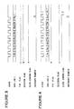
- the T/R flag 46 is set to "0" as shown in Figure 3, so that the AND gates 54 and 56 are put in a closed condition. Therefore, the selector 16 cannot operate.
- the selection flag 44 is set to "1" as shown in Figure 3, with the result that the AND gate 64 is put in a closed condition.
- the AND gate 62 is put in a condition capable of passing its input to the gate of the transistor 28.
- 8-bit parallel data to be transferred is written into the shift register 12 through the data buffer 38 from the internal bus 40.
- a transfer rate data is written into the clock selector 52 so that the selector 52 produces a clock signal of a designated pulse rate from the output of the clock oscillator 70.
- the clock control flag 48 is set to "1" as shown in Figure 3. Further, a signal is supplied to a clear input CL of the counter 78 so as to clear the counter 78, and to the set input S of the flipflop 80 so that the Q output of the flipflop 80 is set to "1".
- the clock signal of the designated pulse rate is supplied from the clock oscillator 70 through the clock selector 52, the NAND gate 72 and the AND gate 74 to the output buffer 76, and then further outputted from the output buffer 76 through the serial clock line 32 to the slave ICs 34 and 36, as shown in Figure 3.
- the clock signal outputted from the output buffer 76 is also supplied to the shift register 12 as the shift clock, so that the shift register 12 performs its shift operation in synchronism with the falling edge of each received shift clock.
- the data serially outputted from the shaft register 12 is applied to the gate of the transistor 28, so that the transistor 28 is turned on or off in accordance with the signal inputted to the gate.
- the data lines 18 and 20 are pulled up to the voltage Vcc through the resistors 22 and 24, respectively, and therefore, a wired logic circuit are formed on each of the data lines. Accordingly, if the transistor 28 is turned off, the data line 18 is pulled up to a high level, and if the transistor 28 is turned on, the data line 18 is pulled down to a low level. In this manner, the serial data is outputted to the data line 18.
- the slave IC 34 fetches the level on the data line 18 in synchronism with the rising edge of each clock signal supplied through the clock line 32.
- the data is serially outputted from the computer 10 (the master station) in synchronism with the falling edge of each clock pulse, and the slave IC 34 fetches the data in synchronism with the rising edge of each clock pulse.
- the counter 78 since the counter 78 is of the three bits, when the counter 78 counts eight clock pulses, the counter 78 generates a carry signal as the interrupt signal, as shown in Figure 3.
- This interrupt signal is supplied to the reset input of the flipflop 80 so that the Q output of the flipflop 80 is brought into "0".
- the NAND gate 72 is closed, and so, the output of the clock pulse is stopped.
- the interrupt signal is also supplied to the CPU 42. In response to this signal, the CPU 42 reads the content of the selection flag 44, and discriminates the destination of the data communication.
- the CPU 42 can start preparation for another data transfer or reception, or can restart a suspended data processing if data communication is not necessary.
- the CPU 42 send through the internal bus 40 various instructions for preparation of data reception.
- the T/R flag 46 is set to "1" as shown in Figure 4 so that the microcomputer is put in a data reception mode.
- the AND gates 62 and 64 are closed, so that the transistors 28 and 30 are maintained off.
- the selection flag 44 is set to "0" as shown in Figure 4, so that the AND gate 54 is put in a closed condition, and only the AND gate 56 is maintained in an open condition, i.e., in a signal passable condition.
- the clock control flag 48 is set to "1" as shown in Figure 4, and a data reception rate is set in the clock selector 52.
- the counter 78 is cleared and the flipflop 80 is set, similarly to the data transmission.
- a clock pulse of a designated pulse rate is supplied from the clock terminal 32A through the clock line 32 to the slace IC 36.
- the slave IC 36 outputs a serial data on the data line 20 one bit by one bit.
- the serial data outputted on the data line 20 is supplied through the AND gate 56 and the OR gate 60 to the serial data input of the shift register 12. This shift register fetches the input data in the rising edge of each shift clock supplied from the output buffer 76.
- the counter 78 When eight clock pulses are generated, the counter 78 generates the carry signal, i.e., the interrupt request signal as shown in Figure 4, which is applied to the reset input of the flipflop 80. Namely, the flipflop 80 is rest, and so, the generation of the clock pulse is stopped. Further, the interrupt request signal is also inputted to the CPU 42. In response to this signal, the CPU 42 reads the content of the selection flag 44, and discriminates the destination of the data communication. In this case, since the selection flag 44 is set with "0", the CPU 42 judges that the destination of the data transmission/reception is the slave IC 36 having a 9-bit format.
- the slave IC 36 In response to the falling of the level on the clock line 32, the slave IC 36 outputs a ninth data bit to the data line 20. Thereafter, the CPU 42 writes "1" to the clock control flag 48 again as shown in Figure 4, so that the output of the AND gate 74 is returned to the high level. Thus, in response to the rising of the level on the clock line 32, the shift register 12 fetches the ninth data bit from the slave IC 36.
- the CPU 42 reads a 9-bit data in the shift register 12 through the data buffer 38, and then, execute necessary data processing.
- the CPU judges from the content of the selection flag 44 that the destination of the data communication is the slave IC 34. In this case, the CPU 42 will not write "0" and "1" to the clock control flag 48.
- the CPU judges from the content of the selection flag 44 that the destination of the data communication is the slave IC 36. In this case, the CPU 42 will sequentially write "0" and "1" to the clock control flag 48, so that a ninth clock pulse is generated from the output buffer 76. Accordingly, a ninth data bit is outputted from the shift register 12 to the data line 20.
- the clock control flag 48 can control a slave IC having a 10-bit serial data transfer format.
- two or more slave ICs can be coupled to the clock line 32 and each of the data lines 18 and 20.
Landscapes
- Engineering & Computer Science (AREA)
- Theoretical Computer Science (AREA)
- Physics & Mathematics (AREA)
- General Engineering & Computer Science (AREA)
- General Physics & Mathematics (AREA)
- Information Transfer Systems (AREA)
- Communication Control (AREA)
Applications Claiming Priority (2)
| Application Number | Priority Date | Filing Date | Title |
|---|---|---|---|
| JP61265153A JPS63118856A (ja) | 1986-11-06 | 1986-11-06 | シリアル・バス・インタフエ−ス回路 |
| JP265153/86 | 1986-11-06 |
Publications (3)
| Publication Number | Publication Date |
|---|---|
| EP0266790A2 true EP0266790A2 (fr) | 1988-05-11 |
| EP0266790A3 EP0266790A3 (fr) | 1991-04-03 |
| EP0266790B1 EP0266790B1 (fr) | 1995-02-22 |
Family
ID=17413364
Family Applications (1)
| Application Number | Title | Priority Date | Filing Date |
|---|---|---|---|
| EP87116418A Expired - Lifetime EP0266790B1 (fr) | 1986-11-06 | 1987-11-06 | Interface pour bus série permettant le transfert des données en formats différents |
Country Status (4)
| Country | Link |
|---|---|
| US (1) | US5025414A (fr) |
| EP (1) | EP0266790B1 (fr) |
| JP (1) | JPS63118856A (fr) |
| DE (1) | DE3751083T2 (fr) |
Cited By (7)
| Publication number | Priority date | Publication date | Assignee | Title |
|---|---|---|---|---|
| EP0434083A2 (fr) * | 1989-12-21 | 1991-06-26 | Kabushiki Kaisha Toshiba | Système et méthode de transmission de données |
| US5146567A (en) * | 1989-08-22 | 1992-09-08 | Acer Incorporated | Keyboard interface |
| EP0529677A1 (fr) * | 1991-08-30 | 1993-03-03 | Nec Corporation | Interface multicanal dans un microordinateur |
| EP0568199A2 (fr) * | 1992-04-30 | 1993-11-03 | Hewlett-Packard Company | Circuits pour le traitement des signaux avec chaînage en série |
| EP0597583A1 (fr) * | 1992-10-09 | 1994-05-18 | Nokia Mobile Phones Ltd. | Bus sériel entre circuits intégrés |
| EP0682303A1 (fr) * | 1994-05-13 | 1995-11-15 | Robert Bosch Gmbh | Dispositif de commande |
| EP0901081A2 (fr) * | 1997-07-08 | 1999-03-10 | Texas Instruments Inc. | Processeur numérique de traitement de signal comprenant des appareils périphériques et des interfaces externes |
Families Citing this family (10)
| Publication number | Priority date | Publication date | Assignee | Title |
|---|---|---|---|---|
| JP2778222B2 (ja) * | 1990-08-15 | 1998-07-23 | 日本電気株式会社 | 半導体集積回路装置 |
| US5428746A (en) * | 1992-03-23 | 1995-06-27 | Zilog, Inc. | Integrated microprocessor unit generating separate memory and input-output device control signals |
| BR9302419A (pt) * | 1992-06-24 | 1994-01-11 | Motorola Inc | Aparelho e processo para fornecer multiplos sinais de saida,e processo para programar o aparelho |
| US5793993A (en) * | 1995-01-26 | 1998-08-11 | General Magic, Inc. | Method for transmitting bus commands and data over two wires of a serial bus |
| KR100370218B1 (ko) * | 2000-10-31 | 2003-01-29 | 삼성전자 주식회사 | 비디오/오디오 처리용 집적회로에 적합한 제어 신호 전송및 수신방법 및 이에 적합한 장치들 |
| US7200767B2 (en) * | 2002-12-27 | 2007-04-03 | Texas Instruments Incorporated | Maintaining synchronization of multiple data channels with a common clock signal |
| JP2008270887A (ja) * | 2007-04-16 | 2008-11-06 | Murata Mach Ltd | シリアル通信方法 |
| US8452908B2 (en) * | 2009-12-29 | 2013-05-28 | Juniper Networks, Inc. | Low latency serial memory interface |
| CN101854259B (zh) * | 2010-06-04 | 2014-03-19 | 中兴通讯股份有限公司 | 一种数据包的计数方法及系统 |
| JP5783802B2 (ja) * | 2011-05-27 | 2015-09-24 | ミネベア株式会社 | モータ駆動装置、集積回路装置、モータ装置、及びモータ駆動システム |
Citations (1)
| Publication number | Priority date | Publication date | Assignee | Title |
|---|---|---|---|---|
| WO1982002102A1 (fr) * | 1980-12-12 | 1982-06-24 | Ncr Co | Topographie de 'puces' pour controleur de communication a circuits integres |
Family Cites Families (10)
| Publication number | Priority date | Publication date | Assignee | Title |
|---|---|---|---|---|
| US4215243A (en) * | 1978-11-17 | 1980-07-29 | Racal-Vadic Inc. | Automatic modem identification system |
| FR2490434B1 (fr) * | 1980-09-12 | 1988-03-18 | Quinquis Jean Paul | Dispositif de resolution des conflits d'acces et d'allocation d'une liaison de type bus interconnectant un ensemble de processeurs non hierarchises |
| US4458308A (en) * | 1980-10-06 | 1984-07-03 | Honeywell Information Systems Inc. | Microprocessor controlled communications controller having a stretched clock cycle |
| US4410962A (en) * | 1981-02-17 | 1983-10-18 | Pitney Bowes Inc. | Mailing system interface interconnecting incompatible communication systems |
| US4493021A (en) * | 1981-04-03 | 1985-01-08 | The United States Of America As Represented By The Administrator Of The National Aeronautics And Space Administration | Multicomputer communication system |
| US4507732A (en) * | 1981-10-05 | 1985-03-26 | Burroughs Corporation | I/O subsystem using slow devices |
| US4567561A (en) * | 1981-12-24 | 1986-01-28 | International Business Machines Corp. | Large scale integration data processor signal transfer mechanism |
| JPS599305U (ja) * | 1982-07-10 | 1984-01-21 | 日本光フアイバ株式会社 | 光フアイバ用カツタ |
| US4613936A (en) * | 1983-02-25 | 1986-09-23 | International Business Machines Corporation | Centralized generation of data transfer acknowledge pulses for microprocessors |
| US4958344A (en) * | 1985-12-18 | 1990-09-18 | Advanced Micro Devices, Inc. | System for transmitting and receiving asynchronous nonhomogeneous variable width parallel data over a synchronous high speed serial transmission media |
-
1986
- 1986-11-06 JP JP61265153A patent/JPS63118856A/ja active Pending
-
1987
- 1987-11-06 DE DE3751083T patent/DE3751083T2/de not_active Expired - Fee Related
- 1987-11-06 US US07/117,738 patent/US5025414A/en not_active Expired - Lifetime
- 1987-11-06 EP EP87116418A patent/EP0266790B1/fr not_active Expired - Lifetime
Patent Citations (1)
| Publication number | Priority date | Publication date | Assignee | Title |
|---|---|---|---|---|
| WO1982002102A1 (fr) * | 1980-12-12 | 1982-06-24 | Ncr Co | Topographie de 'puces' pour controleur de communication a circuits integres |
Non-Patent Citations (1)
| Title |
|---|
| ELECTRONIC DESIGN. HASBROUCK HEIGHTS,NEW JERSEY, US, vol. 32, no. 9, May 1984, pages 355 - 364; M.GALLUP: "On-chip serial interface aids uC system expansion and eases traffic crunch" * |
Cited By (14)
| Publication number | Priority date | Publication date | Assignee | Title |
|---|---|---|---|---|
| US5146567A (en) * | 1989-08-22 | 1992-09-08 | Acer Incorporated | Keyboard interface |
| EP0434083A3 (en) * | 1989-12-21 | 1992-03-04 | Kabushiki Kaisha Toshiba | Data transfer system and method of transferring data |
| EP0434083A2 (fr) * | 1989-12-21 | 1991-06-26 | Kabushiki Kaisha Toshiba | Système et méthode de transmission de données |
| US5381529A (en) * | 1991-08-30 | 1995-01-10 | Nec Corporation | Shift register with dual clock inputs for receiving and sending information between I/O channels and host based on external and internal clock inputs respectively |
| EP0529677A1 (fr) * | 1991-08-30 | 1993-03-03 | Nec Corporation | Interface multicanal dans un microordinateur |
| JPH0573697A (ja) * | 1991-08-30 | 1993-03-26 | Nec Corp | マイクロコンピユータ |
| US5467090A (en) * | 1992-04-30 | 1995-11-14 | Hewlett-Packard Company | Serial processing circuits with serial chaining |
| EP0568199A3 (en) * | 1992-04-30 | 1994-09-21 | Hewlett Packard Co | Signal processing circuits with serial chaining |
| EP0568199A2 (fr) * | 1992-04-30 | 1993-11-03 | Hewlett-Packard Company | Circuits pour le traitement des signaux avec chaînage en série |
| EP0597583A1 (fr) * | 1992-10-09 | 1994-05-18 | Nokia Mobile Phones Ltd. | Bus sériel entre circuits intégrés |
| EP0682303A1 (fr) * | 1994-05-13 | 1995-11-15 | Robert Bosch Gmbh | Dispositif de commande |
| DE4416879B4 (de) * | 1994-05-13 | 2007-04-26 | Robert Bosch Gmbh | Steuergerät mit Mitteln zur Umschaltung zwischen zwei Datenleitungen |
| EP0901081A2 (fr) * | 1997-07-08 | 1999-03-10 | Texas Instruments Inc. | Processeur numérique de traitement de signal comprenant des appareils périphériques et des interfaces externes |
| EP0901081A3 (fr) * | 1997-07-08 | 2000-05-17 | Texas Instruments Inc. | Processeur numérique de traitement de signal comprenant des appareils périphériques et des interfaces externes |
Also Published As
| Publication number | Publication date |
|---|---|
| DE3751083D1 (de) | 1995-03-30 |
| DE3751083T2 (de) | 1995-10-19 |
| JPS63118856A (ja) | 1988-05-23 |
| EP0266790A3 (fr) | 1991-04-03 |
| EP0266790B1 (fr) | 1995-02-22 |
| US5025414A (en) | 1991-06-18 |
Similar Documents
| Publication | Publication Date | Title |
|---|---|---|
| US5025414A (en) | Serial bus interface capable of transferring data in different formats | |
| EP0258873B1 (fr) | Système interface pour bus sériel pour la transmission de données utilisant une ligne à deux fils comme bus d'horloge et bus de données | |
| US4451886A (en) | Bus extender circuitry for data transmission | |
| US5416909A (en) | Input/output controller circuit using a single transceiver to serve multiple input/output ports and method therefor | |
| US4716526A (en) | Multiprocessor system | |
| EP0163305A2 (fr) | Circuit d'entrée/sortie du type CMOS | |
| US5862405A (en) | Peripheral unit selection system having a cascade connection signal line | |
| US5564061A (en) | Reconfigurable architecture for multi-protocol data communications having selection means and a plurality of register sets | |
| US5142556A (en) | Data transfer system and method of transferring data | |
| US5884044A (en) | Dedicated DDC integrable multimode communications cell | |
| US7089467B2 (en) | Asynchronous debug interface | |
| EP0408353B1 (fr) | Circuit intégré à semi-conducteur | |
| US5617433A (en) | Serial data transfer apparatus | |
| JPS6248846B2 (fr) | ||
| JP2003141062A (ja) | Iicバス制御システム | |
| IE59877B1 (en) | Method and apparatus for transferring data between two data processing equipments each driven by an independent clock | |
| US6885217B2 (en) | Data transfer control circuitry including FIFO buffers | |
| US5896514A (en) | Logic implementation of control signals for on-silicon multi-master data transfer bus | |
| JP4931727B2 (ja) | データ通信システム | |
| JPH10207834A (ja) | シリアル入出力回路 | |
| US5539887A (en) | Input buffer circuit for a microprocessor which prevents improper data input | |
| KR100258866B1 (ko) | 피씨아이 버스의 브릿지회로 | |
| US4969161A (en) | Apparatus for inputting and outputting data | |
| JP2786732B2 (ja) | シリアル・パラレル変換回路 | |
| KR940008481B1 (ko) | 제어시스템의 인터럽트 회로 |
Legal Events
| Date | Code | Title | Description |
|---|---|---|---|
| PUAI | Public reference made under article 153(3) epc to a published international application that has entered the european phase |
Free format text: ORIGINAL CODE: 0009012 |
|
| 17P | Request for examination filed |
Effective date: 19871106 |
|
| AK | Designated contracting states |
Kind code of ref document: A2 Designated state(s): DE FR GB |
|
| PUAL | Search report despatched |
Free format text: ORIGINAL CODE: 0009013 |
|
| AK | Designated contracting states |
Kind code of ref document: A3 Designated state(s): DE FR GB |
|
| 17Q | First examination report despatched |
Effective date: 19930215 |
|
| GRAA | (expected) grant |
Free format text: ORIGINAL CODE: 0009210 |
|
| AK | Designated contracting states |
Kind code of ref document: B1 Designated state(s): DE FR GB |
|
| REF | Corresponds to: |
Ref document number: 3751083 Country of ref document: DE Date of ref document: 19950330 |
|
| ET | Fr: translation filed | ||
| PLBE | No opposition filed within time limit |
Free format text: ORIGINAL CODE: 0009261 |
|
| STAA | Information on the status of an ep patent application or granted ep patent |
Free format text: STATUS: NO OPPOSITION FILED WITHIN TIME LIMIT |
|
| 26N | No opposition filed | ||
| REG | Reference to a national code |
Ref country code: GB Ref legal event code: IF02 |
|
| PGFP | Annual fee paid to national office [announced via postgrant information from national office to epo] |
Ref country code: GB Payment date: 20021106 Year of fee payment: 16 |
|
| PGFP | Annual fee paid to national office [announced via postgrant information from national office to epo] |
Ref country code: DE Payment date: 20021107 Year of fee payment: 16 |
|
| PGFP | Annual fee paid to national office [announced via postgrant information from national office to epo] |
Ref country code: FR Payment date: 20021108 Year of fee payment: 16 |
|
| REG | Reference to a national code |
Ref country code: GB Ref legal event code: 732E |
|
| REG | Reference to a national code |
Ref country code: FR Ref legal event code: TP |
|
| PG25 | Lapsed in a contracting state [announced via postgrant information from national office to epo] |
Ref country code: GB Free format text: LAPSE BECAUSE OF NON-PAYMENT OF DUE FEES Effective date: 20031106 |
|
| PG25 | Lapsed in a contracting state [announced via postgrant information from national office to epo] |
Ref country code: DE Free format text: LAPSE BECAUSE OF NON-PAYMENT OF DUE FEES Effective date: 20040602 |
|
| GBPC | Gb: european patent ceased through non-payment of renewal fee |
Effective date: 20031106 |
|
| PG25 | Lapsed in a contracting state [announced via postgrant information from national office to epo] |
Ref country code: FR Free format text: LAPSE BECAUSE OF NON-PAYMENT OF DUE FEES Effective date: 20040730 |
|
| REG | Reference to a national code |
Ref country code: FR Ref legal event code: ST |