EP0263756B1 - Verwendung einer selektiven Epitaxie für BiCMOS-Verfahren - Google Patents
Verwendung einer selektiven Epitaxie für BiCMOS-Verfahren Download PDFInfo
- Publication number
- EP0263756B1 EP0263756B1 EP87402208A EP87402208A EP0263756B1 EP 0263756 B1 EP0263756 B1 EP 0263756B1 EP 87402208 A EP87402208 A EP 87402208A EP 87402208 A EP87402208 A EP 87402208A EP 0263756 B1 EP0263756 B1 EP 0263756B1
- Authority
- EP
- European Patent Office
- Prior art keywords
- regions
- layer
- epitaxial layer
- forming
- silicon
- Prior art date
- Legal status (The legal status is an assumption and is not a legal conclusion. Google has not performed a legal analysis and makes no representation as to the accuracy of the status listed.)
- Expired - Lifetime
Links
Images

Classifications
-
- H—ELECTRICITY
- H10—SEMICONDUCTOR DEVICES; ELECTRIC SOLID-STATE DEVICES NOT OTHERWISE PROVIDED FOR
- H10D—INORGANIC ELECTRIC SEMICONDUCTOR DEVICES
- H10D1/00—Resistors, capacitors or inductors
- H10D1/40—Resistors
- H10D1/47—Resistors having no potential barriers
-
- H—ELECTRICITY
- H10—SEMICONDUCTOR DEVICES; ELECTRIC SOLID-STATE DEVICES NOT OTHERWISE PROVIDED FOR
- H10D—INORGANIC ELECTRIC SEMICONDUCTOR DEVICES
- H10D84/00—Integrated devices formed in or on semiconductor substrates that comprise only semiconducting layers, e.g. on Si wafers or on GaAs-on-Si wafers
- H10D84/01—Manufacture or treatment
- H10D84/0107—Integrating at least one component covered by H10D12/00 or H10D30/00 with at least one component covered by H10D8/00, H10D10/00 or H10D18/00, e.g. integrating IGFETs with BJTs
- H10D84/0109—Integrating at least one component covered by H10D12/00 or H10D30/00 with at least one component covered by H10D8/00, H10D10/00 or H10D18/00, e.g. integrating IGFETs with BJTs the at least one component covered by H10D12/00 or H10D30/00 being a MOS device
-
- H—ELECTRICITY
- H10—SEMICONDUCTOR DEVICES; ELECTRIC SOLID-STATE DEVICES NOT OTHERWISE PROVIDED FOR
- H10D—INORGANIC ELECTRIC SEMICONDUCTOR DEVICES
- H10D64/00—Electrodes of devices having potential barriers
- H10D64/01—Manufacture or treatment
- H10D64/021—Manufacture or treatment using multiple gate spacer layers, e.g. bilayered sidewall spacers
-
- H—ELECTRICITY
- H10—SEMICONDUCTOR DEVICES; ELECTRIC SOLID-STATE DEVICES NOT OTHERWISE PROVIDED FOR
- H10D—INORGANIC ELECTRIC SEMICONDUCTOR DEVICES
- H10D84/00—Integrated devices formed in or on semiconductor substrates that comprise only semiconducting layers, e.g. on Si wafers or on GaAs-on-Si wafers
- H10D84/01—Manufacture or treatment
- H10D84/0123—Integrating together multiple components covered by H10D12/00 or H10D30/00, e.g. integrating multiple IGBTs
- H10D84/0126—Integrating together multiple components covered by H10D12/00 or H10D30/00, e.g. integrating multiple IGBTs the components including insulated gates, e.g. IGFETs
- H10D84/0165—Integrating together multiple components covered by H10D12/00 or H10D30/00, e.g. integrating multiple IGBTs the components including insulated gates, e.g. IGFETs the components including complementary IGFETs, e.g. CMOS devices
-
- H—ELECTRICITY
- H10—SEMICONDUCTOR DEVICES; ELECTRIC SOLID-STATE DEVICES NOT OTHERWISE PROVIDED FOR
- H10D—INORGANIC ELECTRIC SEMICONDUCTOR DEVICES
- H10D84/00—Integrated devices formed in or on semiconductor substrates that comprise only semiconducting layers, e.g. on Si wafers or on GaAs-on-Si wafers
- H10D84/01—Manufacture or treatment
- H10D84/02—Manufacture or treatment characterised by using material-based technologies
- H10D84/03—Manufacture or treatment characterised by using material-based technologies using Group IV technology, e.g. silicon technology or silicon-carbide [SiC] technology
- H10D84/038—Manufacture or treatment characterised by using material-based technologies using Group IV technology, e.g. silicon technology or silicon-carbide [SiC] technology using silicon technology, e.g. SiGe
-
- H—ELECTRICITY
- H10—SEMICONDUCTOR DEVICES; ELECTRIC SOLID-STATE DEVICES NOT OTHERWISE PROVIDED FOR
- H10D—INORGANIC ELECTRIC SEMICONDUCTOR DEVICES
- H10D84/00—Integrated devices formed in or on semiconductor substrates that comprise only semiconducting layers, e.g. on Si wafers or on GaAs-on-Si wafers
- H10D84/80—Integrated devices formed in or on semiconductor substrates that comprise only semiconducting layers, e.g. on Si wafers or on GaAs-on-Si wafers characterised by the integration of at least one component covered by groups H10D12/00 or H10D30/00, e.g. integration of IGFETs
- H10D84/82—Integrated devices formed in or on semiconductor substrates that comprise only semiconducting layers, e.g. on Si wafers or on GaAs-on-Si wafers characterised by the integration of at least one component covered by groups H10D12/00 or H10D30/00, e.g. integration of IGFETs of only field-effect components
- H10D84/83—Integrated devices formed in or on semiconductor substrates that comprise only semiconducting layers, e.g. on Si wafers or on GaAs-on-Si wafers characterised by the integration of at least one component covered by groups H10D12/00 or H10D30/00, e.g. integration of IGFETs of only field-effect components of only insulated-gate FETs [IGFET]
- H10D84/85—Complementary IGFETs, e.g. CMOS
-
- H—ELECTRICITY
- H10—SEMICONDUCTOR DEVICES; ELECTRIC SOLID-STATE DEVICES NOT OTHERWISE PROVIDED FOR
- H10P—GENERIC PROCESSES OR APPARATUS FOR THE MANUFACTURE OR TREATMENT OF DEVICES COVERED BY CLASS H10
- H10P14/00—Formation of materials, e.g. in the shape of layers or pillars
- H10P14/60—Formation of materials, e.g. in the shape of layers or pillars of insulating materials
- H10P14/63—Formation of materials, e.g. in the shape of layers or pillars of insulating materials characterised by the formation processes
- H10P14/6326—Deposition processes
- H10P14/6349—Deposition of epitaxial materials
-
- H—ELECTRICITY
- H10—SEMICONDUCTOR DEVICES; ELECTRIC SOLID-STATE DEVICES NOT OTHERWISE PROVIDED FOR
- H10P—GENERIC PROCESSES OR APPARATUS FOR THE MANUFACTURE OR TREATMENT OF DEVICES COVERED BY CLASS H10
- H10P32/00—Diffusion of dopants within, into or out of wafers, substrates or parts of devices
- H10P32/30—Diffusion for doping of conductive or resistive layers
- H10P32/302—Doping polycrystalline silicon or amorphous silicon layers
-
- H—ELECTRICITY
- H10—SEMICONDUCTOR DEVICES; ELECTRIC SOLID-STATE DEVICES NOT OTHERWISE PROVIDED FOR
- H10P—GENERIC PROCESSES OR APPARATUS FOR THE MANUFACTURE OR TREATMENT OF DEVICES COVERED BY CLASS H10
- H10P50/00—Etching of wafers, substrates or parts of devices
- H10P50/20—Dry etching; Plasma etching; Reactive-ion etching
- H10P50/24—Dry etching; Plasma etching; Reactive-ion etching of semiconductor materials
- H10P50/242—Dry etching; Plasma etching; Reactive-ion etching of semiconductor materials of Group IV materials
-
- H—ELECTRICITY
- H10—SEMICONDUCTOR DEVICES; ELECTRIC SOLID-STATE DEVICES NOT OTHERWISE PROVIDED FOR
- H10W—GENERIC PACKAGES, INTERCONNECTIONS, CONNECTORS OR OTHER CONSTRUCTIONAL DETAILS OF DEVICES COVERED BY CLASS H10
- H10W10/00—Isolation regions in semiconductor bodies between components of integrated devices
- H10W10/01—Manufacture or treatment
- H10W10/011—Manufacture or treatment of isolation regions comprising dielectric materials
- H10W10/018—Manufacture or treatment of isolation regions comprising dielectric materials using selective deposition of crystalline silicon, e.g. using epitaxial growth of silicon
-
- H—ELECTRICITY
- H10—SEMICONDUCTOR DEVICES; ELECTRIC SOLID-STATE DEVICES NOT OTHERWISE PROVIDED FOR
- H10W—GENERIC PACKAGES, INTERCONNECTIONS, CONNECTORS OR OTHER CONSTRUCTIONAL DETAILS OF DEVICES COVERED BY CLASS H10
- H10W10/00—Isolation regions in semiconductor bodies between components of integrated devices
- H10W10/10—Isolation regions comprising dielectric materials
Definitions
- This invention relates to processes for fabricating integrated circuits, and to processes for fabricating both bipolar and complementary field effect transistors in the same substrate.
- the invention relates to a BiCMOS process in which selective formation of an epitaxial layer is employed to isolate individual bipolar and CMOS transistors, as well as other components.
- Bipolar and CMOS technologies have each been independently understood for many years. Recently, however, the ability to combine CMOS with bipolar on the same integrated circuit has raised new possibilities for very large scale integration. For example, bipolar output drivers may be employed with CMOS memories to provide more drive current. Because normally MOS circuits operate slower with increasing temperature, while bipolar operates faster, a CMOS bipolar combination may be employed to make devices less speed sensitive to temperature. In addition, combining high performance bipolar devices with MOS transistors on the same integrated circuit allows a combination of the high-packing density of MOS devices and permits the ability to integrate complex functions with high yields. The CMOS circuits have inherently low power requirements, while the bipolar devices have an advantage in switching speed and current drive per unit area.
- CMOS process provides little for the ad hoc bipolar devices as they end up being built from CMOS spare parts and display lackluster performance.
- CMOS spare parts and display lackluster performance As a result, the compromised technology cannot compete on its own against processes optimized for either of the constituent bipolar or CMOS devices.
- Typical prior art bipolar-CMOS processes may be found in U.S. Patent 4,484,388 to Iwasaki; U.S. Patent 4,507,847 to Sullivan; and U.S. Patent 4,536,945 to Gray et al. ; and U.S. Patent 3,955,269 to Magdo et al.
- Patent Abstracts of Japan, vol. 6, no. 16, (E92) ⁇ 894> Jan. 29, 1982 & JP-A-56 137 647 relates to the fabrication of bipolar devices and teaches a method of providing grooves which extend through an epitaxial layer to a p-type substrate, the sidewalls of the grooves being then oxidized, and the grooves filled with another epitaxial layer so as to separate individual devices from one another.
- EP-A-0 155 698 teaches forming of grooves in a main surface of the semiconductor substrate and oxidizing the sidewalls of the islands so formed. The grooves are then filled with crystalline semiconductor material, and devices may be formed in the islands and/or the groove filler.
- EP-A-0 097 379 teaches a method of simultaneous formation of bipolar and CMOS devices on a common substrate wherein the base region of an npn transistor and the source and drain regions of a p channel MOS device are formed simultaneously, and the collector region of the npn transistor and source and drain regions of a n channel MOS device are then also formed simultaneously.
- the BiCMOS process of my invention provides high performance bipolar and CMOS devices. By employing selective epitaxy, self-aligned complementary silicon regions are formed, thereby reducing mask count. Furthermore, the process strongly decouples the bipolar and CMOS devices.
- the determination of whether a given silicon island in my process will become a bipolar device or an MOS device is determined by a technology mask.
- the technology mask consists of a mask which determines whether previously-formed gate oxide is etched away or allowed to remain in place. When the gate oxide is etched away, a subsequent layer of polycrystalline silicon directly contacts the epitaxial layer to form the bipolar emitter contact. When the gate oxide is not removed, the subsequent polycrystalline silicon forms the gate electrode of the field effect device.
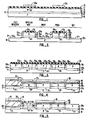
- Figure 1 is a cross-sectional view of a semiconductor structure fabricated using well known process operations beginning with a wafer 10.
- a blanket implant of a buried layer 12 is made into the P conductivity type silicon substrate 10.
- the resistivity of the substrate is on the order of 10-20 ohm centimeters, while the buried layer is implanted with arsenic with a concentration of approximately 3-5x10¹⁵ atoms per square centimeter.
- the structure is annealed, for example, at 1100°C for 60 minutes.
- an epitaxial layer 15 is formed using a conventional process. Epitaxial layer 15 is doped lightly with N conductivity type impurity and is about 1.2 microns »m thick.
- the conductivity types of the enumerated regions 10, 12, and 15, may be reversed.
- the described process is preferred because of the difficulty of controlling P conductivity type impurity diffusions during the formation of the epitaxial layer (and its reformation described below).
- the regions of nitride to be removed correspond to the regions of the epitaxial layer to be removed, primarily the locations of the NMOS devices, but also the locations for polysilicon resistors and substrate taps.
- silicon nitride layer 19 is removed except where protected by the mask 20.
- the underlying and thereby exposed regions of silicon dioxide 17 are removed. Because layers 17, 19 are relatively thin, either wet or dry (plasma) processes may be employed to remove them.
- the etching process is continued to remove all of the thereby exposed epitaxial layer 15 and underlying buried layer 12.
- the interface of buried layer 12 with substrate 10 is approximately 2 microns beneath the surface of substrate 10, assuming a 1.2-micron-thick epitaxial layer 15.
- the removal of the epitaxial layer 15 and buried layer 12 is preferably accomplished using an anisotropic etching process. In this manner an essentially vertical cut is made through the layers with minimal lateral etching beneath the protective silicon nitride caps 19a and 19b. As a result of this process, regions of the epitaxial layer and buried layer having sidewalls 21 protrude above the substrate 10.
- the reactive ion etch of the silicon 15, 12 and 10 is allowed to remove approximately 2.5 microns of silicon beneath the upper surface of the epitaxial layer 15. Viewed from the top, the resulting islands will be rectangular (usually) with width and height of appropriate dimension for the formation of a transistor.
- the structure is next oxidized by heating it in steam to approximately 1000°C for 70 minutes. This process forms about 5,000 Angstroms of silicon dioxide over the exposed upper surface of substrate 10 and over the sidewalls 21 of the protruding islands of buried layer 12 and epitaxial layer 15.
- silicon dioxide layer 25 may be applied using a low temperature process such as chemical vapor deposition.
- Reactive ion-etching is then used to remove the silicon dioxide from the surface of substrate 10.
- silicon dioxide is removed from this surface without significantly removing it from the sidewalls 21 of the protruding silicon regions 12 and 15.
- a P conductivity type implant also masked by the nitride 19 and oxide 25, provides a buried layer 22.
- the implant is annealed for about 60 minutes at 950°C. Buried layer 22 destroys any lateral current path from one region of the epitaxial silicon to an adjoining region.
- the buried layer guarantees that any parasitic bipolar transistor formed by the source/drain (parasitic emitter) through the epitaxial layer (parasitic base) to an adjacent well will have a very low beta. Such a buried layer thus effectively suppresses latchup in the CMOS structures to be formed by later process operations.
- FIG. 2 The appearance of the structure following implanting of regions 22 is shown in Figure 2. Across the upper portion of Figure 2, regions of the structure are labeled to describe the component which will be formed therein. For example, from left to right in the middle of the structure, an NPN bipolar transistor will be formed adjacent an N channel MOS transistor, in turn adjacent a P channel MOS transistor. A substrate tap will be formed at the right side of the structure, while the resistor will be formed at the left side.
- the structure shown in Figure 2 then is introduced into an epitaxial reactor, and a further layer of epitaxial silicon 28 deposited (see Figure 3).
- the silicon dioxide protective layers 17 and 25 prevent epitaxial silicon from forming upon the upper surface of the protruding regions.
- the upper surface of the new epitaxial regions 28 will be substantially planar with the upper surface of the previously-formed epitaxial regions 15.
- the silicon nitride 19 and silicon dioxide 17 are removed from the surface of the structure using conventional etchants.
- a sacrificial oxidation may be employed by which the upper surface is oxidized, and the resulting silicon dioxide removed, also using the conventional etching technology.
- a new layer of silicon dioxide 30 approximately 250 Angstroms thick then is formed by heating the structure to a temperature of 1000°C for 20 minutes. Then another layer of silicon nitride 32 approximately 1100 Angstroms thick is deposited on silicon dioxide 30, using conventional chemical vapor deposition.
- the P conductivity type regions 22 will diffuse outward, thereby extending upward into the epitaxial layer 28.
- the newly-formed regions of epitaxial silicon 28a, 28b, and 28c will be lightly doped with P conductivity type impurity, for example, boron, and will have an impurity concentration on the order of 1x10¹⁷ atoms per cubic centimeter.
- nitride 32 is formed across the upper surface of nitride 32 to define those regions where field oxide is desired.
- the field oxide is formed wherever a polysilicon resistor is desired.
- the mask is removed from the surface of the structure above epitaxial region 28a, and allowed to remain everywhere else. Again, using conventional etching technology, the exposed portions of silicon nitride 32 and silicon dioxide 30 are removed.
- a channel stop 29 may be implanted, if desired. The channel stop 29 prevents the formation of parasitic N channels beneath the silicon dioxide isolation regions.
- boron is implanted with a dose of 1x10¹³ atoms per square centimeter at 50 KeV using the resist as a mask.
- the implant is annealed at about 900°C for 30 minutes.
- the structure then is oxidized in steam at a temperature of 1000°C for about 70 minutes to form approximately 5,000 Angstroms of field oxidation 35 (shown in Figure 4).
- the field oxide 35 will decouple the later-formed overlying polysilicon resistor from the epitaxial region 28a.
- Field oxide 35 will also provide insulation for overlying electrical connections. Use of the relatively thick oxide 35 in this manner avoids possible shorts to the epitaxial layer which occur when thinner oxide is employed. Furthermore, the thick oxide 35 decouples such conducting lines from the substrate.
- silicon dioxide 38 typically is about 200 Angstroms thick and formed by heating the structure to a temperature of 950°C for 20 minutes in an oxidizing ambient. The gate oxide will separate the gate electrodes of the MOS devices from the epitaxial layer.
- gate oxide 38 in the preferred embodiment a thin (about 500 Angstroms) layer of polycrystalline silicon may be deposited. This is optional to my process, because if desired all of the polysilicon may be deposited later. If employed, the polysilicon protects the gate oxide from subsequently formed photoresist, patterning, and annealing. Then a mask 39 is formed across the upper surface of the structure and openings are provided, using well known photolithographic techniques, wherever a contact (collector sink) to the buried collector of a bipolar device is desired. One such opening in the mask 39 over region 15a is illustrated.
- a high energy implant of N conductivity type impurity typically phosphorus, then defines a collector sink 40.
- the implant has a dosage of approximately 2x10¹⁵ atoms per square centimeter and an energy of 180 KeV.
- Mask 39 protects the remainder of the silicon. The mask is then stripped and the collector sink annealed for about 60 minutes at about 1000°C.
- a "technology" mask 41 is defined across the upper surface of the structure. As shown in Figure 5, openings are made in the mask 41 wherever bipolar devices are desired, for example, above all of epitaxial region 15a. Additionally, in the preferred embodiment of my process, openings are made in mask 41 wherever substrate taps are desired, e.g., above epitaxial region 28c.
- the exposed regions of the thin layer of polysilicon 45 are then etched away using well known processes.
- the thereby exposed gate oxide 38 is allowed to remain on the surface of the epitaxial layer.
- the intrinsic base 42 of the bipolar transistor then is implanted through the gate oxide with P conductivity type impurity.
- a concentration of 1x10¹³ atoms per square centimeter of boron are employed at an energy of 40 KeV.
- the base implant also dopes the substrate tap more P-type.
- the exposed gate oxide 38 is then etched off using a suitable wet etch and the structure then is annealed by heating it to a temperature of 900°C for 30 minutes to repair any dislocations caused by the collector sink and the base implantations. During this process the gate oxide beneath resist 41 will not grow thicker.
- polysilicon 45 is 4500 Angstroms thick and is deposited using chemical vapor deposition.
- the structure then is heated in an oxygen ambient to form silicon dioxide 47 across the upper surface of polycrystalline silicon 45. Silicon dioxide 47 will be of the order of 200 to 400 Angstroms thick.
- approximately 1,500 Angstroms of silicon nitride 50 are deposited across the upper surface of silicon dioxide 47.
- silicon nitride is defined into regions 50a-50f as shown in Figure 6.
- the silicon dioxide 47 provides an etch stop for the removal of the undesired silicon nitride.
- the silicon nitride not only protects the polycrystalline silicon from a subsequent implant which defines the gates and emitter regions, but also protects the polysilicon 45 from oxidation in a subsequent process step.
- a strong implant of N conductivity type impurity typically 1x10¹⁶ atoms per square centimeter of arsenic, dopes the unprotected regions of the polysilicon 45.
- the strongly doped regions provide a resistor contact 46a, an emitter contact 46b, a collector sink contact 46c, an N channel gate electrode 46d, and a P channel gate electrode 46e.
- This small region acts as a spacer and prevents the extrinsic base dopant from being placed next to the collector sink, which would create a structure with a low breakdown voltage and a high capacitance PN junction where the extrinsic base would otherwise join the collector sink.
- Another mask then is formed across the upper surface of the structure to protect the structure except where sources and drains of the NMOS device are desired, i.e., not overlying region 28b of the epitaxial layer.
- a heavy N conductivity type implant then creates source/drain regions 53a, 53b.
- the impurity comprises arsenic and is implanted to a concentration of 5x10¹⁵ atoms per square centimeter with an energy of 100 KeV.
- the structure then is annealed by heating it to a temperature of 950°C for 30 minutes. During this annealing N-type impurity in the emitter contact 46b diffuses out of the contact and into the epitaxial layer 42 to dope the emitter region 64.
- the N type implant will be lighter than the normal dose, with a heavier dose applied later in the process, for example, as described in conjunction with Figure 9.
- a double implant may be employed with two impurities having different diffusivities, for example, phosphorus and arsenic. The phosphorus will diffuse into the structure ahead of the arsenic, thereby forming a lightly doped drain structure.
- a layer of silicon dioxide 57 forms over the exposed polycrystalline silicon. Because N conductivity type silicon oxidize faster than P type, the layer of silicon dioxide 57 is thicker over the N type regions than over the P type regions. Thus, silicon dioxide region 57b is thicker over the N type polysilicon emitter contact 46b than over the underlying extrinsic base 42.
- the P type dopant is boron implanted with 3x10¹⁵ atoms per square centimeter at an energy of about 30 KeV. This is sufficient to penetrate the thin oxide 38 but not the thicker oxide 57.
- a relatively thick layer of silicon dioxide then is deposited across the upper surface of the structure shown in Figure 8 and anisotropically etched to form the spacer oxide regions 60a-60f shown in Figure 9.
- the reactive ion etch may be performed using an end point detector.
- the structure may be dipped in hydrofluoric acid. If lightly doped drain structures are desired, an additional mask is formed across the surface of the semiconductor structure to expose only the NMOS devices. This mask, together with the spacer oxide 60c and 60d, will mask an additional implant of N type impurity to heavily dope the regions of the NMOS source and drain spaced apart from the gate.
- a layer of silicide-forming metal is deposited across the entire upper surface of the structure and reacted with the underlying silicon.
- regions of metal silicide 62 are formed across the upper surface of the structure as shown in Figure 9.
- the metal comprises titanium, and the step of reacting it with the silicon consists of heating the structure to a temperature of 800°C in a neutral ambient for about 15 minutes.
- the silicon nitride regions 50a and 50c prevent the silicide from shorting the polysilicon resistor formed on field oxide 35 and from shorting the collector contact 46c to the extrinsic base 59b.
- the structure is masked to define local interconnections between the various component parts, and any unreacted titanium is removed using ammonium hydroxide and hydrogen peroxide etchants.
- silicide region 62a connects one electrode 46a of resistor 45a to the base 59a of the NPN transistor.
- Silicide 62b connects to the emitter 65 which is formed by N-type impurity diffusing out of polysilicon region 46b during the formation of titanium silicide.
- Another region of titanium silicide 62c lowers the resistance of the extrinsic base.
- Silicide 62e is a connection to one of the source/drain of the NMOS device, while silicide 62g shorts the other of the source/drain to one of the source/drain of the PMOS device.
- Metal silicide 62f provides a low resistance connection to the gate of the NMOS device, while silicide region 62h provides a similar connection to the gate of the PMOS device.
- One of the source/drain of the PMOS device is shorted to the substrate by silicide 62i.
- silicon dioxide 65 is deposited across the surface as shown in Figure 10. Silicon dioxide 65 is masked and regions of silicon dioxide 65 are removed wherever electrical connections to the underlying silicide are desired. The resulting structure is shown in Figure 10 before formation of such metal connections.
- metal silicide as a local interconnection allows the formation of very small source/drain regions and extrinsic base regions to which electrical connections may be made on field oxide.
- the process described above results in the fabrication of bipolar transistors having very low parasitic capacitance.
- the collectors of the bipolar devices are fully isolated on their periphery by silicon dioxide which reduces the capacitance between the collector and the substrate. This is a substantial advantage over existing processes in which the lateral component of the collector-substrate capacitance dominates over the vertical component for minimum geometry transistors.
- the self-aligned local interconnection system formed by the metal silicide allows base area to be minimized, thereby reducing base-collector capacitance.
- the low capacitance allows high switching frequencies.
- the employment of selective oxidation i.e., reliance upon the different oxidation rates of N and P type silicon, minimizes masking operations. Because buried layers are provided under both the N and P channel transistors, there is no lateral current path available, thereby minimizing latchup.
- the silicide source/drain regions lower contact resistance and minimize area by allowing remote connections to the field effect devices, thereby improving performance.
- the doping of the P epitaxial layer is effectively decoupled from other process considerations, it may be optimized to suit the desired performance of the N channel devices. In essence, the performance of each of the bipolar and CMOS devices may be appropriately controlled to obtain maximum performance from each without compromising either to suit the fabrication of the other.
Landscapes
- Metal-Oxide And Bipolar Metal-Oxide Semiconductor Integrated Circuits (AREA)
- Bipolar Transistors (AREA)
Claims (23)
- Ein Verfahren für die Herstellung von sowohl bipolaren als auch Feldeffekttransistoren in einer Struktur, umfassend in Aufeinanderfolge die Schritte:
Bereitstellen einer Struktur mit einem Halbleitersubstrat (10) eines ersten Leitfähigkeitstyps, einer Epitaxialschicht (15) zweiten Leitfähigkeitstyps und einer vergrabenen Schicht (12) des zweiten Leitfähigkeitstyps, welche das Substrat von der Epitaxialschicht trennt;
Abtragen der gesamten Epitaxialschicht und der gesamten vergrabenen Schicht von ersten Bereichen, wo Feldeffekttransistoren ersten Kanaltyps gewünscht werden, um dadurch zweite Bereiche der Epitaxialschicht und der vergrabenen Schicht in Form von Inseln (15a, 15b) zu belassen, welche über die Substratoberfläche hinausragen und Seitenwandungen (21) aufweisen,
Bilden einer Schicht aus Isoliermaterial (25a-d) über den Seitenwandungen der zweiten Bereiche,
Aufbringen von Halbleitermaterial (28a-c) über den ersten Bereichen, um dadurch die Epitaxialschicht über den ersten Bereichen zu reformieren, wobei die Epitaxialschicht in den zweiten Bereichen von der Epitaxialschicht in den ersten Bereichen durch das isolierende Material getrennt ist; und
Bilden von Feldeffekt- und bipolaren Transistoren in dem ersten bzw. zweiten Bereich. - Ein Verfahren nach Anspruch 1, bei dem der Schritt des Abtrags der gesamten Epitaxialschicht und der gesamten vergrabenen Schicht aus den ersten Bereichen umfaßt:
Maskieren der zweiten Bereiche der Epitaxialschicht mit einem ätzfesten Material (20); und
Ätzen der Epitaxialschicht und der vergrabenen Schicht zum Freilegen des Substrats in den ersten Bereichen. - Ein Verfahren nach Anspruch 2, bei dem der Schritt des Ätzens reaktives Ionenätzen umfaßt.
- Ein Verfahren nach Anspruch 2, bei dem der Schritt des Maskierens der Epitaxialschicht das Bilden einer ersten Schicht (17) aus Siliciumdioxid auf der Epitaxialschicht und einer Schicht (19) aus Siliciumnitrid auf dem Siliciumdioxid umfaßt.
- Ein Verfahren nach Anspruch 4, bei dem sowohl das Substrat (10) als auch die Epitaxialschicht (15) Silicium umfaßt.
- Ein Verfahren nach Anspruch 5, bei dem der Schritt der Bildung einer Schicht aus isolierendem Material über den Seitenwandungen das Oxidieren der Seitenwandungen der zweiten Bereiche zur Bildung von Siliciumdioxid umfaßt.
- Ein Verfahren nach Anspruch 6, bei dem der Schritt der Bildung einer Schicht aus Isoliermaterial außerdem das Oxidieren der freiliegenden oberen Oberfläche des Substrats in den ersten Bereichen umfaßt und ihm ein Schritt des Ätzens des Isoliermaterials von den ersten Bereichen ausgenommen an einer Peripherie derselben folgt.
- Ein Verfahren nach Anspruch 7, bei dem dem Schritt des Ätzens des Isoliermaterials von den ersten Bereichen ein Schritt des Implantierens von Dotierungsmittel ersten Leitfähigkeitstyps in die ersten Bereiche folgt und zweite Bereiche geschützt werden durch die Schicht aus Siliciumnitrid.
- Ein Verfahren nach Anspruch 5, bei dem der Schritt der Bildung einer Schicht aus Isoliermaterial das Aufbringen von Siliciumdioxid unter Anwendung von chemischem Dampfniederschlag umfaßt.
- Ein Verfahren nach Anspruch 1, bei dem der Schritt der Bildung bipolarer und Feldeffekttransistoren das Oxidieren der Epitaxialschicht in sowohl den ersten als auch den zweiten Bereichen zur Bildung einer Schicht von Gate-Oxid (38) umfaßt.
- Ein Verfahren nach Anspruch 10, bei dem dem Schritt des Oxidierens der Epitaxialschicht ein Schritt der Definition von polykristallinen Silicium-Gate-Elektroden (45) auf dem Gate-Oxid folgt.
- Ein Verfahren nach Anspruch 11, bei dem dem Schritt der Definition der polykristallinen Silicium-Gate-Elektroden ein Schritt der Verwendung der polykristallinen Silicium-Gate-Elektroden als eine Maske für das Implantieren von Sources and Drains der Feldeffekttransistoren folgt.
- Ein Verfahren nach Anspruch 12, bei dem dem Schritt der Verwendung der polykristallinen Silicium-Gate-Elektroden als Maske ein Schritt der Bildung von Silicium-Dioxid (47)-Distanzregionen (60) auf Seiten der Gate-Elektroden ausgeführt wird.
- Ein Verfahren nach Anspruch 13, bei dem dem Schritt der Bildung der Distanzbereiche ein Schritt des Auftrags von Silicid bildendem Metall auf die Struktur folgt.
- Ein Verfahren nach Anspruch 13, bei dem der Schritt der Bildung von Siliciumdioxid-Distanzbereichen umfaßt:
Oxidieren der Halbleiterstruktur; und
anisotropes Ätzen der Struktur zum Abtrag des dadurch gebildeten Siliciumdioxid von der Struktur ausgenommen von den Distanzbereichen. - Ein Verfahren nach Anspruch 1, bei dem der Schritt der Bildung bipolarer und Feldeffekttransistoren die Bildung einer Kollektorsenke (40) umfaßt, die sich zu der vergrabenen Schicht in einem zweiten Bereich erstreckt.
- Ein Verfahren nach Anspruch 16, bei dem dem Schritt der Bildung einer Kollektorsenke ein Schritt des Implantierens eines Basisbereichs (42) des bipolaren Transistors in den zweiten Bereich folgt.
- Ein Verfahren nach Anspruch 17, bei dem dem Schritt des Implantierens eines Basisbereichs ein Schritt der Definition eines polykristillinen Silicium-Emitterkontakts (46b) für den Bipolartransistor folgt.
- Ein Verfahren nach Anspruch 1, bei dem der Schritt der Bildung bipolarer und Feldeffekttransistoren ferner die Bildung von Widerständen umfaßt.
- Ein Verfahren nach Anspruch 19, bei dem der Schritt der Bildung von Widerständen das Oxidieren eines der ersten und zweiten Bereiche zur Bildung eines Feldoxidbereichs umfaßt.
- Ein Verfahren nach Anspruch 20, bei dem dem Schritt der Oxidierung eines der ersten oder zweiten Bereiche der Schritt des Aufbringens von polykristallinem Silicium auf den Feldoxidbereich folgt.
- Ein Verfahren nach Anspruch 21, bei dem dem Schritt des Aufbringens von polykristallinem Silicium auf das Feldoxid ein Schritt des Schützens eines Bereiches des polykristallinen Siliciums, das zu einem Widerstand werden soll, und das Einführen von Dotierungsmitteln in zwei beabstandete Bereiche des polykristallinen Siliciums folgt, um dadurch elektrische Verbindungen zu dem Widerstand zu bilden.
- Das Verfahren nach Anspruch 8, bei dem das Substrat (10) ein Siliciumsubstrat vom P-Leitfähigkeitstyp ist, während die epitaxiale (15) und vergrabene Schicht (12) vom N-Leitfähigkeitstyp sind, bei welchem
P-Dotierungsmittel in das Substrat in den ersten Bereichen implantiert wird zur Bildung einer P-leitenden vergrabenen Schicht in den ersten Bereichen und
Silicium (28) über zumindest den ersten Bereichen aufgebracht wird, um dadurch die Epitaxialschicht über den ersten Bereichen zu reformieren, wobei die Epitaxialschicht in den zweiten Bereichen von der Epitaxialschicht in den ersten Bereichen durch Siliciumdioxid (25) getrennt ist, und bei dem
bipolare Transistoren in den zweiten Bereichen gebildet werden und Feldeffekttransistoren in jedem der ersten und zweiten Bereiche.
Applications Claiming Priority (2)
| Application Number | Priority Date | Filing Date | Title |
|---|---|---|---|
| US91545086A | 1986-10-06 | 1986-10-06 | |
| US915450 | 1986-10-06 |
Publications (3)
| Publication Number | Publication Date |
|---|---|
| EP0263756A2 EP0263756A2 (de) | 1988-04-13 |
| EP0263756A3 EP0263756A3 (en) | 1989-09-06 |
| EP0263756B1 true EP0263756B1 (de) | 1995-07-12 |
Family
ID=25435761
Family Applications (1)
| Application Number | Title | Priority Date | Filing Date |
|---|---|---|---|
| EP87402208A Expired - Lifetime EP0263756B1 (de) | 1986-10-06 | 1987-10-06 | Verwendung einer selektiven Epitaxie für BiCMOS-Verfahren |
Country Status (4)
| Country | Link |
|---|---|
| EP (1) | EP0263756B1 (de) |
| JP (1) | JPS63140562A (de) |
| KR (1) | KR880005690A (de) |
| DE (1) | DE3751402T2 (de) |
Families Citing this family (9)
| Publication number | Priority date | Publication date | Assignee | Title |
|---|---|---|---|---|
| DE3813836C2 (de) * | 1988-04-23 | 1997-11-27 | Daimler Benz Ag | Verfahren zur Herstellung monolithisch integrierter, multifunktionaler Schaltungen |
| JPH01282857A (ja) * | 1988-05-10 | 1989-11-14 | Seiko Epson Corp | 半導体装置及びその製造方法 |
| KR890017771A (ko) * | 1988-05-20 | 1989-12-18 | 강진구 | 반도체장치 제조방법 |
| SE461428B (sv) * | 1988-06-16 | 1990-02-12 | Ericsson Telefon Ab L M | Foerfarande foer att paa ett underlag av halvledarmaterial framstaella en bipolaer transistor eller en bipolaer transistor och en faelteffekttransistor eller en bipolaer transistor och en faelteffekttransistor med en komplementaer faelteffekttransistor och anordningar framstaellda enligt foerfarandena |
| EP0357202A1 (de) * | 1988-08-12 | 1990-03-07 | Advanced Micro Devices, Inc. | Verfahren zur Herstellung eines Isolierungsbereichs in einer integrierten Schaltkreisstruktur |
| US5234847A (en) * | 1990-04-02 | 1993-08-10 | National Semiconductor Corporation | Method of fabricating a BiCMOS device having closely spaced contacts |
| DE69109919T2 (de) * | 1990-04-02 | 1996-01-04 | Nat Semiconductor Corp | BiCMOS-Bauelement mit engbenachbarten Kontakten und dessen Herstellungsverfahren. |
| US5824576A (en) | 1996-02-23 | 1998-10-20 | Micron Technology, Inc. | Method of forming complementary type conductive regions on a substrate |
| DE102005004707B4 (de) | 2005-02-02 | 2009-04-09 | Atmel Germany Gmbh | Verfahren zur Herstellung integrierter Schaltkreise mit Silizium-Germanium-Heterobipolartransistoren |
Family Cites Families (8)
| Publication number | Priority date | Publication date | Assignee | Title |
|---|---|---|---|---|
| NL8104862A (nl) * | 1981-10-28 | 1983-05-16 | Philips Nv | Halfgeleiderinrichting, en werkwijze ter vervaardiging daarvan. |
| JPS58192346A (ja) * | 1982-05-06 | 1983-11-09 | Toshiba Corp | 半導体装置の製造方法 |
| JPS58225663A (ja) * | 1982-06-23 | 1983-12-27 | Toshiba Corp | 半導体装置の製造方法 |
| JPS5919347A (ja) * | 1982-07-23 | 1984-01-31 | Matsushita Electric Ind Co Ltd | 半導体集積回路およびその製造方法 |
| US4536945A (en) * | 1983-11-02 | 1985-08-27 | National Semiconductor Corporation | Process for producing CMOS structures with Schottky bipolar transistors |
| JPH0669064B2 (ja) * | 1984-03-23 | 1994-08-31 | 日本電気株式会社 | 半導体装置の素子分離方法 |
| JPS59188141A (ja) * | 1984-03-26 | 1984-10-25 | Hitachi Ltd | 半導体集積回路 |
| US4556585A (en) * | 1985-01-28 | 1985-12-03 | International Business Machines Corporation | Vertically isolated complementary transistors |
-
1987
- 1987-09-28 KR KR870010748A patent/KR880005690A/ko not_active Ceased
- 1987-10-06 EP EP87402208A patent/EP0263756B1/de not_active Expired - Lifetime
- 1987-10-06 JP JP62250822A patent/JPS63140562A/ja active Pending
- 1987-10-06 DE DE3751402T patent/DE3751402T2/de not_active Expired - Fee Related
Also Published As
| Publication number | Publication date |
|---|---|
| EP0263756A3 (en) | 1989-09-06 |
| DE3751402T2 (de) | 1996-04-04 |
| KR880005690A (ko) | 1988-06-30 |
| EP0263756A2 (de) | 1988-04-13 |
| DE3751402D1 (de) | 1995-08-17 |
| JPS63140562A (ja) | 1988-06-13 |
Similar Documents
| Publication | Publication Date | Title |
|---|---|---|
| EP0283135B1 (de) | Herstellung einer Halbleiterstruktur | |
| US4929570A (en) | Selective epitaxy BiCMOS process | |
| US5006476A (en) | Transistor manufacturing process using three-step base doping | |
| US5424572A (en) | Spacer formation in a semiconductor structure | |
| EP0256904B1 (de) | Verfahren zur Herstellung von BiCMOS-Strukturen von hoher Leistungsfähigkeit mit Polysilizium-Emittern und Transistorbasen aus Siliziden | |
| US5912479A (en) | Heterojunction bipolar semiconductor device | |
| US5065208A (en) | Integrated bipolar and CMOS transistor with titanium nitride interconnections | |
| EP0088922B1 (de) | Verfahren zum Herstellen von Elektroden und Verdrahtungsstreifen auf einer Halbleiteranordnung | |
| US6083780A (en) | Semiconductor device and method of fabrication thereof | |
| JPH07105457B2 (ja) | 半導体デバイスの形成方法 | |
| US4985744A (en) | Method for forming a recessed contact bipolar transistor and field effect transistor | |
| US5075241A (en) | Method of forming a recessed contact bipolar transistor and field effect device | |
| US6215160B1 (en) | Semiconductor device having bipolar transistor and field effect transistor and method of manufacturing the same | |
| US4871684A (en) | Self-aligned polysilicon emitter and contact structure for high performance bipolar transistors | |
| US5407840A (en) | Method for simultaneously fabricating bipolar and complementary field effect transistors | |
| EP0278619B1 (de) | Verfahren zum Herstellen integrierter Strukturen aus bipolaren und CMOS-Transistoren | |
| EP0418670B1 (de) | Verfahren zur Herstellung von BiMOS-Schaltungen mit hoher Leistung | |
| JPH04226064A (ja) | 半導体装置用の相互接続体及びその製造方法 | |
| EP0263756A2 (de) | Verwendung einer selektiven Epitaxie für BiCMOS-Verfahren | |
| US5234847A (en) | Method of fabricating a BiCMOS device having closely spaced contacts | |
| EP0384396B1 (de) | Bi CMOS-Halbleiteranordnung mit in isolierten Bereichen angeordneten Speicherzellen | |
| EP0450503A2 (de) | Halbleiteranordnungen mit Borsilikat-Glas-Seitenwand-Abstand-Stücken und Herstellungsverfahren dafür | |
| JPH06104272A (ja) | 半導体装置及び製造方法 | |
| US5158900A (en) | Method of separately fabricating a base/emitter structure of a BiCMOS device | |
| US5652154A (en) | Method for manufacturing BiMOS device |
Legal Events
| Date | Code | Title | Description |
|---|---|---|---|
| PUAI | Public reference made under article 153(3) epc to a published international application that has entered the european phase |
Free format text: ORIGINAL CODE: 0009012 |
|
| AK | Designated contracting states |
Kind code of ref document: A2 Designated state(s): DE FR GB IT NL |
|
| PUAL | Search report despatched |
Free format text: ORIGINAL CODE: 0009013 |
|
| AK | Designated contracting states |
Kind code of ref document: A3 Designated state(s): DE FR GB IT NL |
|
| 17P | Request for examination filed |
Effective date: 19891123 |
|
| 17Q | First examination report despatched |
Effective date: 19920527 |
|
| GRAA | (expected) grant |
Free format text: ORIGINAL CODE: 0009210 |
|
| AK | Designated contracting states |
Kind code of ref document: B1 Designated state(s): DE FR GB IT NL |
|
| PG25 | Lapsed in a contracting state [announced via postgrant information from national office to epo] |
Ref country code: IT Free format text: LAPSE BECAUSE OF FAILURE TO SUBMIT A TRANSLATION OF THE DESCRIPTION OR TO PAY THE FEE WITHIN THE PRESCRIBED TIME-LIMIT;WARNING: LAPSES OF ITALIAN PATENTS WITH EFFECTIVE DATE BEFORE 2007 MAY HAVE OCCURRED AT ANY TIME BEFORE 2007. THE CORRECT EFFECTIVE DATE MAY BE DIFFERENT FROM THE ONE RECORDED. Effective date: 19950712 Ref country code: NL Free format text: LAPSE BECAUSE OF FAILURE TO SUBMIT A TRANSLATION OF THE DESCRIPTION OR TO PAY THE FEE WITHIN THE PRESCRIBED TIME-LIMIT Effective date: 19950712 Ref country code: FR Effective date: 19950712 |
|
| REF | Corresponds to: |
Ref document number: 3751402 Country of ref document: DE Date of ref document: 19950817 |
|
| PG25 | Lapsed in a contracting state [announced via postgrant information from national office to epo] |
Ref country code: GB Effective date: 19951012 |
|
| EN | Fr: translation not filed | ||
| NLV1 | Nl: lapsed or annulled due to failure to fulfill the requirements of art. 29p and 29m of the patents act | ||
| PLBE | No opposition filed within time limit |
Free format text: ORIGINAL CODE: 0009261 |
|
| STAA | Information on the status of an ep patent application or granted ep patent |
Free format text: STATUS: NO OPPOSITION FILED WITHIN TIME LIMIT |
|
| GBPC | Gb: european patent ceased through non-payment of renewal fee |
Effective date: 19951012 |
|
| 26N | No opposition filed | ||
| PGFP | Annual fee paid to national office [announced via postgrant information from national office to epo] |
Ref country code: DE Payment date: 20041130 Year of fee payment: 18 |
|
| PG25 | Lapsed in a contracting state [announced via postgrant information from national office to epo] |
Ref country code: DE Free format text: LAPSE BECAUSE OF NON-PAYMENT OF DUE FEES Effective date: 20060503 |