EP0263541B1 - Sichtvorrichtung und Verfahren zu ihrer Herstellung - Google Patents
Sichtvorrichtung und Verfahren zu ihrer Herstellung Download PDFInfo
- Publication number
- EP0263541B1 EP0263541B1 EP87201640A EP87201640A EP0263541B1 EP 0263541 B1 EP0263541 B1 EP 0263541B1 EP 87201640 A EP87201640 A EP 87201640A EP 87201640 A EP87201640 A EP 87201640A EP 0263541 B1 EP0263541 B1 EP 0263541B1
- Authority
- EP
- European Patent Office
- Prior art keywords
- layers
- faceplate
- refractive index
- display device
- layer
- Prior art date
- Legal status (The legal status is an assumption and is not a legal conclusion. Google has not performed a legal analysis and makes no representation as to the accuracy of the status listed.)
- Expired - Lifetime
Links
Images

Classifications
-
- H—ELECTRICITY
- H01—ELECTRIC ELEMENTS
- H01J—ELECTRIC DISCHARGE TUBES OR DISCHARGE LAMPS
- H01J9/00—Apparatus or processes specially adapted for the manufacture, installation, removal, maintenance of electric discharge tubes, discharge lamps, or parts thereof; Recovery of material from discharge tubes or lamps
-
- H—ELECTRICITY
- H01—ELECTRIC ELEMENTS
- H01J—ELECTRIC DISCHARGE TUBES OR DISCHARGE LAMPS
- H01J29/00—Details of cathode-ray tubes or of electron-beam tubes of the types covered by group H01J31/00
- H01J29/86—Vessels; Containers; Vacuum locks
- H01J29/89—Optical or photographic arrangements structurally combined or co-operating with the vessel
- H01J29/896—Anti-reflection means, e.g. eliminating glare due to ambient light
-
- C—CHEMISTRY; METALLURGY
- C03—GLASS; MINERAL OR SLAG WOOL
- C03C—CHEMICAL COMPOSITION OF GLASSES, GLAZES OR VITREOUS ENAMELS; SURFACE TREATMENT OF GLASS; SURFACE TREATMENT OF FIBRES OR FILAMENTS MADE FROM GLASS, MINERALS OR SLAGS; JOINING GLASS TO GLASS OR OTHER MATERIALS
- C03C17/00—Surface treatment of glass, not in the form of fibres or filaments, by coating
- C03C17/34—Surface treatment of glass, not in the form of fibres or filaments, by coating with at least two coatings having different compositions
- C03C17/3411—Surface treatment of glass, not in the form of fibres or filaments, by coating with at least two coatings having different compositions with at least two coatings of inorganic materials
- C03C17/3417—Surface treatment of glass, not in the form of fibres or filaments, by coating with at least two coatings having different compositions with at least two coatings of inorganic materials all coatings being oxide coatings
-
- G—PHYSICS
- G02—OPTICS
- G02B—OPTICAL ELEMENTS, SYSTEMS OR APPARATUS
- G02B1/00—Optical elements characterised by the material of which they are made; Optical coatings for optical elements
- G02B1/10—Optical coatings produced by application to, or surface treatment of, optical elements
- G02B1/11—Anti-reflection coatings
- G02B1/113—Anti-reflection coatings using inorganic layer materials only
- G02B1/115—Multilayers
-
- G—PHYSICS
- G02—OPTICS
- G02B—OPTICAL ELEMENTS, SYSTEMS OR APPARATUS
- G02B5/00—Optical elements other than lenses
- G02B5/20—Filters
- G02B5/28—Interference filters
- G02B5/285—Interference filters comprising deposited thin solid films
-
- H—ELECTRICITY
- H01—ELECTRIC ELEMENTS
- H01J—ELECTRIC DISCHARGE TUBES OR DISCHARGE LAMPS
- H01J2229/00—Details of cathode ray tubes or electron beam tubes
- H01J2229/89—Optical components associated with the vessel
- H01J2229/8913—Anti-reflection, anti-glare, viewing angle and contrast improving treatments or devices
- H01J2229/8918—Anti-reflection, anti-glare, viewing angle and contrast improving treatments or devices by using interference effects
Definitions
- the present invention relates to a method of making a display device, such as a cathode ray tube, a liquid crystal display device and a solid-state electroluminescent display device, and to a display device made by the method. More particularly the invention is concerned with reducing the reflectance of a viewing screen.
- Display devices have to capable of being viewed under varying lighting conditions. However since the brightness of an image being displayed on a device is limited, the contrast must be as high as possible, so that even under conditions of high-intensity ambient-light levels a clearly visible picture is presented to the viewer. Consequently display device manufacturers endeavour to increase the contrast of such devices and one technique is to reduce the amount of ambient light reflected by the glass faceplate, glass having a reflectance of 4.9%.
- European Patent Publication 0 131 341 discloses mechanically roughening the outer surface of a cathode ray tube faceplate and vapour depositing a single layer of ⁇ /4 thick magnesium flouride (MgF2), where ⁇ is the peak sensitivity wavelength, that is about 550 nm.
- MgF2 magnesium flouride
- the refractive indices of air, glass and MgF2 are respectively 1.0, 1.57 and 1.39.
- the reduction in reflectivity is a maxima at the peak sensitivity wavelength and is progressively less on either side of this peak sensitivity wavelength and (2) in order to obtain a layer having the required degree of hardness the MgF2 has to be deposited onto a heated substrate.
- the minimum temperature for the substrate that is the faceplate, is 200°C but a temperature of 250°C is preferable.
- the heat transfer is by radiation which is slow and takes about one hour. It is possible to vapour deposit layers of MgF2 at lower temperatures but these layers do not have the required degree of hardness to be of use as anti-reflection coatings. Such layers cannot be hardened further by annealing after deposition.
- n low, medium and high reflective indices
- the reflectivity characteristic of the anti-reflection coating should be such that in the visible part of the spectrum it has a substantially constant value and ideally be zero.
- an interference filter comprising a first layer having a relatively high refractive index applied to the faceplate and a contiguous second layer having a relatively low refractive index.
- Such an arrangement is known as a V-coating because the reflection characteristic is of generally V-shape with the vertex or minimum reflectance at the wavelength of the laser light.
- the flanks of the V-characteristic can be modified using a three layer interference filter comprising a first layer of a material, such as Al2O3, having a medium refractive index, a second thicker contiguous layer of a material, such as TiO2, having a relatively high refractive index and a third contiguous layer of a lesser thickness than the second layer and being of a material, such as MgF2, having a relatively low refractive index.
- This coating is known as a W-coating because it has a wider characteristic with two minima, one on either side of the centre wavelength.
- anti-reflection coatings are vapour deposited onto substrates heated to about 300°C in order to obtain the required degree of hardness and scratch resistance. The material used in making these layers cannot be hardened by subsequent annealing.
- a method of making a display device comprising providing a hardened anti-reflection coating on an external surface of a faceplate panel, said coating being provided by vacuum evaporating at least 3 filter layers on to the faceplate panel in an evaporation apparatus which is at ambient temperature, the material of one of said layers having a high refractive index with respect to that of the material of the faceplate panel and the material of another one of said layers having a low refractive index with respect to that of the material of the faceplate panel, the materials comprising said layers having a medium degree of hardness after evaporation, and hardening said layers by annealing outside the evaporation apparatus at an elevated temperature.
- an acceptable anti-reflection coating can be made from 3 layers, it is preferred that the coating comprises 4 or more layers in order to be less dependent on the material choice.
- niobium pentoxide Nb2O5
- silicon oxide SiO2
- aluminium oxide Al2O3
- the outer surface of the faceplate may be mechanically roughened in order to reduce the specular reflectance of the faceplate.
- the first and second layers applied to the faceplate are each thinner than the outermost layer.
- the first layer has a high refractive index and may comprise Nb2O5.
- the outermost layer may comprise SiO2 as may be the second layer which in any event comprises a material having a refractive index of between 1.4 and 1.8.
- the first and second layers of a four layer anti-reflection coating each have a thickness of the order of ⁇ /8
- the third layer has a thickness of the order of ⁇ /2
- the outermost layer has a thickness of the order of ⁇ /4, where ⁇ is equal to a desired central wavelength selected from the eye sensitivity curve.
- the present invention also relates to a display device having an optically transparent faceplate, an anti-reflection coating on an external surface of the faceplate, the anti-reflection coating comprising at least 3 evaporated layers which have been hardened by annealing, the material of one said layers having a high refractive index with respect to that of the material of the faceplate and another one of said layers having a low refractive index with respect to that of the material of the faceplate.
- the display device may comprise a cathode ray tube such as a colour cathode ray tube, a projection television tube in which case the centre wavelength is the wavelength of the phosphor, a data graphic display (D.G.D.) tube or an oscilloscope tube.
- a cathode ray tube such as a colour cathode ray tube
- a projection television tube in which case the centre wavelength is the wavelength of the phosphor
- D.G.D. data graphic display
- oscilloscope tube oscilloscope tube.
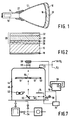
- the cathode ray tube shown in Figure 1 comprises an envelope formed by an optically transparent faceplate panel 10 which is connected to a conical portion 12, a neck 14 is connected to the conical portion 12.
- An electron gun 16 is disposed within the neck 14.
- a cathodoluminescent screen 18 is provided on the inside of the faceplate panel 10.
- An anti-reflection coating 20 is provided on the outside surface of the faceplate panel 10 which is composed of a mixed alkali glass substantially free of lead oxide (PbO).
- An electron beam (not shown) produced by the electron gun 16 is scanned over the screen by a deflection coil assembly 22 provided at the neck-conical portion transition of the envelope.
- the illustrated cathode ray tube may comprise a monochrome tube, a PTV tube or an oscilloscope tube.
- the invention can be applied to a shadow mask display tube or to any other display device because it is primarily directed to enhancing the contrast of an image by reducing reflections from the outer surface of the faceplate.
- the faceplate structure and anti-reflection coating 20 shown in Figure 2 have not been drawn to scale.
- the illustrated anti-reflection coating 20 comprises four contiguous layers 26, 28, 30, 32 applied by vacuum evaporation at ambient temperatures onto the faceplate panel 10.
- the layers 26 to 32 have different thickness and the layers 26 and 30 are of a material, such as Nb2O5, having a relatively high refractive index and the layers 28 and 32 are of a material, such as SiO2 having a relatively low refractive index.
- each of the layers 26 to 32 is selected having regard to the refractive index, n, of the material of each layer and the optical performance required, the thickness of each of the layers 26, 28 is of the order of ⁇ /8, that of the layer 30 is of the order of ⁇ /2 and that of the layer 32 is of the order of ⁇ /4, where ⁇ is equal to the desired centre wavelength selected from the eye sensitivity curve shown in Figure 3.
- One advantage of having layers of different thicknesses is that interference effects are reduced.
- Materials such as Nb2O5 and SiO2 form medium hardness layers when evaporated on to the unheated faceplate panel 10 at ambient temperature which is of the order of 80°C.
- unlike materials such as MgF2 these layers can be hardened subsequently by high temperature annealing to make them scratch resistant.
- the second layer 28 may comprise a different material from SiO2, such different materials including Al2O3, MgO, or CeO2. Some of the criteria for the selection of the material for this layer are that it has a refractive index between 1.4 and 1.8, and that it can be evaporated as a relatively hard layer which can be annealed to a harder layer subsequently.
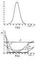
- Figure 3 is a sensitivity curve 34 of a human eye.
- the abscissa is wavelength, ⁇ , in nanometres (nm.) and the ordinate is calibrated in arbitrary units.
- the curve is generally Gaussian and has a peak value at about 550 nm.
- Figure 4 shows graphs of wavelength, ⁇ , against reflectance (R) in per cent of glass and the reflectances of coatings having 1, 2 or 3 filter layers.
- the reflectance of glass is shown by a horizontal line 36 having a reflectance value of 4.9%.
- an anti-reflection coating would ideally have a rectangular characteristic 38 shown in broken lines.
- a typical single layer anti-reflection coating has a characteristic shown by the chain-dot line 39 which has a minimum reflectance value at about 550 nm.
- a typical double layer V-coat filter characteristic is shown by the chain-double dot line 40 and has a minimum or zero reflectance over a short range of wavelengths which makes such an anti-reflection coating suitable for use on lasers.
- the characteristic of a 3-layer W coating is shown by the line 42.
- the presence of a third layer has the effect of pulling the flanks of the V-characteristic 40 sideways to produce a curve which is closer to the idealised characteristic. By providing 4 or more layers the reflectance curve obtained approximates closer to a rectangle.
- the layer thickness are of the order of ⁇ /8, ⁇ 8, ⁇ /2 and ⁇ /4 beginning from the glass substrate.
- Figure 5 is a graph of the reflectance (R) of a 4-layer anti-reflective coating made by the method made in accordance with the present invention.
- the anti-reflective coating comprises a first layer of Nb2O5, which has a high refractive index (2.14) and an optical thickness (n.d./ ⁇ ) 0.079, applied to the faceplate panel, a second layer of SiO2, which has a low refractive index (1.43) and an optical thickness 0.092, a third layer of Nb2O5 which has an optical thickness of 0.577 and an outermost layer of SiO2 which has an optical thickness of 0.249.
- Figure 6 is a graph of the reflective (R) of a 7-layer anti-reflective coating made by the method made in accordance with the present invention.
- the coating comprises alternate layers of SiO2 and Nb2O5 whose refractive indices (n) after annealing are 1.45 and 2.10, respectively.
- the innermost and outermost layers are of SiO2.
- the coating construction and optical thicknesses of the respective layers comprise:
- the illustrated curve is flatter compared to that shown in Figure 5 and that over the wavelength range specified, the reflectance is less than 1% and in this respect approaches the ideal curve 38 more closely.
- FIG. 7 illustrates diagrammatically an embodiment of the evaporation apparatus in which the filter layers of the anti-reflection coating are deposited on the faceplate panel 10.
- the apparatus comprises a Balzers BA510 optical coater 44 which includes a bell shaped cover 46 which is movable vertically relative to a base 48 for the introduction of, and removal of, faceplate panels 10 mounted in a rotatable support 50.
- the optical materials such as Nb2O5 and SiO2, are evaporated from an Airco - Temescal 8 kW four pocket electron gun 52.
- the electron gun 52 is arranged eccentrically in the space defined by the cover 46 in order to obtain a homogeneous thickness distribution on the rotating faceplate panels 10.
- a pumping system 54 consisting of a DIFF 1900 oil-diffusion pump and a DUO 35 rotary are coupled to the interior of the evaporation apparatus by way of an entry port in base 48.
- the effective pumping speed for N2 is 600 l/s and the ultimate pressure is 0,665 x 10 ⁇ 4 Pa (5 ⁇ 10 ⁇ 7) Torr.
- a liquid N2 Meissner trap is built-in for extra pumping speed for H2O during deposition.
- the deposition rates are controlled with a quartz-crystal thickness monitor 56 (for example a Leybold IC-6000).
- the optical layer thickness nd is measured during evaporation, using an optical monitor, for example a monitor made by Dynamic Optics, which comprises a light source 58 which shines its light through a window 60 in the bell cover. This light is reflected by an inclined mirror 62 through a monitoring glass 64 carried by the rotatable support 50.
- the light transmitted by the monitoring glass 64 is filtered by a monochromatic filter 66 before impinging on a detector 68 of the monitor.
- the monitor 56 follows the transmission and its interference effects at chosen wavelengths.
- An inlet 72 is provided in the cover 46 for the introduction of a mixture of argon (Ar) and oxygen (O2) under reduced pressure during substrate cleaning and of oxygen only during evaporation.
- An aluminium rod 74 is mounted inside the cover 46 and is connected to a power supply unit 76 in order to establish a glow discharge during the substrate cleaning phase.
- the faceplate panels which may have had their external surfaces mechanically roughened by a method as disclosed is European Patent Publication 0 131 341, are mounted in the rotatable support 50.
- the bell cover 46 is lowered onto the base 50.
- the system is evacuated to a pressure of the order of 0,665 x 10 ⁇ 3 Pa (5.10 ⁇ 6 Torr). Then the faceplate panels are cleaned using a glow discharge in an atmosphere of 90% Ar/10% O2 at a pressure of 13,3 to 1,33 Pa (10 ⁇ 1 to 10 ⁇ 2 Torr).
- the glow discharge current is of the order of 100 mA and the cleaning operation lasted for 15 minutes.
- the evaporation phases are carried out beginning with Nb2O5 under a partial oxygen pressure of 0,04 Pa (3.10 ⁇ 4Torr) at a rate of 0.7 nm/s (nanometres/sec).
- the electron gun 52 is switched to SiO2 which is deposited under a partial oxygen pressure of 0,04 Pa (3.10 ⁇ 4 Torr) at a rate of 1 nm./s.
- the evaporation apparatus is vented and the faceplate panels are removed.
- Annealing of the coating 20 takes place subsequently at a temperature of 450°C in air for about 1.5 hours. It is advantageous from the point of view of economising on the time required to make a cathode ray tube to anneal the coating during the normal processing of the cathode ray tube.
- Annealing not only hardens the layers but also changes their refractive indices. Accordingly when designing an anti-reflection coating, the performance specification must be related to the filter coating after annealing.
- the coating 20 may comprise at least 3 layers, four or more layers will provide a more practical anti-reflection coating because the material choice is greater.
Landscapes
- Physics & Mathematics (AREA)
- Chemical & Material Sciences (AREA)
- General Physics & Mathematics (AREA)
- Optics & Photonics (AREA)
- Engineering & Computer Science (AREA)
- General Chemical & Material Sciences (AREA)
- Life Sciences & Earth Sciences (AREA)
- Chemical Kinetics & Catalysis (AREA)
- Inorganic Chemistry (AREA)
- Geochemistry & Mineralogy (AREA)
- Materials Engineering (AREA)
- Organic Chemistry (AREA)
- Manufacturing & Machinery (AREA)
- Vessels, Lead-In Wires, Accessory Apparatuses For Cathode-Ray Tubes (AREA)
- Formation Of Various Coating Films On Cathode Ray Tubes And Lamps (AREA)
- Devices For Indicating Variable Information By Combining Individual Elements (AREA)
Claims (15)
- Verfahren zum Herstellen einer Wiedergabeanordnung, wobei dieses Verfahren die nachfolgenden Verfahrensschritte ausweist: das Anbringen einer gehärteten Antireflexionsbeschichtung auf einer äußeren Fläche einer Schirmträgerplaffe, wobei die Beschichtung durch Vakuumaufdampfen von wenigstens 3 Filterschichten auf die Schirmträgerplatte in einem Aufdampfungsgerät bei Raumtemperatur erfolgt, wobei das Material einer dieser Schichten einen hohen Brechungsindex gegenüber dem des Materials der Schirmträgerplatte hat und das Material einer anderen dieser Schichten einen niedrigen Brechungsindex gegenüber dem des Materials der Schirmträgerplatte hat, wobei die Materialien dieser Schichten nach dem Aufdampfen einen mittleren Hartegrad haben, und das Härten der genannten Schichten durch Glühen außerhalb des Aufdampfungsgeräts bei erhöhter Temperatur.
- Verfahren nach Anspruch 1, dadurch gekennzeichnet, daß das Material mit hohem Brechungsindex Nb₂O₅ enthält.
- Verfahren nach Anspruch 1 oder 2, dadurch gekennzeichnet, daß das Material mit niedrigem Brechungsindex SiO₂ enthält.
- Verfahren nach einem der Ansprüche 1 bis 3, dadurch gekennzeichnet, daß die Außenfläche des Schirmträgers mechanisch aufgerauht ist.
- Verfahren nach einem der Ansprüche 1 bis 4, dadurch gekennzeichnet, daß das Glühen der Schichten im normalen Bearbeitungsvorgang der Wiedergabeanordnung erfolgt.
- Verfahren nach einem der Ansprüche 1 bis 5, dadurch gekennzeichnet, daß der Schirmträger ein gemischtes Alkaliglas im wesentlichen frei von Bleioxid (PbO) enthält.
- Verfahren nach einem der Ansprüche 1 bis 6, dadurch gekennzeichnet, daß vier Filterschichten auf der Schirmträgerplatte niedergeschlagen werden, wobei diese Filterschichten abwechselnd aus (einem) Material mit hohem Brechungsindex und (einem) Material mit einem niedrigen Brechnungsindex bestehen, und daß eine erste auf der Schirmträgerplatte angebrachte Schicht einen hohen Brechungsindex hat.
- Verfahren nach Anspruch 7, dadurch gekennzeichnet, daß das Material der zweiten Schicht einen Brechungsindex zwischen 1,4 und 1,8 hat.
- Verfahren nach Anspruch 7 oder 8, dadurch gekennzeichnet, daß die Dicke jeder der Schichten sich zu den Brechungsindizes der aufgedampften Materialien verhält, und bei einer Vierschicht-Antireflexionsbeschichtung die ersten und zweiten Schichten je eine Dicke in der Größenordnung von λ/8, die dritte Schicht eine Dicke in der Größenordnung von λ/2 und die äußerste Schicht eine Dicke in der Größenordnung von λ/4 haben, worin λ gleich einer gewünschten gewählten zentralen Wellenlänge ist.
- Wiedergabeanordnung mit einem optisch transparenten Schirmträger, einer Antireflexionsbeschichtung auf einer äußeren Fläche des Schirmträgers, wobei die Antireflexionsbeschichtung wenigstens 3 aufgedampte Schichten enthält, die durch Glühen ausgehärtet wurden, wobei das Material einer dieser Schichten einen hohen Brechungsindex gegenüber dem des Materials des Schirmträgers und eine andere dieser Schichten einen niedrigen Brechungsindex gegenüber dem des Materials des Schirmträgers hat.
- Wiedergabeanordnung nach Anspruch 10, dadurch gekennzeichnet, daß das Material mit hohem Brechungsindex Nb₂O₅ ist.
- Wiedergabeanordnung nach Anspruch 10 oder 11, dadurch gekennzeichnet, daß das Material mit niedrigem Brechungsindex SiO₂ ist.
- Wiedergabeanordnung nach einem der Ansprüche 10, 11 oder 12, dadurch gekennzeichnet, daß die Außenfläche des Schirmträgers mechanisch aufgerauht ist.
- Wiedergabeanordnung nach einem der Ansprüche 10 bis 13, dadurch gekennzeichnet, daß die Beschichtung aus vier Schichten besteht, von denen die erste und zweite Schicht je eine Dicke in der Größenordnung von λ/8, die dritte Schicht eine Dicke in der Größenordnung von λ/2 und die äußerste Schicht eine Dicke in der Größenordnung von λ/4 haben, worin λ gleich einer gewünschten gewählten zentralen Wellenlänge ist.
- Wiedergabeanordnung nach einem oder mehreren der Ansprüche 10 bis 14, dadurch gekennzeichnet, daß der Schirmträger die Schirmträgerplatte einer Kathodenstrahlröhre und das Material des Schirmträgers ein gemischtes Alkaliglas im wesentlichen frei von Bleioxid (PbO) enthält.
Applications Claiming Priority (2)
| Application Number | Priority Date | Filing Date | Title |
|---|---|---|---|
| GB8621468 | 1986-09-05 | ||
| GB868621468A GB8621468D0 (en) | 1986-09-05 | 1986-09-05 | Display device |
Publications (3)
| Publication Number | Publication Date |
|---|---|
| EP0263541A2 EP0263541A2 (de) | 1988-04-13 |
| EP0263541A3 EP0263541A3 (en) | 1989-11-02 |
| EP0263541B1 true EP0263541B1 (de) | 1993-10-27 |
Family
ID=10603757
Family Applications (1)
| Application Number | Title | Priority Date | Filing Date |
|---|---|---|---|
| EP87201640A Expired - Lifetime EP0263541B1 (de) | 1986-09-05 | 1987-08-31 | Sichtvorrichtung und Verfahren zu ihrer Herstellung |
Country Status (7)
| Country | Link |
|---|---|
| US (1) | US4798994A (de) |
| EP (1) | EP0263541B1 (de) |
| JP (1) | JP2661919B2 (de) |
| KR (1) | KR950014063B1 (de) |
| CA (1) | CA1303119C (de) |
| DE (1) | DE3787949T2 (de) |
| GB (1) | GB8621468D0 (de) |
Families Citing this family (48)
| Publication number | Priority date | Publication date | Assignee | Title |
|---|---|---|---|---|
| US4931315A (en) * | 1986-12-17 | 1990-06-05 | Gte Products Corporation | Wide angle optical filters |
| NL8900070A (nl) * | 1989-01-12 | 1990-08-01 | Philips Nv | Inrichting voor het inspekteren van een interferentiefilter voor een projektie-televisiebeeldbuis. |
| US5138222A (en) * | 1989-06-27 | 1992-08-11 | Mitsubishi Denki Kabushiki Kaisha | Projection cathode ray tube having an interference filter |
| US5179318A (en) * | 1989-07-05 | 1993-01-12 | Nippon Sheet Glass Co., Ltd. | Cathode-ray tube with interference filter |
| JPH03138838A (ja) * | 1989-10-24 | 1991-06-13 | Mitsubishi Electric Corp | 投写型陰極線管 |
| DE4006804A1 (de) * | 1990-03-03 | 1991-09-05 | Renker Gmbh & Co Kg Zweigniede | Mehrschichtsystem mit hohem reflexionsvermoegen im infrarot-spektralbereich und mit hohem transmissionsvermoegen im sichtbaren bereich |
| JPH03261047A (ja) * | 1990-03-09 | 1991-11-20 | Toshiba Corp | 表示装置 |
| DE4014159A1 (de) * | 1990-05-03 | 1991-11-07 | Andreas Biedermann | Dekorierter gegenstand mit einer oberflaechenstruktur |
| FR2663486B1 (fr) * | 1990-06-15 | 1997-01-24 | Thomson Consumer Electronics | Dispositif de visualisation ou de projection d'images ou analogues. |
| DE69128192T2 (de) * | 1990-08-30 | 1998-05-28 | Viratec Thin Films Inc | Verfahren zur abscheidung von nioboxid enthaltenden optischen beschichtungen mittels reaktiver gleichstromzerstäubung |
| US5243255A (en) * | 1990-10-24 | 1993-09-07 | Mitsubishi Denki Kabushiki Kaisha | Cathode-ray tube with low reflectivity film |
| TW311694U (en) * | 1991-06-19 | 1997-07-21 | Toshiba Co Ltd Kk | Anti-reflection film |
| DE4130930A1 (de) * | 1991-09-13 | 1993-03-25 | Flachglas Ag | Vorsatzaggregat fuer bildschirme oder dergleichen |
| JP3355654B2 (ja) * | 1992-04-06 | 2002-12-09 | 松下電器産業株式会社 | 画像表示装置およびその製造方法 |
| DE69312017T2 (de) * | 1992-11-06 | 1997-12-04 | Toshiba Kawasaki Kk | Antireflektionsschicht und Anzeigegerät mit dieser Schicht |
| JP2981528B2 (ja) * | 1992-12-25 | 1999-11-22 | 三菱電機株式会社 | 陰極線管およびその製造方法 |
| US5521759A (en) * | 1993-06-07 | 1996-05-28 | National Research Council Of Canada | Optical filters for suppressing unwanted reflections |
| US5450238A (en) * | 1993-12-10 | 1995-09-12 | Viratec Thin Films, Inc. | Four-layer antireflection coating for deposition in in-like DC sputtering apparatus |
| JP3569538B2 (ja) * | 1993-12-27 | 2004-09-22 | 松下電器産業株式会社 | 画像表示装置 |
| DE69503598T2 (de) * | 1994-08-08 | 1999-03-04 | Philips Electronics Nv | Einen mit einer elektrisch leitfähigen schicht versehenen bildschirm enthaltende kathodenstrahlröhre |
| FR2730990B1 (fr) | 1995-02-23 | 1997-04-04 | Saint Gobain Vitrage | Substrat transparent a revetement anti-reflets |
| US5662395A (en) * | 1995-06-07 | 1997-09-02 | Nova Solutions, Inc. | Underdesk computer desk structure with antireflecting viewing window |
| WO1998035245A1 (en) * | 1997-02-11 | 1998-08-13 | Mcdonnell Douglas Corporation | High efficiency anti-reflectance coating and associated fabrication method |
| DE19708776C1 (de) * | 1997-03-04 | 1998-06-18 | Fraunhofer Ges Forschung | Entspiegelungsschicht sowie Verfahren zur Herstellung derselben |
| US5852513A (en) * | 1997-05-14 | 1998-12-22 | Optical Coating Laboratory, Inc. | Television filter |
| DE19752889C1 (de) * | 1997-11-28 | 1999-06-24 | Fraunhofer Ges Forschung | Verfahren zur Beschichtung von Oberflächen |
| KR100346422B1 (ko) * | 1998-08-26 | 2002-08-01 | 엘지전자주식회사 | 비반사 항정전기 필름 |
| US6529322B1 (en) * | 1999-01-27 | 2003-03-04 | University Of Georgia Research Foundation, Inc. | High contrast front and rear viewing surfaces for projection displays |
| FR2793889B1 (fr) * | 1999-05-20 | 2002-06-28 | Saint Gobain Vitrage | Substrat transparent a revetement anti-reflets |
| US6258218B1 (en) | 1999-10-22 | 2001-07-10 | Sola International Holdings, Ltd. | Method and apparatus for vacuum coating plastic parts |
| KR20010103321A (ko) * | 2000-05-09 | 2001-11-23 | 츄, 자우-지어 | 씨알티 표면의 고도전성 반사방지 코팅용 진공 스퍼터링및 습식 코팅의 조합 공정 |
| JP2002075227A (ja) * | 2000-06-14 | 2002-03-15 | Sharp Corp | 気体放電表示装置およびプラズマアドレス液晶表示装置ならびにその製造方法 |
| DE10034158C2 (de) * | 2000-07-10 | 2003-05-15 | Fraunhofer Ges Forschung | Reflexionsmindernde Beschichtung aus einem Wechselschichtsystem unterschiedlicher Schichtmaterialien mit jeweils niedrigerem und höherem Brechungsindex |
| US20030059195A1 (en) * | 2001-08-29 | 2003-03-27 | Brennan James F. | Optical devices using shaped optical fibers and methods for making optical devices with shaped optical fibers |
| US6589657B2 (en) | 2001-08-31 | 2003-07-08 | Von Ardenne Anlagentechnik Gmbh | Anti-reflection coatings and associated methods |
| US20030179455A1 (en) * | 2002-03-22 | 2003-09-25 | Jeffrey Hunt | Fingerprint resistant anti-reflection coatings for plastic substrates |
| US7293879B2 (en) | 2003-10-23 | 2007-11-13 | Hewlett-Packard Development Company, L.P. | Projection screen |
| US6987610B2 (en) * | 2003-10-23 | 2006-01-17 | Hewlett-Packard Development Company, L.P. | Projection screen |
| US7040764B2 (en) * | 2003-10-23 | 2006-05-09 | Hewlett-Packard Development Company, L.P. | Projection system using ambient light |
| US7846391B2 (en) * | 2006-05-22 | 2010-12-07 | Lumencor, Inc. | Bioanalytical instrumentation using a light source subsystem |
| US7709811B2 (en) * | 2007-07-03 | 2010-05-04 | Conner Arlie R | Light emitting diode illumination system |
| US8098375B2 (en) | 2007-08-06 | 2012-01-17 | Lumencor, Inc. | Light emitting diode illumination system |
| US8242462B2 (en) | 2009-01-23 | 2012-08-14 | Lumencor, Inc. | Lighting design of high quality biomedical devices |
| US8389957B2 (en) | 2011-01-14 | 2013-03-05 | Lumencor, Inc. | System and method for metered dosage illumination in a bioanalysis or other system |
| US8466436B2 (en) | 2011-01-14 | 2013-06-18 | Lumencor, Inc. | System and method for metered dosage illumination in a bioanalysis or other system |
| US8967811B2 (en) | 2012-01-20 | 2015-03-03 | Lumencor, Inc. | Solid state continuous white light source |
| US9217561B2 (en) | 2012-06-15 | 2015-12-22 | Lumencor, Inc. | Solid state light source for photocuring |
| US10544501B2 (en) * | 2013-12-31 | 2020-01-28 | Essilor International | Multi-layer assembly and method for controlling layer thicknesses |
Family Cites Families (16)
| Publication number | Priority date | Publication date | Assignee | Title |
|---|---|---|---|---|
| US2478385A (en) * | 1946-12-07 | 1949-08-09 | Libbey Owens Ford Glass Co | Multilayer low light reflecting film |
| US2612611A (en) * | 1950-06-23 | 1952-09-30 | Rauland Corp | Cathode-ray tube |
| CH291853A (de) * | 1950-09-27 | 1953-07-15 | Alois Dr Vogt | Interferenzfähige Schicht mit hohem Brechungsexponenten und Verfahren zur Herstellung dieser Schicht. |
| US2680205A (en) * | 1950-11-17 | 1954-06-01 | American Optical Corp | Cathode-ray tube and method of making same |
| US3185020A (en) * | 1961-09-07 | 1965-05-25 | Optical Coating Laboratory Inc | Three layer anti-reflection coating |
| US4065697A (en) * | 1969-02-17 | 1977-12-27 | Owens-Illinois, Inc. | Cathode-ray tube |
| US3635751A (en) * | 1969-04-03 | 1972-01-18 | Rca Corp | Lithium silicate glare-reducing coating and method of fabrication on a glass surface |
| JPS5133751B2 (de) * | 1972-07-27 | 1976-09-21 | ||
| FR2371497A1 (fr) * | 1976-06-23 | 1978-06-16 | Nippon Kogaku Kk | Revetement anti-reflechissant pour support de resine synthetique |
| US4277286A (en) * | 1980-02-19 | 1981-07-07 | Corning Glass Works | Lead-free glasses of high x-ray absorption for cathode ray tubes |
| JPS56138701A (en) * | 1980-03-31 | 1981-10-29 | Minolta Camera Co Ltd | Antireflection film |
| NL8301824A (nl) * | 1983-05-24 | 1984-12-17 | Philips Nv | Optisch element bestaande uit een doorzichtig substraat en een antireflectieve bekleding voor het golflengtegebied in het nabije infrarood. |
| NL8302460A (nl) * | 1983-07-11 | 1985-02-01 | Philips Nv | Werkwijze voor het verminderen van de reflectie van een doorzichtig beeldscherm en beeldscherm met verminderde reflectie. |
| JPS60252301A (ja) * | 1984-05-29 | 1985-12-13 | Asahi Glass Co Ltd | 耐熱性の向上された光学体 |
| DE3441948A1 (de) * | 1984-11-16 | 1986-05-28 | Bayer Ag, 5090 Leverkusen | Antireflex beschichtete, transparente abdeckung von zeichen, insbesondere fuer anzeigegeraete |
| JPS62105101A (ja) * | 1985-11-01 | 1987-05-15 | Asahi Chem Ind Co Ltd | 反射防止された光学部品 |
-
1986
- 1986-09-05 GB GB868621468A patent/GB8621468D0/en active Pending
-
1987
- 1987-08-31 EP EP87201640A patent/EP0263541B1/de not_active Expired - Lifetime
- 1987-08-31 DE DE87201640T patent/DE3787949T2/de not_active Expired - Fee Related
- 1987-09-01 CA CA000545808A patent/CA1303119C/en not_active Expired - Lifetime
- 1987-09-03 KR KR87009733A patent/KR950014063B1/ko not_active IP Right Cessation
- 1987-09-04 US US07/093,450 patent/US4798994A/en not_active Expired - Fee Related
- 1987-09-04 JP JP62220531A patent/JP2661919B2/ja not_active Expired - Lifetime
Also Published As
| Publication number | Publication date |
|---|---|
| EP0263541A3 (en) | 1989-11-02 |
| JPS6365478A (ja) | 1988-03-24 |
| US4798994A (en) | 1989-01-17 |
| KR950014063B1 (en) | 1995-11-20 |
| DE3787949T2 (de) | 1994-05-05 |
| EP0263541A2 (de) | 1988-04-13 |
| JP2661919B2 (ja) | 1997-10-08 |
| CA1303119C (en) | 1992-06-09 |
| KR880004524A (ko) | 1988-06-04 |
| DE3787949D1 (de) | 1993-12-02 |
| GB8621468D0 (en) | 1986-10-15 |
Similar Documents
| Publication | Publication Date | Title |
|---|---|---|
| EP0263541B1 (de) | Sichtvorrichtung und Verfahren zu ihrer Herstellung | |
| KR920003717B1 (ko) | 투명 시청 화면 및 상기 화면의 반사율 감소 방법 | |
| US5728456A (en) | Methods and apparatus for providing an absorbing, broad band, low brightness, antireflection coating | |
| US5068568A (en) | Cathode ray tube having multilayer interference filter | |
| US3604784A (en) | Antireflection coatings | |
| US5858519A (en) | Absorbing anti-reflection coatings for computer displays | |
| US4540914A (en) | Absorbing graded nitride film for high contrast display devices | |
| JPS6050233B2 (ja) | ルミネセンスの表示装置とその製法 | |
| GB2237141A (en) | Cathode ray tube face plate | |
| US4465337A (en) | Reduced reflectivity member and ion implantation method of fabrication | |
| EP0565026B1 (de) | Anzeigevorrichtung und Herstellungsverfahren | |
| US4157215A (en) | Photodeposition of CRT screen structures using cermet IC filter | |
| JPH09325211A (ja) | 光学フィルター | |
| JPH11171596A (ja) | 反射防止膜 | |
| JPS585855B2 (ja) | 半反射ガラス | |
| EP1873584A1 (de) | Vorderflächenspiegel | |
| Hutcheson et al. | A direct comparison of the visible and ultraviolet reflectance of aluminum films evaporated in conventional and ultra-high vacuum systems | |
| US4684846A (en) | Luminescent screen having restored cavities and display tube having such a screen | |
| US20050019528A1 (en) | Method of forming projecting film | |
| KR970000382B1 (ko) | 저반사 코팅유리 및 그 제조방법 | |
| EP0894331B1 (de) | Verfahren zur Herstellung einer Kathodenstrahlröhre | |
| RU2737824C1 (ru) | Дихроическое зеркало | |
| Pulker | Coatings on glass substrates | |
| KR970000902B1 (ko) | 저반사 코팅유리 및 그 제조방법 | |
| JPH10302683A (ja) | 発光表示デバイス |
Legal Events
| Date | Code | Title | Description |
|---|---|---|---|
| PUAI | Public reference made under article 153(3) epc to a published international application that has entered the european phase |
Free format text: ORIGINAL CODE: 0009012 |
|
| AK | Designated contracting states |
Kind code of ref document: A2 Designated state(s): DE ES FR GB IT NL |
|
| PUAL | Search report despatched |
Free format text: ORIGINAL CODE: 0009013 |
|
| AK | Designated contracting states |
Kind code of ref document: A3 Designated state(s): DE ES FR GB IT NL |
|
| 17P | Request for examination filed |
Effective date: 19900427 |
|
| 17Q | First examination report despatched |
Effective date: 19921111 |
|
| GRAA | (expected) grant |
Free format text: ORIGINAL CODE: 0009210 |
|
| AK | Designated contracting states |
Kind code of ref document: B1 Designated state(s): DE ES FR GB IT NL |
|
| PG25 | Lapsed in a contracting state [announced via postgrant information from national office to epo] |
Ref country code: NL Effective date: 19931027 |
|
| REF | Corresponds to: |
Ref document number: 3787949 Country of ref document: DE Date of ref document: 19931202 |
|
| ITF | It: translation for a ep patent filed |
Owner name: ING. C. GREGORJ S.P.A. |
|
| ET | Fr: translation filed | ||
| PG25 | Lapsed in a contracting state [announced via postgrant information from national office to epo] |
Ref country code: ES Free format text: LAPSE BECAUSE OF FAILURE TO SUBMIT A TRANSLATION OF THE DESCRIPTION OR TO PAY THE FEE WITHIN THE PRESCRIBED TIME-LIMIT Effective date: 19940207 |
|
| NLV1 | Nl: lapsed or annulled due to failure to fulfill the requirements of art. 29p and 29m of the patents act | ||
| PLBE | No opposition filed within time limit |
Free format text: ORIGINAL CODE: 0009261 |
|
| STAA | Information on the status of an ep patent application or granted ep patent |
Free format text: STATUS: NO OPPOSITION FILED WITHIN TIME LIMIT |
|
| 26N | No opposition filed | ||
| ITPR | It: changes in ownership of a european patent |
Owner name: CAMBIO RAGIONE SOCIALE;PHILIPS ELECTRONICS N.V. |
|
| REG | Reference to a national code |
Ref country code: FR Ref legal event code: CD |
|
| PGFP | Annual fee paid to national office [announced via postgrant information from national office to epo] |
Ref country code: DE Payment date: 19961025 Year of fee payment: 10 |
|
| PGFP | Annual fee paid to national office [announced via postgrant information from national office to epo] |
Ref country code: GB Payment date: 19970801 Year of fee payment: 11 |
|
| PGFP | Annual fee paid to national office [announced via postgrant information from national office to epo] |
Ref country code: FR Payment date: 19970819 Year of fee payment: 11 |
|
| PG25 | Lapsed in a contracting state [announced via postgrant information from national office to epo] |
Ref country code: DE Free format text: LAPSE BECAUSE OF NON-PAYMENT OF DUE FEES Effective date: 19980501 |
|
| PG25 | Lapsed in a contracting state [announced via postgrant information from national office to epo] |
Ref country code: GB Free format text: LAPSE BECAUSE OF NON-PAYMENT OF DUE FEES Effective date: 19980831 |
|
| REG | Reference to a national code |
Ref country code: FR Ref legal event code: CD |
|
| GBPC | Gb: european patent ceased through non-payment of renewal fee |
Effective date: 19980831 |
|
| PG25 | Lapsed in a contracting state [announced via postgrant information from national office to epo] |
Ref country code: FR Free format text: LAPSE BECAUSE OF NON-PAYMENT OF DUE FEES Effective date: 19990430 |
|
| REG | Reference to a national code |
Ref country code: FR Ref legal event code: ST |
|
| PG25 | Lapsed in a contracting state [announced via postgrant information from national office to epo] |
Ref country code: IT Free format text: LAPSE BECAUSE OF NON-PAYMENT OF DUE FEES;WARNING: LAPSES OF ITALIAN PATENTS WITH EFFECTIVE DATE BEFORE 2007 MAY HAVE OCCURRED AT ANY TIME BEFORE 2007. THE CORRECT EFFECTIVE DATE MAY BE DIFFERENT FROM THE ONE RECORDED. Effective date: 20050831 |