EP0260618A2 - Verfahren und Gerät zur Ermittlung von Produktensummen unter Verwendung von integrierten Schaltungen - Google Patents
Verfahren und Gerät zur Ermittlung von Produktensummen unter Verwendung von integrierten Schaltungen Download PDFInfo
- Publication number
- EP0260618A2 EP0260618A2 EP87113327A EP87113327A EP0260618A2 EP 0260618 A2 EP0260618 A2 EP 0260618A2 EP 87113327 A EP87113327 A EP 87113327A EP 87113327 A EP87113327 A EP 87113327A EP 0260618 A2 EP0260618 A2 EP 0260618A2
- Authority
- EP
- European Patent Office
- Prior art keywords
- products
- sum
- multiplier
- adder
- bits
- Prior art date
- Legal status (The legal status is an assumption and is not a legal conclusion. Google has not performed a legal analysis and makes no representation as to the accuracy of the status listed.)
- Granted
Links
Images


Classifications
-
- G—PHYSICS
- G06—COMPUTING OR CALCULATING; COUNTING
- G06F—ELECTRIC DIGITAL DATA PROCESSING
- G06F7/00—Methods or arrangements for processing data by operating upon the order or content of the data handled
- G06F7/38—Methods or arrangements for performing computations using exclusively denominational number representation, e.g. using binary, ternary, decimal representation
- G06F7/48—Methods or arrangements for performing computations using exclusively denominational number representation, e.g. using binary, ternary, decimal representation using non-contact-making devices, e.g. tube, solid state device; using unspecified devices
- G06F7/50—Adding; Subtracting
-
- G—PHYSICS
- G06—COMPUTING OR CALCULATING; COUNTING
- G06F—ELECTRIC DIGITAL DATA PROCESSING
- G06F7/00—Methods or arrangements for processing data by operating upon the order or content of the data handled
- G06F7/38—Methods or arrangements for performing computations using exclusively denominational number representation, e.g. using binary, ternary, decimal representation
- G06F7/48—Methods or arrangements for performing computations using exclusively denominational number representation, e.g. using binary, ternary, decimal representation using non-contact-making devices, e.g. tube, solid state device; using unspecified devices
- G06F7/52—Multiplying; Dividing
- G06F7/523—Multiplying only
- G06F7/53—Multiplying only in parallel-parallel fashion, i.e. both operands being entered in parallel
- G06F7/5324—Multiplying only in parallel-parallel fashion, i.e. both operands being entered in parallel partitioned, i.e. using repetitively a smaller parallel parallel multiplier or using an array of such smaller multipliers
-
- G—PHYSICS
- G06—COMPUTING OR CALCULATING; COUNTING
- G06F—ELECTRIC DIGITAL DATA PROCESSING
- G06F7/00—Methods or arrangements for processing data by operating upon the order or content of the data handled
- G06F7/38—Methods or arrangements for performing computations using exclusively denominational number representation, e.g. using binary, ternary, decimal representation
- G06F7/48—Methods or arrangements for performing computations using exclusively denominational number representation, e.g. using binary, ternary, decimal representation using non-contact-making devices, e.g. tube, solid state device; using unspecified devices
- G06F7/52—Multiplying; Dividing
- G06F7/523—Multiplying only
- G06F7/533—Reduction of the number of iteration steps or stages, e.g. using the Booth algorithm, log-sum, odd-even
- G06F7/5334—Reduction of the number of iteration steps or stages, e.g. using the Booth algorithm, log-sum, odd-even by using multiple bit scanning, i.e. by decoding groups of successive multiplier bits in order to select an appropriate precalculated multiple of the multiplicand as a partial product
- G06F7/5336—Reduction of the number of iteration steps or stages, e.g. using the Booth algorithm, log-sum, odd-even by using multiple bit scanning, i.e. by decoding groups of successive multiplier bits in order to select an appropriate precalculated multiple of the multiplicand as a partial product overlapped, i.e. with successive bitgroups sharing one or more bits being recoded into signed digit representation, e.g. using the Modified Booth Algorithm
- G06F7/5338—Reduction of the number of iteration steps or stages, e.g. using the Booth algorithm, log-sum, odd-even by using multiple bit scanning, i.e. by decoding groups of successive multiplier bits in order to select an appropriate precalculated multiple of the multiplicand as a partial product overlapped, i.e. with successive bitgroups sharing one or more bits being recoded into signed digit representation, e.g. using the Modified Booth Algorithm each bitgroup having two new bits, e.g. 2nd order MBA
-
- G—PHYSICS
- G06—COMPUTING OR CALCULATING; COUNTING
- G06F—ELECTRIC DIGITAL DATA PROCESSING
- G06F7/00—Methods or arrangements for processing data by operating upon the order or content of the data handled
- G06F7/38—Methods or arrangements for performing computations using exclusively denominational number representation, e.g. using binary, ternary, decimal representation
- G06F7/48—Methods or arrangements for performing computations using exclusively denominational number representation, e.g. using binary, ternary, decimal representation using non-contact-making devices, e.g. tube, solid state device; using unspecified devices
- G06F7/544—Methods or arrangements for performing computations using exclusively denominational number representation, e.g. using binary, ternary, decimal representation using non-contact-making devices, e.g. tube, solid state device; using unspecified devices for evaluating functions by calculation
- G06F7/5443—Sum of products
-
- G—PHYSICS
- G06—COMPUTING OR CALCULATING; COUNTING
- G06F—ELECTRIC DIGITAL DATA PROCESSING
- G06F2207/00—Indexing scheme relating to methods or arrangements for processing data by operating upon the order or content of the data handled
- G06F2207/38—Indexing scheme relating to groups G06F7/38 - G06F7/575
- G06F2207/3804—Details
- G06F2207/386—Special constructional features
- G06F2207/3884—Pipelining
Definitions
- the present invention relates to a method and a device for obtaining a sum of products using integrated circuits (IC's) and utilized in a picture (or image) processing system using a spatial filtering method, and in particular, to a method and a device for obtaining a sum of products using a predetermined number of multipliers and adders for summing the products.
- IC integrated circuits
- a device for obtaining a sum of products is used in a picture processing system or in radio communication equipment.
- each pixel of a picture is processed by the device, and as a result, a smoother, enhanced, or contour-emphatic picture is obtained.
- This device is applied in the processing of a picture from a weather satellite, a parts inspection apparatus in a factory, a viewing robot, or the like.
- the device is used as an element in a transversal equalizer, to increase the quality of the transmission signal.
- a sum of products is obtained by calculating the products of pairs of multiplicands and multipliers, and then add the total products.
- the number of devices used is in accordance with the scale of the operation. Namely, first a desired number of multipliers (number of pairs of the object to be multiplied) is provided. The products of these pairs are calculated by the multiplier and a plurality of products is obtained. The products are added two by two and a corresponding sum is obtained for each addition. Each sum is then further added two by two, and this calculation operation is repeated until the total sum of products is obtained.
- the only problem with the multipliers is the capacity of an IC to cope with the number of multipliers and the figure length of the operand applied to the multiplier.
- the "figure length", i.e., number of numeric characters, handled by this multiplier is determined by the figure length of the multiplicand and multiplier.
- the sums to be calculated increase as the processing advances. This requires a change of the scale of the adder in response to the stage at which the adder is located. That is, an IC having the same rating cannot be used for all of the adders.
- the present invention has been created to solve this problem, and satisfies the above operation needs by using a plurality of IC's having the same rating.
- An object of the present invention is to provide a method and a device for obtaining a sum of products by which the summing of products on an arbitrary scale can be carried out, without the limitation imposed by the capacity of an IC, by using a plurality of IC's each having a limited capacity and a certain rating.
- Another object of the present invention is to provide a method and a device for obtaining a sum of products wherein each multiplier can be calculated the product by dividing the multiplicand and/or multiplier by a predetermined figure length, and thus the required number of multipliers can be accommodated in one IC.
- a method for obtaining a sum of products wherein, when products between a pair of operands to be multiplied are calculated for a plurality of pairs and the sum for the plurality of products is calculated, the sum of products is obtained by using a predetermined multiplier means and adders to sum the products; comprising the following steps of: dividing a portion of, or entire, operands to be multiplied into a plurality of divisions having a predetermined figure length; obtaining a sum of products from each pair of operands having the same figure position as a group; adding, by another adder, the obtained sums of products group by group by shifting the figure position of the sums corresponding to the figure position of the operands in the group.
- a device for obtaining a sum of products comprising a plurality of integrated circuits each including a plurality of multiplier means, an adder group for adding products calculated by the multiplier means, and an adder having an external input, for adding the sum from the adder group to a calculation result from the preceding stage integrated circuit; wirings by which at least a portion of a multiplicand and a multiplier to be operated is divided by a predetermined number of figures, the divided figures are supplied to the multiplier means, and the products of the multiplicand and the multiplier having the same figure position are added; and by which the results of sum of products in each integrated circuit are supplied to the external input of the next stage integrated circuit with a figure shift in response to the figure position of the multiplicand and the multiplier without lower figures.
- the two numerical values are always 3 figures and 2 figures, and therefore, as long as the adder has the capacity to handle these figures, the adder will not overflow.
- the above-mentioned operating method is applied to the general operation for obtaining a sum of products.
- the multiplier comprises only one figure, if the multiplier comprises two figures, the multiplier can be divided in the same way as the multiplicand. In a practical device, binary numbers are used, and therefore, the operation is more complex than that of the above example. However, the calculation principle is the same.
- the integrated circuit 61 shown in Fig. 1 has been used.
- the IC 61 comprises four multipliers 62, three adders 63, and an adder 64.
- the adder 63 adds the results of the multiplied products, i.e., the products calculated by the multiplier 62, and the adder 64 adds the result of the adders 63 to a result from an external input.
- a pair of operands, i.e., a multiplicand and multiplier, are supplied to input terminals 65 and 66.
- the external input of the adder 64 is supplied to an external input terminal 67, and the operating result from another IC is also supplied to the terminal 67.
- the result of the sum of products is output from an output terminal 68.
- the IC 61 When the IC 61 performs a spatial filtering using a 3 ⁇ 3 matrix in a picture (or image) processing system, the sum of nine products must be obtained, and therefore, three IC's 61, 71, and 81 are connected as shown in Fig. 2.
- the multiplicand corresponding to the value of the picture element and the multiplier corresponds to the factor. Also in this example, if the pairs of multiplicand and multiplier are increased, then another IC must be added.
- the result obtained from another IC when the amount of data to be processed is increased, the result obtained from another IC must be supplied to the adder 64 through the terminal 67, and the result obtained in that IC added to the result obtained from another IC, by setting the lowest figures thereof at the same position and using the adder 64.
- the number of IC's is increased by one, the number of figures needed at the adder 64 becomes larger. Therefore, a problem arises in that the number of IC's must be limited to prevent an overflow of the obtained values at the adder 64. For example, assuming that the figure length of the multiplier 62 is 8 bits ⁇ 8 bits and the figure length of the adder 64 is 20 bits, then there must be an overflow because of the connection of four, or more than four, IC's 61.
- the figure length at the multiplier 62 is also limited, e.g., more than 8 bits, and thus an amount of data over this limit cannot be processed. Accordingly, because the scale of an IC is limited, one IC cannot include the necessary number of multipliers having a required figure length to operate the operand needed to obtain a sum of products corresponding to the amount of data.
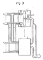
- Figure 3 shows an outline diagram of the wiring of a device according to a first embodiment of the present invention.
- An IC 1 comprises a plurality of multipliers 2-0 to 2-n, an adder group 3 adding the products obtained by the multipliers, and an adder 4 adding the addition result at the adder group 3 to a result obtained from another IC.
- X0 to X n are multiplicands.
- the number of multiplicands is nine.
- Each of the X0 to X n for example, comprises 8 bits. The 8 bits are divided into four lots of 2 bits, and each lot of 2 bits is connected to a different IC, and thus, four IC's must be used. Note, (n + 1) multipliers are necessary for each IC.
- the multipliers Y0 to Y n are, for example, 4 bits, respectively.
- the multiplier calculates the product using the extended Booth algorithm, and therefore, an input of 5 bits is supplied to each multiplier as shown in Fig. 6.
- the operand includes both the multiplicand and multiplier.
- X ⁇ x i ⁇ 2**i
- x i 0 or 1 and denotes the ith bit of X, and i is 0 at the lowest bit.
- 2**i indicates that i is an exponent of 2, i.e. 2**i indicates the ith power of 2.
- the product X ⁇ Y is shown as follows.
- the multiplicand X is divided by 2 bits, the products of each 2 bits and the multiplier Y are calculated, and each product is added by shifting two bits by two bits corresponding to the figure position before division.
- the above calculations are as follows.
- This equation shows that the following two operations (first and second operations) can obtain the same result.
- the multiplicands ⁇ X k ⁇ (non-division) are multiplied by the multipliers ⁇ Y k ⁇ and the products ⁇ X k ⁇ Y k ⁇ are added.
- the multiplicands ⁇ X k ⁇ are divided by two bits, the divided two bits being at the same figure position are collected, the products ⁇ (x k,i+1 ⁇ 2 + x k,i ) ⁇ Y k ⁇ of the collected bits and the multiplier ⁇ Y k ⁇ are obtained, the products are added with respect the same figure position, and the added products further added.
- the multiplier Y is divided by 3 bits, the multiplicands are multiplied by 0, ⁇ 1, or ⁇ 2 in response to the value (0 to 7) of the divided 3 bits, and the results are added together by shifting 2 bits by 2 bits.
- the multiplier is negative and indicated as a complement of 2
- the multiplicand X can be multiplied independently by 0, ⁇ 1, or ⁇ 2. That is, in this multiplier, the multiplier Y can be divided. The division of Y is explained later with reference to Figs. 4A and 4B.
- the products obtained at the multiplier 2-0 to 2-8 in the IC 1 are added together by the adder group 3, two by two.
- the result of sum of products obtained at each IC 1 is added to the result obtained from another IC allotted to another group by the adder 4, and then the addition result is output through the output terminal as a final sum of products.
- the result obtained from the other IC 1 is added by shifting certain figures in response to the figure position of the group belonging to the IC.
- the lower figures are shortened in the adding operation. Therefore, even an adder having limited figures will not overflow during the processing of the operand. That is, the limitation of the figure length does not limit the figure length of the operand at the adder.
- step 1 of the invention a plurality of pairs having operands to be multiplied are divided into a plurality of divided pairs by dividing the operand in each pair to a predetermined figure length corresponding to the capacity of an IC.
- step 2 the divided pairs having the same figure position are collected to form a group.
- the IC obtains a sum of products from the operand.
- step 3 the sum of products obtained in step 2 are added by another adder shifting the figure of the results corresponding to the figure position of each group.
- the adding operation by the adder can be shortened for the lower figures shifted by moving the figure position.
- the figure length at the adder is less than a predetermined length, and therefore, if a plurality of IC's are connected together, the adder will not overflow.
- the multiplier can calculate a multiplicand and multiplier having a small figure length, the number of multipliers and adders in one IC can be increased.
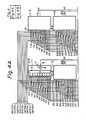
- the multiplier Y is divided by two.
- Data inputs D0 to D8 correspond to the multiplicands X0 to X n
- factors C0 to C8 correspond to the multiplier Y0 to Y n .
- the device in this embodiment comprises eight IC's which are denoted 1-1 to 1-8.
- Nine multipliers (2 bits ⁇ 4 bits) are provided in each IC.
- Each 8 bits data of D0 to D8 is divided into lots of 2 bits and the divided lots of 2 bits are connected to the IC's 1-1 to 1-4, respectively.
- the factors C0 to C8 (8 bits) are divided into two portions.
- the multipliers are denoted 2-0 to 2-8.
- the lower (1 : 0) (8 bits are denoted from the lower figure to the higher figure as 0 to 7 and, for example, the bits from 0 to 1 denoted as 1 : 0) of the 8 bits of D0 is supplied to one input of the multiplier 2-0 and (4 : 0) of C0 supplied to the other input of the multiplier 2-0.
- IC 1-1 (1 : 0) of D1 is supplied to one input of the multiplier 2-1 and (4 : 0) of C1 is supplied to the other input of the multiplier 2-1.
- IC 1-2 (3 : 2) of D0 is supplied to one input of the multiplier 2-0 and (4 : 0) of C0 is supplied to the other input of the multiplier 2-0.
- IC 1-5 (1 : 0) of D0 is supplied to one input of the multiplier 2-0, and (8 : 4) of C0 is supplied to the other input of the multiplier 2-0.
- the factors to be multiplied comprise 5 bits for using an extended Booth algorithm.
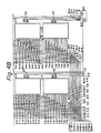
- a detail of the above-mentioned IC 1 is shown in Fig. 5.
- a multiplier group 2 comprises nine multipliers 2-0 to 2-8.
- An adder group 3 comprises eight adders.
- the adder 4 is provided with a terminal 7 for receiving an output from another IC and the output terminal thereof is referred to as numeral 8.
- each multiplier calculates the divided multiplicand and the divided multiplier and obtains a product.
- the adders add the nine products from the multipliers, and add the inputs while shifting the figure thereof in response to the figure positions of the multiplicand and multiplier.
- the multipliers 2-0 to 2-8 have, for example, a figure length of 2 ⁇ 4 bits.
- the adder 4 has, for example, the figure length of 12 bits.
- the reference numerals 5 and 6 denote input terminals for the divided multiplicand and the divided multiplier.
- Figure 6 shows a circuit diagram of an example of the multiplier.
- the multiplier calculates using the extended Booth algorithm.
- Reference numeral 21 denotes NAND circuit, 22 an AND circuit, 23 an OR circuit, 24 a NOR circuit, 25 an XOR (exclusive OR) circuit, 26 a NOT circuit, and 27 an adder of four bits.
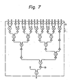
- Figure 7 shows a circuit diagram of an IC used in a second embodiment of the present invention.
- This IC 11 comprises flip-flop circuits 19 at preceding and succeeding stages of the multipliers and adders, different from the IC of the first embodiment.
- flip-flop circuits 19 By the provision of the flip-flop circuits 19, a pipeline operation in the operation of sum of products is possible.
- the processing flow of commands is divided into a maximum m steps and a maximum m commands are processed in parallel to realize a high speed processing.
- the input of the multiplier must be held from input application until the obtained result is output from the final adder, however, in the second embodiment, since whenever one operation is carried out the obtained result is held, the holding of the input is not necessary after the obtained result is stored in the flip-flop. Therefore, the operation efficiency is increased.
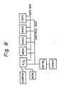
- a picture signal picked up through a camera is converted from analog to digital by an A/D converter, processed as a digital signal, and displayed on a monitor (MON.).
- the A/D converter is connected to a memory (MEM.), a convolution filter (CONV.), an operation apparatus (OPER.), and a first-in-first-out type memory (FIFO) through a data bus and control bus.
- the memory stores the picture signal, the picture signal is processed by a spatial filtering process through the convolution filter, and the apparatus obtains the picture signal.
- the FIFO stores the obtained results.
- the above elements or apparatus are controlled by a control board (CNTRL) through the control bus.
- the control board is connected to a control computer (COMP).
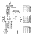
- a desired bus is selected by a bus selection device (BUS SEL.), the picture signal sent through the bus is supplied to an LSI, having a function of processing a sum of products obtained, directly or through a line memory (LINE M.) or line memories. Namely, the selected picture signal is directly supplied to an input "a”, supplied to an input "b” through one line memory, and supplied to an input "c” through two line memories.
- the digital picture signal value applied to the inputs "a", "b", and "c” is multiplied by factors ("F" input) stored in a ROM (read only memory) as shown in Fig. 10.
- a picture signal from CONV 1 (convolution filter 1) has been processed by a differential process, etc.
- the CONV 1 signal is added to the above-mentioned data (output "Z") processed by the LSI as an absolute addition.
- This processing is applied as a Sobel filter.
- the scaling device is a selector for obtaining the desired sum of products output.
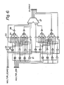
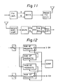
- FIG. 11 and Fig. 12 show a digital type transversal equalizer in a QAM (quadrature amplitude modulation) radio communication equipment to which the invention is applied.
- a transmission portion is shown in the upper portion of Fig. 11.
- a transmission interface TX INT
- the two digital signals are D/A converted and quadrature amplitude modulated by a modulator (MOD.) and the modulated signal is output through a radio transmission equipment (RADIO TX EQP.) and an antenna.
- RADIO TX EQP. radio transmission equipment
- the receiving side of the equipment is shown in the lower portion in Fig. 11.
- the signal received from an antenna is supplied to a demodulator (DEM) through a radio reception equipment (RADIO REC. EQP.).
- the signal is demodulated and supplied to an A/D converter (ADC).
- ADC A/D converter
- the output signal of the A/D converter is supplied to a transversal equalizer (TR. EQL), and the transversal equalizer outputs an I channel digital signal and a Q channel digital signal.
- TR. EQL transversal equalizer
- the details of the A/D converter and the transversal equalizer are shown in Fig. 12.
- the I and Q channel analog signals from the demodulator are supplied to four sum of products processing circuits through the A/D converters. After processing as shown in Fig. 12, the I channel digital signal and Q channel digital signal are obtained.
- the data signals at some moments from the A/D converter corresponds to multiplicands and the tap coefficients from a control portion (CONT) corresponds to the multipliers.
Landscapes
- Physics & Mathematics (AREA)
- Engineering & Computer Science (AREA)
- General Physics & Mathematics (AREA)
- Computational Mathematics (AREA)
- Mathematical Analysis (AREA)
- Pure & Applied Mathematics (AREA)
- Theoretical Computer Science (AREA)
- Mathematical Optimization (AREA)
- Computing Systems (AREA)
- General Engineering & Computer Science (AREA)
- Complex Calculations (AREA)
Applications Claiming Priority (2)
| Application Number | Priority Date | Filing Date | Title |
|---|---|---|---|
| JP218304/86 | 1986-09-17 | ||
| JP61218304A JPH0816903B2 (ja) | 1986-09-17 | 1986-09-17 | 積和演算回路 |
Publications (3)
| Publication Number | Publication Date |
|---|---|
| EP0260618A2 true EP0260618A2 (de) | 1988-03-23 |
| EP0260618A3 EP0260618A3 (en) | 1990-08-22 |
| EP0260618B1 EP0260618B1 (de) | 1994-11-30 |
Family
ID=16717739
Family Applications (1)
| Application Number | Title | Priority Date | Filing Date |
|---|---|---|---|
| EP87113327A Expired - Lifetime EP0260618B1 (de) | 1986-09-17 | 1987-09-11 | Verfahren und Gerät zur Ermittlung von Produktensummen unter Verwendung von integrierten Schaltungen |
Country Status (4)
| Country | Link |
|---|---|
| US (1) | US5138574A (de) |
| EP (1) | EP0260618B1 (de) |
| JP (1) | JPH0816903B2 (de) |
| KR (1) | KR910001053B1 (de) |
Cited By (2)
| Publication number | Priority date | Publication date | Assignee | Title |
|---|---|---|---|---|
| EP0418412A1 (de) * | 1989-09-20 | 1991-03-27 | Deutsche ITT Industries GmbH | Schaltungsanordnung zur Produktsummenberechnung |
| WO1997039404A1 (en) * | 1996-04-17 | 1997-10-23 | Advanced Micro Devices, Inc. | An execute unit configured to selectably interpret an operand as multiple operands or as a single operand |
Families Citing this family (4)
| Publication number | Priority date | Publication date | Assignee | Title |
|---|---|---|---|---|
| US5586070A (en) * | 1994-08-03 | 1996-12-17 | Chromatic Research, Inc. | Structure and method for embedding two small multipliers in a larger multiplier |
| EP1445949B1 (de) * | 1996-05-30 | 2006-06-28 | Sony Corporation | Schaltung und Verfahren zur Produktsummenberechnung |
| US6523055B1 (en) | 1999-01-20 | 2003-02-18 | Lsi Logic Corporation | Circuit and method for multiplying and accumulating the sum of two products in a single cycle |
| KR102434401B1 (ko) | 2019-06-14 | 2022-08-22 | 포항공과대학교 산학협력단 | 뉴럴 네트워크 가속기 |
Family Cites Families (8)
| Publication number | Priority date | Publication date | Assignee | Title |
|---|---|---|---|---|
| JPS5547420B2 (de) * | 1972-02-21 | 1980-11-29 | ||
| US3814924A (en) * | 1973-03-12 | 1974-06-04 | Control Data Corp | Pipeline binary multiplier |
| JPS57199044A (en) * | 1981-06-03 | 1982-12-06 | Fujitsu Ltd | Multiplying device |
| JPS59194242A (ja) * | 1983-04-19 | 1984-11-05 | Toshiba Corp | ディジタル乗算累積加算装置 |
| US4594680A (en) * | 1983-05-04 | 1986-06-10 | Sperry Corporation | Apparatus for performing quadratic convergence division in a large data processing system |
| JPH0640301B2 (ja) * | 1983-09-22 | 1994-05-25 | ソニー株式会社 | 並列乗算回路 |
| US4679164A (en) * | 1984-12-17 | 1987-07-07 | The United States Of America As Represented By The Secretary Of The Army | Digital high speed programmable convolver |
| JPS61220028A (ja) * | 1985-03-27 | 1986-09-30 | Hitachi Ltd | 乗算装置 |
-
1986
- 1986-09-17 JP JP61218304A patent/JPH0816903B2/ja not_active Expired - Lifetime
-
1987
- 1987-09-11 EP EP87113327A patent/EP0260618B1/de not_active Expired - Lifetime
- 1987-09-17 KR KR878710335A patent/KR910001053B1/ko not_active Expired
-
1991
- 1991-08-15 US US07/746,816 patent/US5138574A/en not_active Expired - Fee Related
Non-Patent Citations (5)
| Title |
|---|
| A MINI-MICRO CONFERENCE RECORD, May 1984, pages 1-10, Northeast, NY, US; N. LODHI et al.: "System solutions for a high-speed processor using innovative ICs" * |
| PROCEEDINGS IEEE INTERNATIONAL CONFERENCE ON COMPUTER DESIGN, 1984, pages 417-422, IEEE; D.A. HENLIN et al.: "A 25 MHz 16 BIT X 16 BIT pipelined multiplier" * |
| PROCEEDINGS OF THE 7TH SYMPOSIUM ON COMPUTER ARITHMETIC, Urbana, Illinois, 4th-6th June 1985, pages 38-43, IEEE, S.P. SMITH et al.: "Design of a fast inner product processor" * |
| RADIO FERNSEHEN ELEKTRONIK, vol. 33, no. 11, November 1984, pages 726-728, Ost-Berlin, DD; P. MEISTER: "Multiplikatormodul f}r K 1520" * |
| WESCON TECHNICAL PAPERS, 30th October/2nd November 1984, pages 1-4, Anaheim, California, LA, US; F. TOTH: "High performance CMOS DSP building block allows low power system optimization" * |
Cited By (4)
| Publication number | Priority date | Publication date | Assignee | Title |
|---|---|---|---|---|
| EP0418412A1 (de) * | 1989-09-20 | 1991-03-27 | Deutsche ITT Industries GmbH | Schaltungsanordnung zur Produktsummenberechnung |
| US5111422A (en) * | 1989-09-20 | 1992-05-05 | Deutsche Itt Industries Gmbh | Circuit arrangement for calculating product sums |
| WO1997039404A1 (en) * | 1996-04-17 | 1997-10-23 | Advanced Micro Devices, Inc. | An execute unit configured to selectably interpret an operand as multiple operands or as a single operand |
| US6092094A (en) * | 1996-04-17 | 2000-07-18 | Advanced Micro Devices, Inc. | Execute unit configured to selectably interpret an operand as multiple operands or as a single operand |
Also Published As
| Publication number | Publication date |
|---|---|
| KR880004375A (ko) | 1988-06-03 |
| KR910001053B1 (en) | 1991-02-23 |
| EP0260618A3 (en) | 1990-08-22 |
| JPH0816903B2 (ja) | 1996-02-21 |
| EP0260618B1 (de) | 1994-11-30 |
| JPS6373472A (ja) | 1988-04-04 |
| US5138574A (en) | 1992-08-11 |
Similar Documents
| Publication | Publication Date | Title |
|---|---|---|
| EP0045596A2 (de) | Bildverarbeitungsfilter | |
| US6131105A (en) | Calculation of a scalar product in a direct-type FIR filter | |
| JPS6132437Y2 (de) | ||
| JP2544326B2 (ja) | ディジタルフィルタ | |
| KR100302093B1 (ko) | 교차형디지탈유한임펄스응답필터에서이진입력신호를탭계수와승산시키는방법및회로배열과교차형디지탈필터의설계방법 | |
| EP0260618B1 (de) | Verfahren und Gerät zur Ermittlung von Produktensummen unter Verwendung von integrierten Schaltungen | |
| EP1094401B1 (de) | Datenberechnungvorrichtung | |
| US4328425A (en) | Filter for image pixels | |
| US5177703A (en) | Division circuit using higher radices | |
| AU569928B2 (en) | A method to compensate for the truncation error in a sampled signal and a device for carrying out the method | |
| US5798954A (en) | Digital filter device having a bit shifter unit | |
| JPH09325955A (ja) | 二乗和の平方根演算回路 | |
| US5424967A (en) | Shift and rounding circuit and method | |
| US5463572A (en) | Multi-nary and logic device | |
| US5912827A (en) | Digital filter with low rolloff factor | |
| US6272513B1 (en) | Multiplying device | |
| US5144572A (en) | Digital filter for filtering image data | |
| JPH08148991A (ja) | 多値論理和の演算装置 | |
| US5623434A (en) | Structure and method of using an arithmetic and logic unit for carry propagation stage of a multiplier | |
| CN109558109B (zh) | 数据运算装置及相关产品 | |
| EP0865682B1 (de) | Verwendung einkanaliger fir-filterarchitektur zur durchführung von kombinierter/paralleler filterung mehrerer (quadratur)-signale | |
| RU236695U1 (ru) | Устройство вычисления вероятности битовой ошибки для радиолинии с беспилотным летательным аппаратом при использовании квадратурной фазовой манипуляции | |
| US4748503A (en) | Data reduction circuit with a differential pulse code modulator for video signals | |
| KR100298127B1 (ko) | 덧셈기만을 사용한 비트 분리 구조의 고속 병렬 디지털 필터 | |
| CN1672327B (zh) | 数据处理电路 |
Legal Events
| Date | Code | Title | Description |
|---|---|---|---|
| PUAI | Public reference made under article 153(3) epc to a published international application that has entered the european phase |
Free format text: ORIGINAL CODE: 0009012 |
|
| AK | Designated contracting states |
Kind code of ref document: A2 Designated state(s): DE FR GB |
|
| PUAL | Search report despatched |
Free format text: ORIGINAL CODE: 0009013 |
|
| AK | Designated contracting states |
Kind code of ref document: A3 Designated state(s): DE FR GB |
|
| 17P | Request for examination filed |
Effective date: 19901010 |
|
| 17Q | First examination report despatched |
Effective date: 19920701 |
|
| RBV | Designated contracting states (corrected) |
Designated state(s): FR GB |
|
| REG | Reference to a national code |
Ref country code: DE Ref legal event code: 8566 |
|
| GRAA | (expected) grant |
Free format text: ORIGINAL CODE: 0009210 |
|
| AK | Designated contracting states |
Kind code of ref document: B1 Designated state(s): FR GB |
|
| ET | Fr: translation filed | ||
| PLBE | No opposition filed within time limit |
Free format text: ORIGINAL CODE: 0009261 |
|
| STAA | Information on the status of an ep patent application or granted ep patent |
Free format text: STATUS: NO OPPOSITION FILED WITHIN TIME LIMIT |
|
| 26N | No opposition filed | ||
| PGFP | Annual fee paid to national office [announced via postgrant information from national office to epo] |
Ref country code: FR Payment date: 19980909 Year of fee payment: 12 |
|
| PGFP | Annual fee paid to national office [announced via postgrant information from national office to epo] |
Ref country code: GB Payment date: 19981001 Year of fee payment: 12 |
|
| PG25 | Lapsed in a contracting state [announced via postgrant information from national office to epo] |
Ref country code: GB Free format text: LAPSE BECAUSE OF NON-PAYMENT OF DUE FEES Effective date: 19990911 |
|
| GBPC | Gb: european patent ceased through non-payment of renewal fee |
Effective date: 19990911 |
|
| PG25 | Lapsed in a contracting state [announced via postgrant information from national office to epo] |
Ref country code: FR Free format text: LAPSE BECAUSE OF NON-PAYMENT OF DUE FEES Effective date: 20000531 |
|
| REG | Reference to a national code |
Ref country code: FR Ref legal event code: ST |