EP0256053B1 - Matrix aus zusammengeschalteten dünnschichttransistoren und ihre herstellung - Google Patents
Matrix aus zusammengeschalteten dünnschichttransistoren und ihre herstellung Download PDFInfo
- Publication number
- EP0256053B1 EP0256053B1 EP19870900833 EP87900833A EP0256053B1 EP 0256053 B1 EP0256053 B1 EP 0256053B1 EP 19870900833 EP19870900833 EP 19870900833 EP 87900833 A EP87900833 A EP 87900833A EP 0256053 B1 EP0256053 B1 EP 0256053B1
- Authority
- EP
- European Patent Office
- Prior art keywords
- matrix
- film
- layer
- transistors
- source
- Prior art date
- Legal status (The legal status is an assumption and is not a legal conclusion. Google has not performed a legal analysis and makes no representation as to the accuracy of the status listed.)
- Expired - Lifetime
Links
- 239000011159 matrix material Substances 0.000 title claims abstract description 77
- 238000004519 manufacturing process Methods 0.000 title abstract description 22
- 239000004020 conductor Substances 0.000 claims abstract description 86
- XUIMIQQOPSSXEZ-UHFFFAOYSA-N Silicon Chemical compound [Si] XUIMIQQOPSSXEZ-UHFFFAOYSA-N 0.000 claims abstract description 42
- 229910052710 silicon Inorganic materials 0.000 claims abstract description 31
- 239000010703 silicon Substances 0.000 claims abstract description 31
- 239000000758 substrate Substances 0.000 claims abstract description 23
- 230000008021 deposition Effects 0.000 claims abstract description 21
- 239000000463 material Substances 0.000 claims abstract description 10
- 239000004065 semiconductor Substances 0.000 claims abstract description 10
- 230000005540 biological transmission Effects 0.000 claims abstract description 4
- 230000003287 optical effect Effects 0.000 claims abstract description 4
- 238000000034 method Methods 0.000 claims description 40
- 229920005989 resin Polymers 0.000 claims description 38
- 239000011347 resin Substances 0.000 claims description 38
- 238000005530 etching Methods 0.000 claims description 15
- 239000010409 thin film Substances 0.000 claims description 14
- 239000004973 liquid crystal related substance Substances 0.000 claims description 12
- 229910021417 amorphous silicon Inorganic materials 0.000 claims description 8
- 230000008030 elimination Effects 0.000 claims description 5
- 238000003379 elimination reaction Methods 0.000 claims description 5
- 239000012780 transparent material Substances 0.000 claims description 5
- 229910001887 tin oxide Inorganic materials 0.000 claims description 4
- 229910003437 indium oxide Inorganic materials 0.000 claims description 3
- PJXISJQVUVHSOJ-UHFFFAOYSA-N indium(iii) oxide Chemical compound [O-2].[O-2].[O-2].[In+3].[In+3] PJXISJQVUVHSOJ-UHFFFAOYSA-N 0.000 claims description 3
- 229920000642 polymer Polymers 0.000 claims description 3
- ATJFFYVFTNAWJD-UHFFFAOYSA-N Tin Chemical compound [Sn] ATJFFYVFTNAWJD-UHFFFAOYSA-N 0.000 claims description 2
- 239000007769 metal material Substances 0.000 claims description 2
- 239000010408 film Substances 0.000 claims 28
- 239000011248 coating agent Substances 0.000 claims 1
- 238000000576 coating method Methods 0.000 claims 1
- PEDCQBHIVMGVHV-UHFFFAOYSA-N Glycerine Chemical compound OCC(O)CO PEDCQBHIVMGVHV-UHFFFAOYSA-N 0.000 abstract 2
- 239000007788 liquid Substances 0.000 abstract 1
- 150000003376 silicon Chemical class 0.000 abstract 1
- 238000000151 deposition Methods 0.000 description 19
- 230000000873 masking effect Effects 0.000 description 15
- 239000012212 insulator Substances 0.000 description 8
- VYPSYNLAJGMNEJ-UHFFFAOYSA-N Silicium dioxide Chemical compound O=[Si]=O VYPSYNLAJGMNEJ-UHFFFAOYSA-N 0.000 description 6
- 238000001259 photo etching Methods 0.000 description 6
- 238000009413 insulation Methods 0.000 description 5
- 230000003071 parasitic effect Effects 0.000 description 4
- 238000003491 array Methods 0.000 description 3
- 239000003990 capacitor Substances 0.000 description 3
- 229910018487 Ni—Cr Inorganic materials 0.000 description 2
- BLRPTPMANUNPDV-UHFFFAOYSA-N Silane Chemical compound [SiH4] BLRPTPMANUNPDV-UHFFFAOYSA-N 0.000 description 2
- 238000005119 centrifugation Methods 0.000 description 2
- VNNRSPGTAMTISX-UHFFFAOYSA-N chromium nickel Chemical compound [Cr].[Ni] VNNRSPGTAMTISX-UHFFFAOYSA-N 0.000 description 2
- 230000005684 electric field Effects 0.000 description 2
- 239000000377 silicon dioxide Substances 0.000 description 2
- 229910052814 silicon oxide Inorganic materials 0.000 description 2
- 238000005507 spraying Methods 0.000 description 2
- XOLBLPGZBRYERU-UHFFFAOYSA-N tin dioxide Chemical compound O=[Sn]=O XOLBLPGZBRYERU-UHFFFAOYSA-N 0.000 description 2
- 238000007738 vacuum evaporation Methods 0.000 description 2
- 229910052782 aluminium Inorganic materials 0.000 description 1
- XAGFODPZIPBFFR-UHFFFAOYSA-N aluminium Chemical compound [Al] XAGFODPZIPBFFR-UHFFFAOYSA-N 0.000 description 1
- 239000006227 byproduct Substances 0.000 description 1
- 238000005229 chemical vapour deposition Methods 0.000 description 1
- 229910052681 coesite Inorganic materials 0.000 description 1
- 230000000295 complement effect Effects 0.000 description 1
- 229910052906 cristobalite Inorganic materials 0.000 description 1
- SLGWESQGEUXWJQ-UHFFFAOYSA-N formaldehyde;phenol Chemical compound O=C.OC1=CC=CC=C1 SLGWESQGEUXWJQ-UHFFFAOYSA-N 0.000 description 1
- 239000008246 gaseous mixture Substances 0.000 description 1
- 229910052738 indium Inorganic materials 0.000 description 1
- APFVFJFRJDLVQX-UHFFFAOYSA-N indium atom Chemical compound [In] APFVFJFRJDLVQX-UHFFFAOYSA-N 0.000 description 1
- 230000001678 irradiating effect Effects 0.000 description 1
- 229910052751 metal Inorganic materials 0.000 description 1
- 239000002184 metal Substances 0.000 description 1
- 230000005693 optoelectronics Effects 0.000 description 1
- 229920001568 phenolic resin Polymers 0.000 description 1
- 230000001681 protective effect Effects 0.000 description 1
- 230000005855 radiation Effects 0.000 description 1
- 235000012239 silicon dioxide Nutrition 0.000 description 1
- 229910052682 stishovite Inorganic materials 0.000 description 1
- 239000000126 substance Substances 0.000 description 1
- 230000001629 suppression Effects 0.000 description 1
- 229910052905 tridymite Inorganic materials 0.000 description 1
Images


Classifications
-
- H—ELECTRICITY
- H01—ELECTRIC ELEMENTS
- H01L—SEMICONDUCTOR DEVICES NOT COVERED BY CLASS H10
- H01L29/00—Semiconductor devices specially adapted for rectifying, amplifying, oscillating or switching and having potential barriers; Capacitors or resistors having potential barriers, e.g. a PN-junction depletion layer or carrier concentration layer; Details of semiconductor bodies or of electrodes thereof ; Multistep manufacturing processes therefor
- H01L29/66—Types of semiconductor device ; Multistep manufacturing processes therefor
- H01L29/68—Types of semiconductor device ; Multistep manufacturing processes therefor controllable by only the electric current supplied, or only the electric potential applied, to an electrode which does not carry the current to be rectified, amplified or switched
- H01L29/76—Unipolar devices, e.g. field effect transistors
- H01L29/772—Field effect transistors
- H01L29/78—Field effect transistors with field effect produced by an insulated gate
- H01L29/786—Thin film transistors, i.e. transistors with a channel being at least partly a thin film
- H01L29/78696—Thin film transistors, i.e. transistors with a channel being at least partly a thin film characterised by the structure of the channel, e.g. multichannel, transverse or longitudinal shape, length or width, doping structure, or the overlap or alignment between the channel and the gate, the source or the drain, or the contacting structure of the channel
-
- G—PHYSICS
- G02—OPTICS
- G02F—OPTICAL DEVICES OR ARRANGEMENTS FOR THE CONTROL OF LIGHT BY MODIFICATION OF THE OPTICAL PROPERTIES OF THE MEDIA OF THE ELEMENTS INVOLVED THEREIN; NON-LINEAR OPTICS; FREQUENCY-CHANGING OF LIGHT; OPTICAL LOGIC ELEMENTS; OPTICAL ANALOGUE/DIGITAL CONVERTERS
- G02F1/00—Devices or arrangements for the control of the intensity, colour, phase, polarisation or direction of light arriving from an independent light source, e.g. switching, gating or modulating; Non-linear optics
- G02F1/01—Devices or arrangements for the control of the intensity, colour, phase, polarisation or direction of light arriving from an independent light source, e.g. switching, gating or modulating; Non-linear optics for the control of the intensity, phase, polarisation or colour
- G02F1/13—Devices or arrangements for the control of the intensity, colour, phase, polarisation or direction of light arriving from an independent light source, e.g. switching, gating or modulating; Non-linear optics for the control of the intensity, phase, polarisation or colour based on liquid crystals, e.g. single liquid crystal display cells
- G02F1/133—Constructional arrangements; Operation of liquid crystal cells; Circuit arrangements
- G02F1/136—Liquid crystal cells structurally associated with a semi-conducting layer or substrate, e.g. cells forming part of an integrated circuit
- G02F1/1362—Active matrix addressed cells
- G02F1/1368—Active matrix addressed cells in which the switching element is a three-electrode device
-
- H—ELECTRICITY
- H01—ELECTRIC ELEMENTS
- H01L—SEMICONDUCTOR DEVICES NOT COVERED BY CLASS H10
- H01L29/00—Semiconductor devices specially adapted for rectifying, amplifying, oscillating or switching and having potential barriers; Capacitors or resistors having potential barriers, e.g. a PN-junction depletion layer or carrier concentration layer; Details of semiconductor bodies or of electrodes thereof ; Multistep manufacturing processes therefor
- H01L29/66—Types of semiconductor device ; Multistep manufacturing processes therefor
- H01L29/68—Types of semiconductor device ; Multistep manufacturing processes therefor controllable by only the electric current supplied, or only the electric potential applied, to an electrode which does not carry the current to be rectified, amplified or switched
- H01L29/76—Unipolar devices, e.g. field effect transistors
- H01L29/772—Field effect transistors
- H01L29/78—Field effect transistors with field effect produced by an insulated gate
- H01L29/786—Thin film transistors, i.e. transistors with a channel being at least partly a thin film
- H01L29/78651—Silicon transistors
- H01L29/7866—Non-monocrystalline silicon transistors
- H01L29/78663—Amorphous silicon transistors
- H01L29/78669—Amorphous silicon transistors with inverted-type structure, e.g. with bottom gate
Definitions
- the subject of the present invention is a matrix of interconnected thin-film transistors which can be used in particular for controlling the display of flat liquid crystal screens and its manufacturing process by photogravure techniques using at most three masking levels.
- TCM thin-film transistors
- This electronic memory which stores the video signal throughout the duration of the image is produced in the form of an active matrix of memory points or pixels each consisting of a TCM, the drain of which is connected to a point electrode forming a capacitor with a plate.
- Each pixel of the image is thus defined by the electrical state of the elementary capacitor thus formed which, depending on the electric field it generates, makes the corresponding point of the liquid crystal more or less transparent.
- the first technique described by FA HUNTLEY and published in "IBM Technical Disclosure Bulletin" 21, n ° 9, February 1979, comprises two masking levels: the first for photo-etching of the source-drain contacts and the second for the photo-etching of the conductive lines and the photogravure of the gate of the transistor.
- a photomask is placed on top of the stacked structure that was previously covered with a layer of resin. It is irradiated through this photomask to selectively polymerize the resin layer.
- a development phase removes the irradiated areas from this layer.
- the resin layer protected by the photomask remains after this development phase and serves as a mask for etching the layers of the stacked structure.
- this "grid over" technique does not offer the best characteristics for the manufacture of components used to produce active matrices for flat liquid crystal screens.
- the second technique called “grid below” requires in its implementation at least four masking levels.
- Such a technique has the drawback of requiring numerous levels of masking, which makes manufacture delicate, long and expensive. +) Proceedings of Japan Display, 1983, p. 356, "Amorphous Si TFT Active Matrix LCTV" and in EP-A-0 112 700.
- the subject of the present invention is precisely a matrix of thin-film transistors and its manufacturing method which makes it possible to largely overcome the drawbacks of the prior art by using the "grid below" technique and by engraving in a single masking operation. and in the same material all the source conductors of drains and point electrodes of the structure. They thus make it possible to reduce the number of masking levels from four to two (or three for a variant of the method). Thanks to the invention, better manufacturing yields are obtained, the production rates of the circuits are increased and the manufacturing costs reduced.
- the conductive and transparent material used for producing the drain source conductors and the pixel point electrodes can be tin oxide, indium oxide or mixed tin oxide / indium known in English terminology under the acronym ITO.
- the third light-opaque material used in the previous variant can be either a resin or a photosensitive polymer which is colored.
- the second layer of insulator which is deposited on the second conductive layer can, if necessary, be omitted.
- the two masking levels which in any case remain necessary in the implementation of the process which is the subject of the invention correspond for the first photogravure to the conductors of the transistor gates and for the second photogravure to the conductors of drains, of sources, and pixel point electrodes.
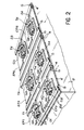
- the left part of the drawing represents a vertical section along AA ′ of the matrix structure of FIG. 1 and the right part of this same drawing represents a vertical section along BB 'of the same matrix structure of FIG. 1.
- Fig. 8 is a vertical section along CC 'of the matrix structure of FIG. 1.
- FIG. 1 In fig. 1 is shown, seen from above and in perspective view, a matrix of interconnected thin-film transistors, in the so-called cross-conductor embodiment.
- a substrate 2 On which rests an insulating layer 6 of silica SiO2 and where we see a number of transistors T1, T2, T3 and T4 located at the tops of the meshes of the network of the matrix.
- transistors T1, T2, T3 and T4 located at the tops of the meshes of the network of the matrix.
- the rows of the matrix are occupied by gate conductors such as G1, G2 and G3 arranged in the direction of the rows of the matrix and comprising a gate electrode proper 4 made of nickel-chromium embedded in the insulating layer 6 and surmounted by two semiconductor layers 8 and 10.
- source conductors S1 and S2 and drain conductors D1, D2 and D3 In the direction of the columns of the same matrix, which obviously make a right angle with the preceding lines, are arranged source conductors S1 and S2 and drain conductors D1, D2 and D3
- the grid lines G1, G2 extend continuously in the direction of the matrix lines, but the second layer 10 of semiconductors consists only of blocks located between each grid conductor and the source conductors and drains which cover them. In other words, this second semiconductor layer 10 is therefore discontinuous.
- this display is produced using a number of point electrodes EP1, EP2, EP3, EP4, which constitute the point electrode of each pixel of the screen and are each connected to an associated transistor, in this case the transistor T1 for the electrode EP1, the transistor T2 for the electrode EP2, the transistor T4 for the electrode EP4 etc ... It is, in a known manner, this point electrode of each pixel, which in connection with a conductive plate parallel to the matrix and between which is the liquid crystal, allows by application of a local electric field, to make this liquid crystal at each point more or less opaque or transparent.
- FIG. 2 shows a portion of an array of interconnected thin film transistors according to the invention in the so-called non-crossed conductor embodiment;
- the different lines of the matrix are constituted by conductors of gates G and of source S, joined at the level of each line.
- branches derived from grid conductors such as G1, G2, G3, G4, G5 and G6, and branches derived from source conductors S1, S2, S3, S4, S5 and S6.
- the point electrodes of the pixels of the display matrix are represented by the electrodes EP1, EP2, EP3, EP4, EP5 and EP6, connected by short conductors arranged in the direction of the lines of the matrix and connected to the drains of the various corresponding transistors T1, T2, T3, T4, T5 and T6.
- the different conductors of grids and sources have the same constitution as in the embodiment of FIG. 1, and in one case as in the other, the electrodes of each transistor are formed by the crossed overlap, in the two directions of the matrix, of the grid conductors by the source and drain conductors.
- the matrix structure of fig. 2, with non-crossed conductors, as shown in FIG. 2, offers an important advantage which is the suppression of the parasitic transistors.
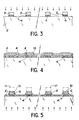
- the first step of the method consists in covering the substrate 2 with a first opaque metallic layer 4 preferably made of nickel-chromium.
- This first conductive layer 4 having for example a thickness of the order of 50 nm is obtained by deposition, for example by vacuum evaporation or by spraying.
- a layer of light-sensitive positive photosensitive resin having a wavelength of the order of 500 nm is deposited on the first conductive layer.
- This resin layer can in particular be deposited by centrifugation.
- resin it is possible to use phenolformaldehyde-based resins such as those sold by the company Hunt under the reference HPR 204.
- the resin layer is irradiated from above through a first mask (first masking level) (not shown in fig. 3) placed above the stacked structure and containing information on the shape of the grid conductors 4. ( The arrows in Fig. 1 indicate the direction of the irradiation).
- the first conductive layer 4 is then etched wet, the remaining resin 5 serving as a mask for said etching being eliminated once the etching operation is complete.
- This first photogravure applied to this first conductive layer makes it possible to constitute the gates 4 of the future transistors of the matrix.
- a first layer of insulator 6, preferably made of silicon oxide, is then deposited on the substrate 2 and the grids 4 of the transistors.
- This first layer of insulator having for example a thickness of 100 nm can be obtained at a deposition temperature of the order of 300 ° C. by the chemical vapor deposition technique, at low pressure or not, or by the glow discharge technique, in a radio frequency device, using a gaseous mixture of SiH4 and O2.
- a first layer of hydrogenated amorphous silicon 8 advantageously having a thickness varying from 50 nm to 150 nm.
- the thickness of the silicon layer is close to 100 nm and the deposition temperature on the order of 300 ° C.
- This first layer of silicon can be obtained by the glow discharge technique using the gas SiH4.
- This second silicon layer 10 deposited by the same technique and under the same deposition conditions as the first silicon layer, allows the subsequent production of ohmic contacts for the sources and drains of the TCMs of the matrix.
- the next step of the process consists in depositing, for example by centrifugation, on the second layer of hydrogenated amorphous silicon 10 of type n+, a layer of positive photosensitive resin, with the same characteristics as those of the resin previously used for etching the grids of the matrix transistors.
- the photosensitive resin layer is then irradiated from below through the substrate 2, the grid 4 serving as a mask for the irradiation (in FIG. 5, the arrows indicate the direction of the irradiation).
- the second layer 10 and the first layer 8 of silicon are then successively etched until the first insulating layer 6 is exposed, the remaining resin 11 serving as a mask for said etching (FIG. 5).
- the first and second layers of silicon (8 and 10) can be attacked chemically by partial and successive etchings, such as those described in French patent n ° 8516922 of November 15, 1985 and which allow '' on the flanks of the first and second layers of silicon a number of steps.
- a second conductive layer 12 is covered, for example having a thickness of 150 nm, and obtained by deposition, for example by vacuum evaporation or by spraying.
- deposition for example by vacuum evaporation or by spraying.
- the second conductive layer 12 is preferably made of tin and / or indium oxide ( ITO in terminology Anglo-Saxon). This transparent and conductive material will provide the substance for future source and drain conductors, as well as pixel point electrodes.
- the steps of the process according to the invention are completed by a second photoengraving applied using a second mask (second level), to the assembly second conductive layer 12 - second silicon layer 10 to delimit the source conductors and TCM drain of the matrix.
- second photoengraving applied using a second mask (second level), to the assembly second conductive layer 12 - second silicon layer 10 to delimit the source conductors and TCM drain of the matrix.
- This second photoengraving consists first of all of depositing on the second conductive layer 12 a layer of positive photosensitive resin 13 having the same characteristics as those of the resins previously used.
- the resin layer 13 is irradiated through a second masking level (not shown in FIG. 7) placed above the stacked structure, (The arrows on fig. 7 indicate the direction of the irradiation).
- the development of the resin layer makes it possible to keep from this layer only the areas 13a, 13b, 13c protected by the mask.
- the second conductive layer 12 and the second silicon layer 10 are then etched until the first silicon layer 8 is exposed.
- the remaining resin 13 serving as a mask for said etching is eliminated once the etching operation is complete.
- the position of the second mask is not critical; it can be placed in the horizontal direction with a certain latitude compatible nevertheless with the achievement of a correct positioning of the three electrodes one above the other. This faculty constitutes a simplification for the process which is the subject of the invention.
- each TCM is constituted by the part of the gate conductor which is located between the branch derived from the point electrode and the source conductor.
- the drain D and the source S of each TCM are respectively constituted by the crossed overlap of the gate conductor by the source and drain conductors.
- the first photoengraving of the method according to the invention applied to the metal layer 4 of the TCMs delimits the grids of the TCMs and the width of the grid conductor.
- the second photoengraving of the method according to the invention applied to the whole second conductive layer 12 - second silicon layer 10 delimits the sources S, the drains D of the TCMs and the point electrodes and determines the length of the channels of the TCMs which connect the drains at the sources of these.
- the grids 4 of the TCMs are formed by the part of the conductors G which is located between the branch derived from the point electrode and the branch derived from the source conductor.
- the drains D and the sources S are respectively formed by the crossed covering of the grid conductor by the source and drain conductors.
- the first and second photogravures of the method according to the invention respectively determine on the one hand the grids of the TCMs and the width of the grid conductors and on the other hand the sources S, the drains D of the TCMs and the length of the channels of the TCMs which connect the drains to the sources of these.
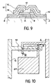
- Fig. 8 shows, in vertical section along CC 'of FIG. 1, the final state of a grid grid conductor.
- the drain D4 and the source S4 of the transistor T4 of fig. 1 we see, on the left, the drain D2 and the source S2 of the transistor T2. Note also in this figure the blocks of the second semiconductor layer 10 placed under the drain and source electrodes.
- a variant of the manufacturing method, according to the invention makes it possible to eliminate the parasitic transistor located on the other side of the source conductor, in the case of the structure with crossed conductors of FIG. 1, and to produce a screen opaque to light.
- this variant of the process consists in depositing a second layer of insulator 14 after the photoetching of the second conductive layer 12 and the dry silicon layer 10 and after the removal of the remaining resin 13 used for this photoengraving.
- the second insulating layer 14 is preferably made of silicon oxide and has for example a thickness of the order of 200 to 300 nm. It is obtained by the same technique as that used previously by the deposition of the first layer of insulation.
- a third layer 16 opaque to light is deposited over the entire structure, which may consist of the resin used for masking and which is colored black. If it is a photosensitive polymer that is being colored, it is possible to remove the second layer of insulation.
- the variant of the method according to the invention is completed by a third photoetching applied to the assembly, third opaque layer 16 - second layer of insulator 14 and first layer of silicon 8 to delimit a light screen 18 consisting of layers 16 and 14, which covers each transistor and which can be seen in plan and in dotted lines in FIG. 10.
- the shape of the screen 18 similar to that of the third mask of the third photogravure (third masking level) is shown in dotted lines.
- This screen 18 eliminates the parasitic transistor located on the other side of the gate line G, in the case of a matrix structure with crossed conductors.
- the parasitic transistor no longer has any influence on the capacitor constituted by the point electrode EP, the latter being screened by the source conductor S which is at low impedance.
- the method according to the invention thus makes it possible to produce in two masking planes or photogravures a matrix of transistors according to the structures of FIG. 2, the addition of a third masking plane or complementary photogravure also makes it possible to engrave on the - above each transistor of the matrix, an opaque protective cover, insulating it from light.
Landscapes
- Physics & Mathematics (AREA)
- Microelectronics & Electronic Packaging (AREA)
- Engineering & Computer Science (AREA)
- Power Engineering (AREA)
- General Physics & Mathematics (AREA)
- Ceramic Engineering (AREA)
- Nonlinear Science (AREA)
- Condensed Matter Physics & Semiconductors (AREA)
- Computer Hardware Design (AREA)
- Crystallography & Structural Chemistry (AREA)
- Optics & Photonics (AREA)
- Chemical & Material Sciences (AREA)
- Mathematical Physics (AREA)
- Thin Film Transistor (AREA)
- Liquid Crystal (AREA)
Claims (5)
- Matrix aus zusammengeschalteten Dünnfilmtransistoren insbesondere zur Steuerung der Anzeige auf flachen Flüssigkristallbildschirmen, bei denen der optische Transmissionszustand jedes Punkts des Schirms oder jedes Bildpunkts, der mit einem der Transistoren der Matrix verbunden ist, durch den elektrischen Zustand der Bildpunktelektrode (EP) des mit der Drainelektrode des entsprechenden Transistors verbundenen Bildpunkts gesteuert wird, welche auf einem Substrat die über Gateleiter (G), Sourceleiter (S) und Drainleiter (D), die entlang zweier senkrechter Richtungen der Matrix angeordnet sind, verbundenen Transistoren umfaßt, dadurch gekennzeichnet, daß:- die Gateleiter (G) eine Leiterbahn, die auf dem Substrat angeordnet und in einer isolierenden Schicht (6) vergraben ist, die die gesamte Oberfläche dieses Substrats bedeckt, und eine Leitung aus einem ersten halbleitenden Material, die diese Gate-Leiterbahn überlagert, umfassen;- die Sourceleiter (S) und die Drainleiter (D) ebenso wie die Bildpunktelektroden (EP) aus einem leitenden und transparenten Material gefertigt sind;- die Matrix von einem Typ mit nicht gekreuzten Leitern ist, in dem Sinne, daß die Zeilen der Matrix jedes Mal von einem Gateleiter und einem daneben angeordneten Sourceleiter belegt sind, wobei die Transistoren durch Überlagerung unter einem rechten Winkel von einen von dem Gateleiter abgeleitete Arm (G1, G2, G3, G4), der sich entlang den Spalten der Matrix befindet, mit einem von dem Sourceleiter abgeleiteten Arm (S1, S2, S3, S4), der sich entlang der Spalten der Matrix zwischen den Sourceleitern und Gateleitern, die zu zwei benachbarten Leitungen der Matrix gehören, befindet, und dem Drainleiter (D1, D2, D3, D4) parallel zur Richtung der Zeilen der Matrix gebildet wird.
- Verfahren zum Herstellen einer Matrix aus zusammengeschalteten Dünnfilmtransistoren insbesondere zur Steuerung der Anzeige auf flachen Flüssigkristallbildschirmen, bei denen der optische Transmissionszustand jedes Punkts des Schirms oder jedes Bildpunkts, der mit einem der Transistoren der Matrix verbunden ist, durch den elektrischen Zustand der Bildpunktelektrode (EP) des mit der Drainelektrode des entsprechenden Transistors verbundenen Bildpunkts gesteuert wird, welche auf einem Substrat die über Gateleiter (G), Sourceleiter (S) und Drainleiter (D), die entlang zweier senkrechter Richtungen der Matrix angeordnet sind, verbundenen Transistoren umfaßt, dadurch gekennzeichnet, daß es folgende Verfahrensschritte umfaßt:- Abscheiden einer ersten leitenden Schicht aus einem ersten metallischen, für das Licht undurchdringlichen Material (4) auf einem isolierenden Substrat,- erste Photoätzung mit Hilfe einer ersten Maske, die auf die erste Schicht angewandt wird, um entlang den Zeilen der Matrix die Leiterbahnen für Gates der zukünftigen Transistoren der Matrix zu bilden,- Abscheiden einer ersten isolierenden Schicht (6) auf dem Substrat (2) und der ersten leitenden Schicht,- Abscheiden einer ersten Schicht aus hydrogenisiertem, amorphen Silizium (8) auf der ersten isolierenden Schicht (6),- Abscheiden einer zweiten Schicht aus hydrogenisiertem, amorphen Silizium des Typs n⁺ (10) auf der ersten Siliziumschicht (8),- Abscheiden einer Schicht aus positivem Photolack (11) auf der zweiten Siliziumschicht (10),- Bestrahlen der Lackschicht von unten durch das Substrat, wobei der Gateleiter als Bestrahlungsmaske dient,- Entwickeln der Lackschicht, was zum Entfernen der bestrahlten Bereiche der Lackschicht führt,- Ätzen der ersten und zweiten Siliziumschichten (8) und (10) bis zum Freilegen der ersten Isolatorschicht (6), wobei der verbleibende Lack (11) als Maske für diese Ätzung dient,- Entfernen des verbliebenen Lacks (11),- Abscheiden einer zweiten Schicht aus einem zweiten transparenten, leitenden Material (12), das die künftigen Sourceleiter, Drainleiter und Bildpunktelektroden bildet, und anschließend einer neuen Lackschicht (13),- zweites Photoätzen mit Hilfe einer zweiten Maske, das von oben auf die Anordnung von Photolack (13), zweiter Leiterschicht (12) - zweiter Siliziumschicht angewandt wird, um die Sourceleiter, Drainleiter ebenso wie die Bildpunktelektroden der Matrix abzugrenzen.
- Verfahren nach Anspruch 2, dadurch gekennzeichnet, daß es nach den zweiten Photoätzen, das auf die Anordnung zweite Leiterschicht (12) - zweite Siliziumschicht (10) angewandt wird, und nach dem Entfernen des verbliebenen Lacks (13) folgende Schritte aufweist:- Abscheiden einer zweiten isolierenden Schicht (14) auf der zweiten leitenden Schicht (12),- Abscheiden einer Schicht aus einem dritten für das Licht undurchdringlichen Material (16) auf der zweiten Isolierschicht (14),- drittes Photoätzen mit Hilfe einer dritten Maske, das von oben auf die Anordnung von dritter, lichtundurchlässiger Schicht (16) - zweiter Isolatorschicht (14) und erster Siliziumschicht (8) angewandt wird, um einen Lichtschirm (18) abzugrenzen, der jeden Transistor schützt.
- Verfahren nach einen der Ansprüche 2 und 3, dadurch gekennzeichnet, daß das zweite leitende und transparente Material (12), das die Sourceleiter, Drainleiter und die Bildpunkte bildet, Zinn- und/oder Indiumoxyd ist.
- Verfahren nach einem der Ansprüche 2 bis 4, dadurch gekennzeichnet, daß das dritte, lichtundurchlässige Material (16) ein lichtempfindliches Polymer ist, welches man färbt.
Applications Claiming Priority (2)
| Application Number | Priority Date | Filing Date | Title |
|---|---|---|---|
| FR8600938A FR2593327B1 (fr) | 1986-01-23 | 1986-01-23 | Procede de fabrication d'un transistor en couches minces utilisant deux ou trois niveaux de masquage |
| FR8600938 | 1986-01-23 |
Publications (2)
| Publication Number | Publication Date |
|---|---|
| EP0256053A1 EP0256053A1 (de) | 1988-02-24 |
| EP0256053B1 true EP0256053B1 (de) | 1992-05-06 |
Family
ID=9331416
Family Applications (1)
| Application Number | Title | Priority Date | Filing Date |
|---|---|---|---|
| EP19870900833 Expired - Lifetime EP0256053B1 (de) | 1986-01-23 | 1987-01-22 | Matrix aus zusammengeschalteten dünnschichttransistoren und ihre herstellung |
Country Status (5)
| Country | Link |
|---|---|
| EP (1) | EP0256053B1 (de) |
| JP (1) | JPS63502220A (de) |
| DE (1) | DE3778783D1 (de) |
| FR (1) | FR2593327B1 (de) |
| WO (1) | WO1987004565A1 (de) |
Families Citing this family (5)
| Publication number | Priority date | Publication date | Assignee | Title |
|---|---|---|---|---|
| US4862234A (en) * | 1986-11-29 | 1989-08-29 | Sharp Kabushiki Kaisha | Thin-film transistor |
| FR2618011B1 (fr) * | 1987-07-10 | 1992-09-18 | Commissariat Energie Atomique | Procede de fabrication d'une cellule de memoire |
| JP3172841B2 (ja) * | 1992-02-19 | 2001-06-04 | 株式会社日立製作所 | 薄膜トランジスタとその製造方法及び液晶表示装置 |
| US5545576A (en) * | 1994-04-28 | 1996-08-13 | Casio Computer Co., Ltd. | Method for manufacturing a thin film transistor panel |
| US6882761B2 (en) * | 2001-01-22 | 2005-04-19 | The Furukawa Electric Co., Ltd. | Silicon platform for optical modules |
Family Cites Families (8)
| Publication number | Priority date | Publication date | Assignee | Title |
|---|---|---|---|---|
| US4024626A (en) * | 1974-12-09 | 1977-05-24 | Hughes Aircraft Company | Method of making integrated transistor matrix for flat panel liquid crystal display |
| FR2533072B1 (fr) * | 1982-09-14 | 1986-07-18 | Coissard Pierre | Procede de fabrication de circuits electroniques a base de transistors en couches minces et de condensateurs |
| JPS59119390A (ja) * | 1982-12-25 | 1984-07-10 | 株式会社東芝 | 薄膜トランジスタ回路 |
| JPS6066864A (ja) * | 1983-09-22 | 1985-04-17 | Seiko Instr & Electronics Ltd | Mis型薄膜トランジスタ |
| FR2553579B1 (fr) * | 1983-10-12 | 1985-12-27 | Commissariat Energie Atomique | Procede de fabrication d'un transistor en film mince a grille auto-alignee |
| JPS60105275A (ja) * | 1983-11-11 | 1985-06-10 | Seiko Instr & Electronics Ltd | Mis型薄膜トランジスタ |
| JPH065681B2 (ja) * | 1983-11-22 | 1994-01-19 | 松下電器産業株式会社 | 半導体装置の製造方法 |
| JPS60160173A (ja) * | 1984-01-30 | 1985-08-21 | Sharp Corp | 薄膜トランジスタ |
-
1986
- 1986-01-23 FR FR8600938A patent/FR2593327B1/fr not_active Expired
-
1987
- 1987-01-22 EP EP19870900833 patent/EP0256053B1/de not_active Expired - Lifetime
- 1987-01-22 JP JP50076387A patent/JPS63502220A/ja active Pending
- 1987-01-22 WO PCT/FR1987/000023 patent/WO1987004565A1/fr active IP Right Grant
- 1987-01-22 DE DE8787900833T patent/DE3778783D1/de not_active Expired - Lifetime
Also Published As
| Publication number | Publication date |
|---|---|
| FR2593327A1 (fr) | 1987-07-24 |
| JPS63502220A (ja) | 1988-08-25 |
| DE3778783D1 (de) | 1992-06-11 |
| FR2593327B1 (fr) | 1988-10-28 |
| WO1987004565A1 (fr) | 1987-07-30 |
| EP0256053A1 (de) | 1988-02-24 |
Similar Documents
| Publication | Publication Date | Title |
|---|---|---|
| EP0267824B1 (de) | Transistor-gesteuerter elektrooptischer Anzeigeschirm und Verfahren zu seiner Herstellung | |
| KR100846974B1 (ko) | Tft lcd 어레이 기판 및 그 제조 방법 | |
| FR2734082A1 (fr) | Procede de fabrication d'un condensateur de stockage dans un dispositif d'affichage a cristaux liquides et dispositif d'affichage a cristaux liquides | |
| EP0222668B1 (de) | Verfahren zum Herstellen eines Dünnschichttransistors mit in Bezug auf Source und Drain selbstausrichtendem Gate durch stufenweises Ätzen und danach hergestellter Transistor | |
| WO1984001239A1 (fr) | Procede de fabrication d'un ecran d'affichage a base de transistors en couches minces et de condensateurs | |
| FR2530057A1 (fr) | Afficheur a cristaux liquides en matrice de points | |
| FR2895805A1 (fr) | Substrat de reseau de transistors en couches minces pour un afficheur a cristaux liquides et son procede de fabrication | |
| EP0139585A1 (de) | Verfahren zum Herstellen eines Dünnfilmtransistors mit selbstausrichtendem Gate | |
| JPH11153809A (ja) | フォトマスク及びアクティブ素子アレイ基板の製造方法 | |
| US6465286B2 (en) | Method of fabricating an imager array | |
| EP0256053B1 (de) | Matrix aus zusammengeschalteten dünnschichttransistoren und ihre herstellung | |
| JPH0876144A (ja) | 薄膜トランジスタの製造方法 | |
| EP0415842B1 (de) | Verfahren zur Herstellung einer Anzeigetafel mit aktiver Matrix und invertierter Struktur | |
| JPS60100173A (ja) | 液晶表示装置の製造方法 | |
| JPH07159709A (ja) | エレクトロディスプレーシブアクチュエーチドミラーアレーおよびその製法 | |
| KR101172666B1 (ko) | 액정표시소자 및 그 제조방법 | |
| EP0368733B1 (de) | Herstellungsprozess für einen Anzeigebildschirm mit einer Transistormatrix, versehen mit einer lichtundurchlässigen Maske | |
| JP2666122B2 (ja) | 薄膜トランジスタ基板 | |
| JPH07142737A (ja) | 薄膜トランジスタの製造方法 | |
| KR100629686B1 (ko) | 액정표시장치용 어레이기판 제조방법 | |
| KR20000061175A (ko) | 액정표시장치의 제조방법 | |
| FR2901372A1 (fr) | Circuit integre d'affichage matriciel avec espaceur integre et procede de fabrication | |
| EP0228316A1 (de) | Verfahren zum Herstellen eines Dünnschichttransistors und so hergestellter Transistor | |
| FR2594580A1 (fr) | Procede de fabrication d'afficheur a cristaux liquides en matrice de points et afficheur ainsi fabrique | |
| FR2718885A1 (fr) | Procédé de fabrication d'un TFT étagé inverse. |
Legal Events
| Date | Code | Title | Description |
|---|---|---|---|
| PUAI | Public reference made under article 153(3) epc to a published international application that has entered the european phase |
Free format text: ORIGINAL CODE: 0009012 |
|
| 17P | Request for examination filed |
Effective date: 19870909 |
|
| AK | Designated contracting states |
Kind code of ref document: A1 Designated state(s): CH DE FR GB IT LI NL |
|
| 17Q | First examination report despatched |
Effective date: 19910211 |
|
| ITTA | It: last paid annual fee | ||
| GRAA | (expected) grant |
Free format text: ORIGINAL CODE: 0009210 |
|
| AK | Designated contracting states |
Kind code of ref document: B1 Designated state(s): CH DE FR GB IT LI NL |
|
| REF | Corresponds to: |
Ref document number: 3778783 Country of ref document: DE Date of ref document: 19920611 |
|
| ITF | It: translation for a ep patent filed |
Owner name: JACOBACCI & PERANI S.P.A. |
|
| GBT | Gb: translation of ep patent filed (gb section 77(6)(a)/1977) | ||
| PLBE | No opposition filed within time limit |
Free format text: ORIGINAL CODE: 0009261 |
|
| STAA | Information on the status of an ep patent application or granted ep patent |
Free format text: STATUS: NO OPPOSITION FILED WITHIN TIME LIMIT |
|
| 26N | No opposition filed | ||
| PGFP | Annual fee paid to national office [announced via postgrant information from national office to epo] |
Ref country code: CH Payment date: 19931231 Year of fee payment: 8 |
|
| PGFP | Annual fee paid to national office [announced via postgrant information from national office to epo] |
Ref country code: DE Payment date: 19940103 Year of fee payment: 8 |
|
| PGFP | Annual fee paid to national office [announced via postgrant information from national office to epo] |
Ref country code: GB Payment date: 19940113 Year of fee payment: 8 |
|
| PGFP | Annual fee paid to national office [announced via postgrant information from national office to epo] |
Ref country code: FR Payment date: 19940121 Year of fee payment: 8 |
|
| PGFP | Annual fee paid to national office [announced via postgrant information from national office to epo] |
Ref country code: NL Payment date: 19940131 Year of fee payment: 8 |
|
| PG25 | Lapsed in a contracting state [announced via postgrant information from national office to epo] |
Ref country code: GB Effective date: 19950122 |
|
| PG25 | Lapsed in a contracting state [announced via postgrant information from national office to epo] |
Ref country code: LI Effective date: 19950131 Ref country code: CH Effective date: 19950131 |
|
| PG25 | Lapsed in a contracting state [announced via postgrant information from national office to epo] |
Ref country code: NL Effective date: 19950801 |
|
| GBPC | Gb: european patent ceased through non-payment of renewal fee |
Effective date: 19950122 |
|
| PG25 | Lapsed in a contracting state [announced via postgrant information from national office to epo] |
Ref country code: FR Effective date: 19950929 |
|
| REG | Reference to a national code |
Ref country code: CH Ref legal event code: PL |
|
| NLV4 | Nl: lapsed or anulled due to non-payment of the annual fee |
Effective date: 19950801 |
|
| PG25 | Lapsed in a contracting state [announced via postgrant information from national office to epo] |
Ref country code: DE Effective date: 19951003 |
|
| REG | Reference to a national code |
Ref country code: FR Ref legal event code: ST |
|
| PG25 | Lapsed in a contracting state [announced via postgrant information from national office to epo] |
Ref country code: IT Free format text: LAPSE BECAUSE OF NON-PAYMENT OF DUE FEES;WARNING: LAPSES OF ITALIAN PATENTS WITH EFFECTIVE DATE BEFORE 2007 MAY HAVE OCCURRED AT ANY TIME BEFORE 2007. THE CORRECT EFFECTIVE DATE MAY BE DIFFERENT FROM THE ONE RECORDED. Effective date: 20050122 |