EP0256053B1 - Matrix of interconnected transistors in thin layers and production method thereof - Google Patents
Matrix of interconnected transistors in thin layers and production method thereof Download PDFInfo
- Publication number
- EP0256053B1 EP0256053B1 EP19870900833 EP87900833A EP0256053B1 EP 0256053 B1 EP0256053 B1 EP 0256053B1 EP 19870900833 EP19870900833 EP 19870900833 EP 87900833 A EP87900833 A EP 87900833A EP 0256053 B1 EP0256053 B1 EP 0256053B1
- Authority
- EP
- European Patent Office
- Prior art keywords
- matrix
- film
- layer
- transistors
- source
- Prior art date
- Legal status (The legal status is an assumption and is not a legal conclusion. Google has not performed a legal analysis and makes no representation as to the accuracy of the status listed.)
- Expired - Lifetime
Links
- 239000011159 matrix material Substances 0.000 title claims abstract description 77
- 238000004519 manufacturing process Methods 0.000 title abstract description 22
- 239000004020 conductor Substances 0.000 claims abstract description 86
- XUIMIQQOPSSXEZ-UHFFFAOYSA-N Silicon Chemical compound [Si] XUIMIQQOPSSXEZ-UHFFFAOYSA-N 0.000 claims abstract description 42
- 229910052710 silicon Inorganic materials 0.000 claims abstract description 31
- 239000010703 silicon Substances 0.000 claims abstract description 31
- 239000000758 substrate Substances 0.000 claims abstract description 23
- 230000008021 deposition Effects 0.000 claims abstract description 21
- 239000000463 material Substances 0.000 claims abstract description 10
- 239000004065 semiconductor Substances 0.000 claims abstract description 10
- 230000005540 biological transmission Effects 0.000 claims abstract description 4
- 230000003287 optical effect Effects 0.000 claims abstract description 4
- 238000000034 method Methods 0.000 claims description 40
- 229920005989 resin Polymers 0.000 claims description 38
- 239000011347 resin Substances 0.000 claims description 38
- 238000005530 etching Methods 0.000 claims description 15
- 239000010409 thin film Substances 0.000 claims description 14
- 239000004973 liquid crystal related substance Substances 0.000 claims description 12
- 229910021417 amorphous silicon Inorganic materials 0.000 claims description 8
- 230000008030 elimination Effects 0.000 claims description 5
- 238000003379 elimination reaction Methods 0.000 claims description 5
- 239000012780 transparent material Substances 0.000 claims description 5
- 229910001887 tin oxide Inorganic materials 0.000 claims description 4
- 229910003437 indium oxide Inorganic materials 0.000 claims description 3
- PJXISJQVUVHSOJ-UHFFFAOYSA-N indium(iii) oxide Chemical compound [O-2].[O-2].[O-2].[In+3].[In+3] PJXISJQVUVHSOJ-UHFFFAOYSA-N 0.000 claims description 3
- 229920000642 polymer Polymers 0.000 claims description 3
- ATJFFYVFTNAWJD-UHFFFAOYSA-N Tin Chemical compound [Sn] ATJFFYVFTNAWJD-UHFFFAOYSA-N 0.000 claims description 2
- 239000007769 metal material Substances 0.000 claims description 2
- 239000010408 film Substances 0.000 claims 28
- 239000011248 coating agent Substances 0.000 claims 1
- 238000000576 coating method Methods 0.000 claims 1
- PEDCQBHIVMGVHV-UHFFFAOYSA-N Glycerine Chemical compound OCC(O)CO PEDCQBHIVMGVHV-UHFFFAOYSA-N 0.000 abstract 2
- 239000007788 liquid Substances 0.000 abstract 1
- 150000003376 silicon Chemical class 0.000 abstract 1
- 238000000151 deposition Methods 0.000 description 19
- 230000000873 masking effect Effects 0.000 description 15
- 239000012212 insulator Substances 0.000 description 8
- VYPSYNLAJGMNEJ-UHFFFAOYSA-N Silicium dioxide Chemical compound O=[Si]=O VYPSYNLAJGMNEJ-UHFFFAOYSA-N 0.000 description 6
- 238000001259 photo etching Methods 0.000 description 6
- 238000009413 insulation Methods 0.000 description 5
- 230000003071 parasitic effect Effects 0.000 description 4
- 238000003491 array Methods 0.000 description 3
- 239000003990 capacitor Substances 0.000 description 3
- 229910018487 Ni—Cr Inorganic materials 0.000 description 2
- BLRPTPMANUNPDV-UHFFFAOYSA-N Silane Chemical compound [SiH4] BLRPTPMANUNPDV-UHFFFAOYSA-N 0.000 description 2
- 238000005119 centrifugation Methods 0.000 description 2
- VNNRSPGTAMTISX-UHFFFAOYSA-N chromium nickel Chemical compound [Cr].[Ni] VNNRSPGTAMTISX-UHFFFAOYSA-N 0.000 description 2
- 230000005684 electric field Effects 0.000 description 2
- 239000000377 silicon dioxide Substances 0.000 description 2
- 229910052814 silicon oxide Inorganic materials 0.000 description 2
- 238000005507 spraying Methods 0.000 description 2
- XOLBLPGZBRYERU-UHFFFAOYSA-N tin dioxide Chemical compound O=[Sn]=O XOLBLPGZBRYERU-UHFFFAOYSA-N 0.000 description 2
- 238000007738 vacuum evaporation Methods 0.000 description 2
- 229910052782 aluminium Inorganic materials 0.000 description 1
- XAGFODPZIPBFFR-UHFFFAOYSA-N aluminium Chemical compound [Al] XAGFODPZIPBFFR-UHFFFAOYSA-N 0.000 description 1
- 239000006227 byproduct Substances 0.000 description 1
- 238000005229 chemical vapour deposition Methods 0.000 description 1
- 229910052681 coesite Inorganic materials 0.000 description 1
- 230000000295 complement effect Effects 0.000 description 1
- 229910052906 cristobalite Inorganic materials 0.000 description 1
- SLGWESQGEUXWJQ-UHFFFAOYSA-N formaldehyde;phenol Chemical compound O=C.OC1=CC=CC=C1 SLGWESQGEUXWJQ-UHFFFAOYSA-N 0.000 description 1
- 239000008246 gaseous mixture Substances 0.000 description 1
- 229910052738 indium Inorganic materials 0.000 description 1
- APFVFJFRJDLVQX-UHFFFAOYSA-N indium atom Chemical compound [In] APFVFJFRJDLVQX-UHFFFAOYSA-N 0.000 description 1
- 230000001678 irradiating effect Effects 0.000 description 1
- 229910052751 metal Inorganic materials 0.000 description 1
- 239000002184 metal Substances 0.000 description 1
- 230000005693 optoelectronics Effects 0.000 description 1
- 229920001568 phenolic resin Polymers 0.000 description 1
- 230000001681 protective effect Effects 0.000 description 1
- 230000005855 radiation Effects 0.000 description 1
- 235000012239 silicon dioxide Nutrition 0.000 description 1
- 229910052682 stishovite Inorganic materials 0.000 description 1
- 239000000126 substance Substances 0.000 description 1
- 230000001629 suppression Effects 0.000 description 1
- 229910052905 tridymite Inorganic materials 0.000 description 1
Images


Classifications
-
- H—ELECTRICITY
- H01—ELECTRIC ELEMENTS
- H01L—SEMICONDUCTOR DEVICES NOT COVERED BY CLASS H10
- H01L29/00—Semiconductor devices specially adapted for rectifying, amplifying, oscillating or switching and having potential barriers; Capacitors or resistors having potential barriers, e.g. a PN-junction depletion layer or carrier concentration layer; Details of semiconductor bodies or of electrodes thereof ; Multistep manufacturing processes therefor
- H01L29/66—Types of semiconductor device ; Multistep manufacturing processes therefor
- H01L29/68—Types of semiconductor device ; Multistep manufacturing processes therefor controllable by only the electric current supplied, or only the electric potential applied, to an electrode which does not carry the current to be rectified, amplified or switched
- H01L29/76—Unipolar devices, e.g. field effect transistors
- H01L29/772—Field effect transistors
- H01L29/78—Field effect transistors with field effect produced by an insulated gate
- H01L29/786—Thin film transistors, i.e. transistors with a channel being at least partly a thin film
- H01L29/78696—Thin film transistors, i.e. transistors with a channel being at least partly a thin film characterised by the structure of the channel, e.g. multichannel, transverse or longitudinal shape, length or width, doping structure, or the overlap or alignment between the channel and the gate, the source or the drain, or the contacting structure of the channel
-
- G—PHYSICS
- G02—OPTICS
- G02F—OPTICAL DEVICES OR ARRANGEMENTS FOR THE CONTROL OF LIGHT BY MODIFICATION OF THE OPTICAL PROPERTIES OF THE MEDIA OF THE ELEMENTS INVOLVED THEREIN; NON-LINEAR OPTICS; FREQUENCY-CHANGING OF LIGHT; OPTICAL LOGIC ELEMENTS; OPTICAL ANALOGUE/DIGITAL CONVERTERS
- G02F1/00—Devices or arrangements for the control of the intensity, colour, phase, polarisation or direction of light arriving from an independent light source, e.g. switching, gating or modulating; Non-linear optics
- G02F1/01—Devices or arrangements for the control of the intensity, colour, phase, polarisation or direction of light arriving from an independent light source, e.g. switching, gating or modulating; Non-linear optics for the control of the intensity, phase, polarisation or colour
- G02F1/13—Devices or arrangements for the control of the intensity, colour, phase, polarisation or direction of light arriving from an independent light source, e.g. switching, gating or modulating; Non-linear optics for the control of the intensity, phase, polarisation or colour based on liquid crystals, e.g. single liquid crystal display cells
- G02F1/133—Constructional arrangements; Operation of liquid crystal cells; Circuit arrangements
- G02F1/136—Liquid crystal cells structurally associated with a semi-conducting layer or substrate, e.g. cells forming part of an integrated circuit
- G02F1/1362—Active matrix addressed cells
- G02F1/1368—Active matrix addressed cells in which the switching element is a three-electrode device
-
- H—ELECTRICITY
- H01—ELECTRIC ELEMENTS
- H01L—SEMICONDUCTOR DEVICES NOT COVERED BY CLASS H10
- H01L29/00—Semiconductor devices specially adapted for rectifying, amplifying, oscillating or switching and having potential barriers; Capacitors or resistors having potential barriers, e.g. a PN-junction depletion layer or carrier concentration layer; Details of semiconductor bodies or of electrodes thereof ; Multistep manufacturing processes therefor
- H01L29/66—Types of semiconductor device ; Multistep manufacturing processes therefor
- H01L29/68—Types of semiconductor device ; Multistep manufacturing processes therefor controllable by only the electric current supplied, or only the electric potential applied, to an electrode which does not carry the current to be rectified, amplified or switched
- H01L29/76—Unipolar devices, e.g. field effect transistors
- H01L29/772—Field effect transistors
- H01L29/78—Field effect transistors with field effect produced by an insulated gate
- H01L29/786—Thin film transistors, i.e. transistors with a channel being at least partly a thin film
- H01L29/78651—Silicon transistors
- H01L29/7866—Non-monocrystalline silicon transistors
- H01L29/78663—Amorphous silicon transistors
- H01L29/78669—Amorphous silicon transistors with inverted-type structure, e.g. with bottom gate
Definitions
- the subject of the present invention is a matrix of interconnected thin-film transistors which can be used in particular for controlling the display of flat liquid crystal screens and its manufacturing process by photogravure techniques using at most three masking levels.
- TCM thin-film transistors
- This electronic memory which stores the video signal throughout the duration of the image is produced in the form of an active matrix of memory points or pixels each consisting of a TCM, the drain of which is connected to a point electrode forming a capacitor with a plate.
- Each pixel of the image is thus defined by the electrical state of the elementary capacitor thus formed which, depending on the electric field it generates, makes the corresponding point of the liquid crystal more or less transparent.
- the first technique described by FA HUNTLEY and published in "IBM Technical Disclosure Bulletin" 21, n ° 9, February 1979, comprises two masking levels: the first for photo-etching of the source-drain contacts and the second for the photo-etching of the conductive lines and the photogravure of the gate of the transistor.
- a photomask is placed on top of the stacked structure that was previously covered with a layer of resin. It is irradiated through this photomask to selectively polymerize the resin layer.
- a development phase removes the irradiated areas from this layer.
- the resin layer protected by the photomask remains after this development phase and serves as a mask for etching the layers of the stacked structure.
- this "grid over" technique does not offer the best characteristics for the manufacture of components used to produce active matrices for flat liquid crystal screens.
- the second technique called “grid below” requires in its implementation at least four masking levels.
- Such a technique has the drawback of requiring numerous levels of masking, which makes manufacture delicate, long and expensive. +) Proceedings of Japan Display, 1983, p. 356, "Amorphous Si TFT Active Matrix LCTV" and in EP-A-0 112 700.
- the subject of the present invention is precisely a matrix of thin-film transistors and its manufacturing method which makes it possible to largely overcome the drawbacks of the prior art by using the "grid below" technique and by engraving in a single masking operation. and in the same material all the source conductors of drains and point electrodes of the structure. They thus make it possible to reduce the number of masking levels from four to two (or three for a variant of the method). Thanks to the invention, better manufacturing yields are obtained, the production rates of the circuits are increased and the manufacturing costs reduced.
- the conductive and transparent material used for producing the drain source conductors and the pixel point electrodes can be tin oxide, indium oxide or mixed tin oxide / indium known in English terminology under the acronym ITO.
- the third light-opaque material used in the previous variant can be either a resin or a photosensitive polymer which is colored.
- the second layer of insulator which is deposited on the second conductive layer can, if necessary, be omitted.
- the two masking levels which in any case remain necessary in the implementation of the process which is the subject of the invention correspond for the first photogravure to the conductors of the transistor gates and for the second photogravure to the conductors of drains, of sources, and pixel point electrodes.
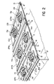
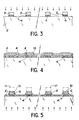
- the left part of the drawing represents a vertical section along AA ′ of the matrix structure of FIG. 1 and the right part of this same drawing represents a vertical section along BB 'of the same matrix structure of FIG. 1.
- Fig. 8 is a vertical section along CC 'of the matrix structure of FIG. 1.
- FIG. 1 In fig. 1 is shown, seen from above and in perspective view, a matrix of interconnected thin-film transistors, in the so-called cross-conductor embodiment.
- a substrate 2 On which rests an insulating layer 6 of silica SiO2 and where we see a number of transistors T1, T2, T3 and T4 located at the tops of the meshes of the network of the matrix.
- transistors T1, T2, T3 and T4 located at the tops of the meshes of the network of the matrix.
- the rows of the matrix are occupied by gate conductors such as G1, G2 and G3 arranged in the direction of the rows of the matrix and comprising a gate electrode proper 4 made of nickel-chromium embedded in the insulating layer 6 and surmounted by two semiconductor layers 8 and 10.
- source conductors S1 and S2 and drain conductors D1, D2 and D3 In the direction of the columns of the same matrix, which obviously make a right angle with the preceding lines, are arranged source conductors S1 and S2 and drain conductors D1, D2 and D3
- the grid lines G1, G2 extend continuously in the direction of the matrix lines, but the second layer 10 of semiconductors consists only of blocks located between each grid conductor and the source conductors and drains which cover them. In other words, this second semiconductor layer 10 is therefore discontinuous.
- this display is produced using a number of point electrodes EP1, EP2, EP3, EP4, which constitute the point electrode of each pixel of the screen and are each connected to an associated transistor, in this case the transistor T1 for the electrode EP1, the transistor T2 for the electrode EP2, the transistor T4 for the electrode EP4 etc ... It is, in a known manner, this point electrode of each pixel, which in connection with a conductive plate parallel to the matrix and between which is the liquid crystal, allows by application of a local electric field, to make this liquid crystal at each point more or less opaque or transparent.
- FIG. 2 shows a portion of an array of interconnected thin film transistors according to the invention in the so-called non-crossed conductor embodiment;
- the different lines of the matrix are constituted by conductors of gates G and of source S, joined at the level of each line.
- branches derived from grid conductors such as G1, G2, G3, G4, G5 and G6, and branches derived from source conductors S1, S2, S3, S4, S5 and S6.
- the point electrodes of the pixels of the display matrix are represented by the electrodes EP1, EP2, EP3, EP4, EP5 and EP6, connected by short conductors arranged in the direction of the lines of the matrix and connected to the drains of the various corresponding transistors T1, T2, T3, T4, T5 and T6.
- the different conductors of grids and sources have the same constitution as in the embodiment of FIG. 1, and in one case as in the other, the electrodes of each transistor are formed by the crossed overlap, in the two directions of the matrix, of the grid conductors by the source and drain conductors.
- the matrix structure of fig. 2, with non-crossed conductors, as shown in FIG. 2, offers an important advantage which is the suppression of the parasitic transistors.
- the first step of the method consists in covering the substrate 2 with a first opaque metallic layer 4 preferably made of nickel-chromium.
- This first conductive layer 4 having for example a thickness of the order of 50 nm is obtained by deposition, for example by vacuum evaporation or by spraying.
- a layer of light-sensitive positive photosensitive resin having a wavelength of the order of 500 nm is deposited on the first conductive layer.
- This resin layer can in particular be deposited by centrifugation.
- resin it is possible to use phenolformaldehyde-based resins such as those sold by the company Hunt under the reference HPR 204.
- the resin layer is irradiated from above through a first mask (first masking level) (not shown in fig. 3) placed above the stacked structure and containing information on the shape of the grid conductors 4. ( The arrows in Fig. 1 indicate the direction of the irradiation).
- the first conductive layer 4 is then etched wet, the remaining resin 5 serving as a mask for said etching being eliminated once the etching operation is complete.
- This first photogravure applied to this first conductive layer makes it possible to constitute the gates 4 of the future transistors of the matrix.
- a first layer of insulator 6, preferably made of silicon oxide, is then deposited on the substrate 2 and the grids 4 of the transistors.
- This first layer of insulator having for example a thickness of 100 nm can be obtained at a deposition temperature of the order of 300 ° C. by the chemical vapor deposition technique, at low pressure or not, or by the glow discharge technique, in a radio frequency device, using a gaseous mixture of SiH4 and O2.
- a first layer of hydrogenated amorphous silicon 8 advantageously having a thickness varying from 50 nm to 150 nm.
- the thickness of the silicon layer is close to 100 nm and the deposition temperature on the order of 300 ° C.
- This first layer of silicon can be obtained by the glow discharge technique using the gas SiH4.
- This second silicon layer 10 deposited by the same technique and under the same deposition conditions as the first silicon layer, allows the subsequent production of ohmic contacts for the sources and drains of the TCMs of the matrix.
- the next step of the process consists in depositing, for example by centrifugation, on the second layer of hydrogenated amorphous silicon 10 of type n+, a layer of positive photosensitive resin, with the same characteristics as those of the resin previously used for etching the grids of the matrix transistors.
- the photosensitive resin layer is then irradiated from below through the substrate 2, the grid 4 serving as a mask for the irradiation (in FIG. 5, the arrows indicate the direction of the irradiation).
- the second layer 10 and the first layer 8 of silicon are then successively etched until the first insulating layer 6 is exposed, the remaining resin 11 serving as a mask for said etching (FIG. 5).
- the first and second layers of silicon (8 and 10) can be attacked chemically by partial and successive etchings, such as those described in French patent n ° 8516922 of November 15, 1985 and which allow '' on the flanks of the first and second layers of silicon a number of steps.
- a second conductive layer 12 is covered, for example having a thickness of 150 nm, and obtained by deposition, for example by vacuum evaporation or by spraying.
- deposition for example by vacuum evaporation or by spraying.
- the second conductive layer 12 is preferably made of tin and / or indium oxide ( ITO in terminology Anglo-Saxon). This transparent and conductive material will provide the substance for future source and drain conductors, as well as pixel point electrodes.
- the steps of the process according to the invention are completed by a second photoengraving applied using a second mask (second level), to the assembly second conductive layer 12 - second silicon layer 10 to delimit the source conductors and TCM drain of the matrix.
- second photoengraving applied using a second mask (second level), to the assembly second conductive layer 12 - second silicon layer 10 to delimit the source conductors and TCM drain of the matrix.
- This second photoengraving consists first of all of depositing on the second conductive layer 12 a layer of positive photosensitive resin 13 having the same characteristics as those of the resins previously used.
- the resin layer 13 is irradiated through a second masking level (not shown in FIG. 7) placed above the stacked structure, (The arrows on fig. 7 indicate the direction of the irradiation).
- the development of the resin layer makes it possible to keep from this layer only the areas 13a, 13b, 13c protected by the mask.
- the second conductive layer 12 and the second silicon layer 10 are then etched until the first silicon layer 8 is exposed.
- the remaining resin 13 serving as a mask for said etching is eliminated once the etching operation is complete.
- the position of the second mask is not critical; it can be placed in the horizontal direction with a certain latitude compatible nevertheless with the achievement of a correct positioning of the three electrodes one above the other. This faculty constitutes a simplification for the process which is the subject of the invention.
- each TCM is constituted by the part of the gate conductor which is located between the branch derived from the point electrode and the source conductor.
- the drain D and the source S of each TCM are respectively constituted by the crossed overlap of the gate conductor by the source and drain conductors.
- the first photoengraving of the method according to the invention applied to the metal layer 4 of the TCMs delimits the grids of the TCMs and the width of the grid conductor.
- the second photoengraving of the method according to the invention applied to the whole second conductive layer 12 - second silicon layer 10 delimits the sources S, the drains D of the TCMs and the point electrodes and determines the length of the channels of the TCMs which connect the drains at the sources of these.
- the grids 4 of the TCMs are formed by the part of the conductors G which is located between the branch derived from the point electrode and the branch derived from the source conductor.
- the drains D and the sources S are respectively formed by the crossed covering of the grid conductor by the source and drain conductors.
- the first and second photogravures of the method according to the invention respectively determine on the one hand the grids of the TCMs and the width of the grid conductors and on the other hand the sources S, the drains D of the TCMs and the length of the channels of the TCMs which connect the drains to the sources of these.
- Fig. 8 shows, in vertical section along CC 'of FIG. 1, the final state of a grid grid conductor.
- the drain D4 and the source S4 of the transistor T4 of fig. 1 we see, on the left, the drain D2 and the source S2 of the transistor T2. Note also in this figure the blocks of the second semiconductor layer 10 placed under the drain and source electrodes.
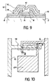
- a variant of the manufacturing method, according to the invention makes it possible to eliminate the parasitic transistor located on the other side of the source conductor, in the case of the structure with crossed conductors of FIG. 1, and to produce a screen opaque to light.
- this variant of the process consists in depositing a second layer of insulator 14 after the photoetching of the second conductive layer 12 and the dry silicon layer 10 and after the removal of the remaining resin 13 used for this photoengraving.
- the second insulating layer 14 is preferably made of silicon oxide and has for example a thickness of the order of 200 to 300 nm. It is obtained by the same technique as that used previously by the deposition of the first layer of insulation.
- a third layer 16 opaque to light is deposited over the entire structure, which may consist of the resin used for masking and which is colored black. If it is a photosensitive polymer that is being colored, it is possible to remove the second layer of insulation.
- the variant of the method according to the invention is completed by a third photoetching applied to the assembly, third opaque layer 16 - second layer of insulator 14 and first layer of silicon 8 to delimit a light screen 18 consisting of layers 16 and 14, which covers each transistor and which can be seen in plan and in dotted lines in FIG. 10.
- the shape of the screen 18 similar to that of the third mask of the third photogravure (third masking level) is shown in dotted lines.
- This screen 18 eliminates the parasitic transistor located on the other side of the gate line G, in the case of a matrix structure with crossed conductors.
- the parasitic transistor no longer has any influence on the capacitor constituted by the point electrode EP, the latter being screened by the source conductor S which is at low impedance.
- the method according to the invention thus makes it possible to produce in two masking planes or photogravures a matrix of transistors according to the structures of FIG. 2, the addition of a third masking plane or complementary photogravure also makes it possible to engrave on the - above each transistor of the matrix, an opaque protective cover, insulating it from light.
Landscapes
- Physics & Mathematics (AREA)
- Microelectronics & Electronic Packaging (AREA)
- Engineering & Computer Science (AREA)
- Power Engineering (AREA)
- General Physics & Mathematics (AREA)
- Ceramic Engineering (AREA)
- Nonlinear Science (AREA)
- Condensed Matter Physics & Semiconductors (AREA)
- Computer Hardware Design (AREA)
- Crystallography & Structural Chemistry (AREA)
- Optics & Photonics (AREA)
- Chemical & Material Sciences (AREA)
- Mathematical Physics (AREA)
- Thin Film Transistor (AREA)
- Liquid Crystal (AREA)
Abstract
Description
La présente invention a pour objet une matrice de transistors en couches minces interconnectés utilisables notamment pour la commande de l'affichage d'écrans plats à cristaux liquides et son procédé de fabrication par les techniques de photogravure utilisant au maximum trois niveaux de masquage.The subject of the present invention is a matrix of interconnected thin-film transistors which can be used in particular for controlling the display of flat liquid crystal screens and its manufacturing process by photogravure techniques using at most three masking levels.
D'une façon générale, elle permet la fabrication des composants semi-conducteurs en couches minces pouvant servir au multiplexage de tels composants disposés sous forme matricielle, ainsi qu'à la réalisation de dispositifs à transfert de charge (DTC en abrégé).In general, it allows the production of semiconductor components in thin layers which can be used for multiplexing such components arranged in matrix form, as well as for the production of charge transfer devices (DTC for short).
Plus particulièrement, elle permet la fabrication de matrices de transistors en couches minces (TCM en abrégé) pouvant servir en opto-électronique à la réalisation de la mémoire électronique des écrans plats à cristaux liquides. Cette mémoire électronique qui stocke le signal vidéo pendant toute la durée de l'image est réalisée, sous forme de matrice active de points mémoire ou pixels constitués chacun d'un TCM, dont le drain est relié à une électrode point formant condensateur avec une plaque conductrice couvrant le cristal liquide sur toute l'étendue de la matrice. Chaque pixel de l'image est ainsi défini par l'état électrique du condensateur élémentaire ainsi constitué qui, selon le champ électrique qu'il engendre, rend le point correspondant du cristal liquide plus ou moins transparent.More particularly, it allows the fabrication of arrays of thin-film transistors (TCM for short) which can be used in opto-electronics for the production of the electronic memory of liquid crystal flat screens. This electronic memory which stores the video signal throughout the duration of the image is produced in the form of an active matrix of memory points or pixels each consisting of a TCM, the drain of which is connected to a point electrode forming a capacitor with a plate. conductive covering the liquid crystal over the entire extent of the matrix. Each pixel of the image is thus defined by the electrical state of the elementary capacitor thus formed which, depending on the electric field it generates, makes the corresponding point of the liquid crystal more or less transparent.
On connaît déjà bon nombre de procédés de fabrication de TCM pour lesquels deux techniques sont essentiellement utilisées : la technique "grille dessus" où la grille est réalisée en dernier sur la structure semi conductrice et la technique "grille dessous" où la grille est réalisée en premier sur le substrat.Many TCM manufacturing processes are already known for which two techniques are essentially used: the "grid above" technique where the grid is produced last on the semiconductor structure and the "grid below" technique where the grid is produced first on the substrate.
La première technique décrite par F.A HUNTLEY et publiée dans "IBM Technical Disclosure Bulletin" 21, n° 9, Février 1979, comprend deux niveaux de masquage : le premier pour la photogravure des contacts source-drain et le deuxième pour la photogravure des lignes conductrices et la photogravure de la grille du transistor. Pour chaque photogravure, on place un photomasque au-dessus de la structure empilée que l'on a précédemment recouverte d'une couche de résine. On irradie à travers ce photomasque pour polymériser sélectivement la couche de résine. Une phase de développement permet d'enlever les zones irradiées de cette couche. La couche de résine protégée par le photomasque subsiste après cette phase de développement et sert de masque à la gravure des couches de la structure empilée. Malheureusement, cette technique "grille dessus" n'offre pas les meilleurs caractéristiques pour la fabrication de composants servant à la réalisation de matrices actives pour les écrans plats à cristaux liquides.The first technique described by FA HUNTLEY and published in "IBM Technical Disclosure Bulletin" 21, n ° 9, February 1979, comprises two masking levels: the first for photo-etching of the source-drain contacts and the second for the photo-etching of the conductive lines and the photogravure of the gate of the transistor. For each photogravure, a photomask is placed on top of the stacked structure that was previously covered with a layer of resin. It is irradiated through this photomask to selectively polymerize the resin layer. A development phase removes the irradiated areas from this layer. The resin layer protected by the photomask remains after this development phase and serves as a mask for etching the layers of the stacked structure. Unfortunately, this "grid over" technique does not offer the best characteristics for the manufacture of components used to produce active matrices for flat liquid crystal screens.
La seconde technique dite "grille dessous" demande dans sa mise en oeuvre au moins quatre niveaux de masquage. Le premier pour la photogravure de la grille du TCM, le second pour la photogravure de la couche semi-conductrice, le troisième pour la photogravure des contacts ohmiques de drains et de source et enfin le quatrième pour la photogravure des interconnections du drain et de la source du TCM à leurs conducteurs respectifs. Elle est décrite notamment dans la publication+)
Une telle technique présente l'inconvénient de nécessiter de nombreux niveaux de masquage, ce qui rend la fabrication délicate, longue et coûteuse.
+)Proceedings of Japan Display, 1983, p. 356, "Amorphous Si TFT Active Matrix LCTV" et dans EP-A-0 112 700.The second technique called "grid below" requires in its implementation at least four masking levels. The first for the photogravure of the grid of the TCM, the second for the photogravure of the semiconductor layer, the third for the photogravure of the ohmic contacts of drains and source and finally the fourth for the photogravure of the interconnections of the drain and the source of the TCM to their respective conductors. It is described in particular in the publication +)
Such a technique has the drawback of requiring numerous levels of masking, which makes manufacture delicate, long and expensive.
+) Proceedings of Japan Display, 1983, p. 356, "Amorphous Si TFT Active Matrix LCTV" and in EP-A-0 112 700.
Dans l'art antérieur d'une façon générale, si l'on veut appliquer les techniques connues qui viennent d'être rappelées pour réaliser des matrices de transistors, en couches minces, on fait appel au procédé de photogravure en fabriquant d'abord les transistors situés aux différents points de la matrice et l'on grave ensuite séparément - d'où un niveau de masquage élevé - les différentes connections électriques reliant ces transistors entre eux, connections qui sont généralement réalisées en aluminium déposé sous vide. C'est dire que la fabrication d'une telle matrice est une opération relativement complexe, délicate et par là même coûteuse.In the prior art in general, if one wants to apply the known techniques which have just been recalled to produce arrays of transistors, in thin layers, the photogravure process is used by first manufacturing the transistors located at the different points of the matrix and then etching separately - hence a high level of masking - the different electrical connections connecting these transistors between them, connections which are generally made of vacuum deposited aluminum. This means that the manufacture of such a matrix is a relatively complex, delicate and therefore costly operation.
La présente invention a justement pour objet une matrice de transistors en couches minces et son procédé de fabrication qui permet de remédier en grande partie aux inconvénients de l'art antérieur en utilisant la technique "grille dessous" et en gravant en une seule opération de masquage et en un même matériau tous les conducteurs de source de drains et des éléctrodes point de la structure. Elles permettent ainsi de réduire le nombre de niveaux de masquage de quatre à deux (ou trois pour une variante du procédé). Grâce à l'invention, de meilleurs rendements de fabrication sont obtenus, les cadences de production des circuits sont augmentées et les coûts de fabrication diminués.The subject of the present invention is precisely a matrix of thin-film transistors and its manufacturing method which makes it possible to largely overcome the drawbacks of the prior art by using the "grid below" technique and by engraving in a single masking operation. and in the same material all the source conductors of drains and point electrodes of the structure. They thus make it possible to reduce the number of masking levels from four to two (or three for a variant of the method). Thanks to the invention, better manufacturing yields are obtained, the production rates of the circuits are increased and the manufacturing costs reduced.
L'invention a pour objet une matrice de transistors en couches minces interconnectés notamment pour la commande de l'affichage d'écrans plats à cristaux liquides dont l'état de transmission optique de chaque point de l'écran ou pixel associé à l'un des transistors de la matrice est commandé par l'état électrique de l'électrode point du pixel reliée à l'électrode drain du transistor associé, comportant sur un substrat lesdits transistors de la matrice reliés par des conducteurs de grille, de source et de drain disposés selon les deux directions perpendiculaires de la matrice, caractérisé en ce que :
- les conducteurs de grilles comportent une ligne conductrice placée sur le substrat et noyée dans une couche isolante revêtant toute la surface de ce substrat et une ligne d'un premier matériau semi-conducteur surmontant la ligne conductrice de grille ;
- les conducteurs de source et de drain, ainsi que les électrodes points sont réalisés en un même matériau conducteur et transparent ;
- la matrice est du type à conducteurs non croisés, en ce sens que les lignes de la matrice sont occupées chaque fois par un conducteur de grille et un conducteur de source juxtaposés, les transistors étant formés par superposition à angle droit d'une branche dérivée du conducteur de grille (G1,G2,G3,G4...) située selon les colonnes de la matrice, d'une branche dérivée du conducteur de source (S1,S2,S3,S4) située selon les colonnes de la matrice entre les conducteurs de source et de grille appartenant à deux lignes adjacentes de la matrice, et du conducteur de drain (D1,D2,D3,D4) parallèle à la direction des lignes de la matrice.
- the grid conductors comprise a conductive line placed on the substrate and embedded in an insulating layer covering the entire surface of this substrate and a line of a first semiconductor material surmounting the conductive grid line;
- the source and drain conductors, as well as the point electrodes are made of the same conductive and transparent material;
- the matrix is of the type with non-crossed conductors, in the sense that the lines of the matrix are occupied each time by a gate conductor and a source conductor juxtaposed, the transistors being formed by superposition at right angles to a branch derived from the gate conductor (G1, G2, G3, G4 ...) located according to the columns of the matrix, of a branch derived from the source conductor (S1, S2, S3, S4) located according to the columns of the matrix between the source and gate conductors belonging to two adjacent lines of the matrix, and of the drain conductor (D1, D2, D3, D4) parallel to the direction of the lines of the matrix.
L'invention a également pour objet un procédé de fabrication d'une matrice de transistors en couches minces interconnectés, qui se caractérise essentiellement par les étapes suivantes :
- dépôt sur un substrat isolant d'une première couche conductrice d'un premier matériau métallique et opaque à la lumière ;
- première photogravure à l'aide d'un premier masque, appliquée par dessus à cette première couche pour constituer les lignes de conducteurs de grilles des futurs transistors de la matrice ;
- dépôt d'une première couche d'isolant sur le substrat et la première couche conductrice ;
- dépôt d'une première couche de silicium amorphe hydrogéné sur la première couche d'isolant ;
- dépôt d'une seconde couche de silicium amorphe hydrogéné de type n⁺ sur la première couche de silicium ;
- dépôt d'une couche de résine photosensible positive sur la seconde couche de silicium;
- irradiation de la couche de résine par en dessous à travers le substrat, le conducteur de grille servant de masque à l'irradiation;
- développement de la couche de résine, conduisant à l'élimination des zones irradiées de ladite couche de résine;
- gravure des première et seconde couches de silicium jusqu'à mise à nu de la première couche d'isolant, la résine restante servant de masque à ladite gravure,
- élimination de la résine restante ;
- dépôt d'une deuxième couche d'un second matériau conducteur transparent constitutif des futurs conducteurs de source, de drain et des électrodes points,
- seconde photogravure à l'aide d'un second masque, appliquée par dessus à l'ensemble seconde couche conductrice - seconde couche de silicium pour délimiter les conducteurs de source, de drain, ainsi que les électrodes points de la matrice.
- depositing on a insulating substrate a first conductive layer of a first metallic material and opaque to light;
- first photogravure using a first mask, applied over this first layer to form the lines of gate conductors of the future transistors of the matrix;
- depositing a first layer of insulator on the substrate and the first conductive layer;
- depositing a first layer of hydrogenated amorphous silicon on the first layer of insulator;
- depositing a second layer of n⁺-type hydrogenated amorphous silicon on the first layer of silicon;
- depositing a layer of positive photosensitive resin on the second layer of silicon;
- irradiating the resin layer from below through the substrate, the grid conductor serving as a mask for the irradiation;
- development of the resin layer, leading to the elimination of the irradiated areas of said resin layer;
- etching of the first and second layers of silicon until the first insulating layer is exposed, the remaining resin serving as a mask for said etching,
- removing the remaining resin;
- deposition of a second layer of a second transparent conductive material constituting the future source, drain and point electrode conductors,
- second photoengraving using a second mask, applied over the second conductive layer - second silicon layer assembly to delimit the source and drain conductors, as well as the point electrodes of the matrix.
Selon ce procédé, une matrice complète de transistors à couches minces interconnectés est obtenue à l'aide de deux niveaux de masquage seulement, puisque les lignes de grilles sont utilisées comme dans la technique "grille dessous" comme masque au cours de l'une des irradiations et que d'autre part, les conducteurs et électrodes de source, de drain, ainsi que les électrodes points de chaque pixel, sont réalisés en un même matériau simultanément. On voit ainsi que l'originalité essentielle du procédé objet de l'invention, réside dans le fait que l'on grave sur un substrat les différents conducteurs de grilles de source et de drain et que les transistors de la matrice résultent, en quelque sorte comme sous produit , de leur superposition aux points de croisement de ces électrodes. Tout l'intérêt du procédé objet de l'invention, découle de ce fait que l'on grave d'abord les conducteurs et que les transistors résultent de ces gravures, alors que dans l'art antérieur c'est l'inverse puisque l'on commençait par graver les transistors au sommet de la matrice et qu'il fallait les relier ensuite électriquement par des connections conductrices qui étaient réalisées après et nécessitaient par conséquent des opérations de photogravure complémentaires.According to this method, a complete matrix of interconnected thin film transistors is obtained using only two masking levels, since the grid lines are used as in the "grid below" technique as a mask during one of the radiation and that on the other hand, the source and drain conductors and electrodes, as well as the point electrodes of each pixel, are made of the same material simultaneously. It can thus be seen that the essential originality of the process which is the subject of the invention lies in the fact that the various conductors of source and drain gates are etched on a substrate and that the transistors of the matrix result, in somehow as a by-product, of their superposition at the crossing points of these electrodes. The whole point of the process which is the subject of the invention follows from this fact that the conductors are first etched and that the transistors result from these etchings, whereas in the prior art it is the opposite since the 'one started by engraving the transistors at the top of the matrix and that it was then necessary to connect them electrically by conductive connections which were carried out after and consequently required additional photogravure operations.
Selon une variante du procédé de fabrication d'une matrice de transistors en couches minces interconnectés, objet de l'invention, on équipe chaque transistor d'un écran opaque, le protégeant de la lumière pour améliorer son fonctionnement. Cette variante se caractérise par le fait qu'elle comprend, après la seconde photogravure appliquée à l'ensemble seconde couche conductrice - seconde couche de silicium et l'élimination de la résine restante les étapes suivantes :
- dépôt d'une seconde couche d'isolant sur la seconde couche conductrice ;
- dépôt d'une couche d'un troisième matériau opaque à la lumière sur la seconde couche d'isolant ;
- troisième photogravure à l'aide d'un troisième masque, appliquée par dessus à l'ensemble troisième couche opaque - seconde couche isolante et première couche de silicium pour délimiter un écran à la lumière, protégeant chaque transistor.
- depositing a second layer of insulation on the second conductive layer;
- depositing a layer of a third light opaque material on the second layer of insulation;
- third photoengraving using a third mask, applied over the entire third opaque layer - second insulating layer and first layer of silicon to delimit a screen to light, protecting each transistor.
Selon l'invention, le matériau conducteur et transparent utilisé pour la réalisation des conducteurs de source de drain et des électrodes points des pixels, peut être de l'oxyde d'étain, de l'oxyde d'indium ou l'oxyde mixte étain/indium connu en terminologie anglo-saxonne sous le sigle ITO.According to the invention, the conductive and transparent material used for producing the drain source conductors and the pixel point electrodes, can be tin oxide, indium oxide or mixed tin oxide / indium known in English terminology under the acronym ITO.
Selon l'invention également, le troisième matériau opaque à la lumière utilisé dans la variante précédente peut être soit une résine, soit un polymère photosensible que l'on colore. Dans ce dernier mode de mise en oeuvre, la seconde couche d'isolant que l'on dépose sur la seconde couche conductrice peut, le cas échéant, être supprimée.According to the invention also, the third light-opaque material used in the previous variant can be either a resin or a photosensitive polymer which is colored. In this latter embodiment, the second layer of insulator which is deposited on the second conductive layer can, if necessary, be omitted.
Les deux niveaux de masquage qui restent de toute façon nécessaires dans la mise en oeuvre du procédé, objet de l'invention, correspondent pour la première photogravure aux conducteurs de grilles des transistors et pour la seconde photogravure, aux conducteurs de drains, de sources, et des électrodes points des pixels.The two masking levels which in any case remain necessary in the implementation of the process which is the subject of the invention correspond for the first photogravure to the conductors of the transistor gates and for the second photogravure to the conductors of drains, of sources, and pixel point electrodes.
D'autres caractéristiques et avantages de l'invention ressortiront mieux de la description qui va suivre, donnée à titre illustratif mais non limitatif, en référence aux figures annexées 1 à 10, qui illustrent les matrices (fig. 1 et 2) et les différentes étapes du procédé de fabrication selon l'invention (fig. 3 à 10). Sur ces figures on a représenté :
- en figure 1, une vue de dessus en perspective cavalière d'une matrice de transistors en couches en minces, réalisée dans la structure à conducteurs croisés ;
- en figure 2, une vue de dessus en perspective cavalière d'une matrice selon l'invention, réalisée dans la structure à conducteurs non croisés ;
- en figure 3, l'étape comprenant la première photogravure appliquée à la première couche conductrice pour constituer les conducteurs de grille des TCM de la matrice ;
- en figure 4, l'étape comprenant le dépôt successif de la première couche d'isolant, de la première couche de silicium et de la seconde couche de silicium ;
- en figure 5, l'étape comprenant la gravure des première et seconde couches de silicium jusqu'à la mise à nu de la première couche d'isolant;
- en figures 6 et 7, l'étape comprenant la seconde photogravure appliquée à l'ensemble seconde couche conductrice - seconde couche de silicium pour délimiter les conducteurs de source et de drain des TCM de la matrice ;
- en figure 8, une coupe selon un conducteur de grille de la matrice de la fig. 1;
- en figure 9, un TCM d'une matrice obtenue selon la variante du procédé selon l'invention et représenté selon la coupe IX-IX de la fig. 10;
- en figure 10, une vue de dessus du transistor de la fig. 9 dans une structure matricielle à conducteurs non croisés réalisée selon la variante du procédé selon l'invention.
- in Figure 1, a top view in perspective of a matrix of thin-film transistors, produced in the structure with crossed conductors;
- in FIG. 2, a top view in perspective view of a matrix according to the invention, produced in the structure with non-crossed conductors;
- in FIG. 3, the step comprising the first photoetching applied to the first conductive layer to constitute the gate conductors of the TCMs of the matrix;
- in FIG. 4, the step comprising the successive deposition of the first layer of insulator, of the first layer of silicon and of the second layer of silicon;
- in FIG. 5, the step comprising the etching of the first and second layers of silicon until the first layer of insulation is exposed;
- in FIGS. 6 and 7, the step comprising the second photogravure applied to the second conductive layer - second silicon layer assembly to delimit the source and drain conductors of the TCMs of the matrix;
- in FIG. 8, a section along a grid conductor of the matrix of FIG. 1;
- in FIG. 9, a TCM of a matrix obtained according to the variant of the method according to the invention and represented according to section IX-IX of FIG. 10;
- in FIG. 10, a top view of the transistor of FIG. 9 in a matrix structure with non-crossed conductors produced according to the variant of the method according to the invention.
Dans les figs. 3 à 7 précédentes, la partie gauche du dessin représente une coupe verticale selon AA'de la structure matricielle de la fig. 1 et la partie droite de ce même dessin représente une coupe verticale selon BB' de la même structure matricielle de la fig. 1.In figs. 3 to 7 above, the left part of the drawing represents a vertical section along AA ′ of the matrix structure of FIG. 1 and the right part of this same drawing represents a vertical section along BB 'of the same matrix structure of FIG. 1.
La fig. 8 est une coupe verticale selon CC' de la structure matricielle de la fig. 1.Fig. 8 is a vertical section along CC 'of the matrix structure of FIG. 1.
Sur la fig. 1 on a représenté, vue de dessus et en perspective cavalière, une matrice de transistors en couches minces interconnectés, dans la réalisation dite à conducteurs croisés. Sur cette figure, qui montre une portion d'une telle matrice limitée par deux plans verticaux à angle droit, on distingue un substrat 2 sur lequel repose une couche 6 isolante en silice SiO₂ et où l'on voit un certain nombre de transistors T1, T2, T3 et T4 situés aux sommets des mailles du réseau de la matrice. Dans le mode de réalisation de la fig. 1, les lignes de la matrice sont occupées par des conducteurs de grilles tels que G1, G2 et G3 disposés selon la direction des lignes de la matrice et comportant une électrode de grille proprement dite 4 en nickel-chrome noyée dans la couche d'isolant 6 et surmontée de deux couches semi conductrices 8 et 10.In fig. 1 is shown, seen from above and in perspective view, a matrix of interconnected thin-film transistors, in the so-called cross-conductor embodiment. In this figure, which shows a portion of such a matrix limited by two vertical planes at right angles, there is a
Selon la direction des colonnes de la même matrice, qui font évidemment un angle droit avec les lignes précédentes, sont disposés des conducteurs de sources S1 et S2 et des conducteurs de drains D1, D2 et D3 Les lignes de grilles G1, G2 s'étendent de façon continue dans la direction des lignes de la matrice, mais la seconde couche 10 de semi-conducteurs n'est constituée que de pavés localisés entre chaque conducteur de grille et les conducteurs de source et de drains qui les recouvrent. En d'autres termes, cette deuxième couche 10, semi-conductrice, est donc discontinue.In the direction of the columns of the same matrix, which obviously make a right angle with the preceding lines, are arranged source conductors S1 and S2 and drain conductors D1, D2 and D3 The grid lines G1, G2 extend continuously in the direction of the matrix lines, but the
Ainsi qu'il est d'usage, dans les matrices de transistors en couches minces servant à commander l'état d'un afficheur à cristaux liquides, cet affichage est réalisé à l'aide d'un certain nombre d'électrodes points EP1, EP2, EP3, EP4, qui constituent l'électrode point de chaque pixel de l'écran et sont reliés chacune à un transistor associé, en l'occurence le transistor T1 pour l'électrode EP1, le transistor T2 pour l'électrode EP2, le transistor T4 pour l'électrode EP4 etc... C'est, de façon connue, cette électrode point de chaque pixel, qui en liaison avec une plaque conductrice parallèle à la matrice et entre lesquelles se trouve le cristal liquide , permet par application d'un champ électrique local, de rendre ce cristal liquide en chaque point plus ou moins opaque ou transparent.As is customary, in the arrays of thin-film transistors used to control the state of a liquid crystal display, this display is produced using a number of point electrodes EP1, EP2, EP3, EP4, which constitute the point electrode of each pixel of the screen and are each connected to an associated transistor, in this case the transistor T1 for the electrode EP1, the transistor T2 for the electrode EP2, the transistor T4 for the electrode EP4 etc ... It is, in a known manner, this point electrode of each pixel, which in connection with a conductive plate parallel to the matrix and between which is the liquid crystal, allows by application of a local electric field, to make this liquid crystal at each point more or less opaque or transparent.
La fig, 2, représente une portion de matrice de transistors à couches minces interconnectés selon l'invention dans la réalisation dite à conducteurs non croisés; Dans ce mode de mise en oeuvre, les différentes lignes de la matrice sont constituées par des conducteurs de grilles G et de source S, conjoints au niveau de chaque ligne. Selon la direction perpendiculaire des colonnes de la matrice, se trouvent réparties des branches dérivées des conducteurs de grilles telles que G1, G2, G3, G4, G5 et G6, et des branches dérivées des conducteurs de source S1, S2, S3, S4, S5 et S6. Comme dans la réalisation précédente, les électrodes points des pixels de la matrice d'affichage sont représentées par les électrodes EP1, EP2, EP3, EP4, EP5 et EP6, reliées par des conducteurs courts disposés selon la direction des lignes de la matrice et reliés aux drains des différents transistors correspondants T1, T2, T3, T4, T5 et T6.FIG. 2 shows a portion of an array of interconnected thin film transistors according to the invention in the so-called non-crossed conductor embodiment; In this mode of implementation, the different lines of the matrix are constituted by conductors of gates G and of source S, joined at the level of each line. In the perpendicular direction of the columns of the matrix, there are distributed branches derived from grid conductors such as G1, G2, G3, G4, G5 and G6, and branches derived from source conductors S1, S2, S3, S4, S5 and S6. As in the previous embodiment, the point electrodes of the pixels of the display matrix are represented by the electrodes EP1, EP2, EP3, EP4, EP5 and EP6, connected by short conductors arranged in the direction of the lines of the matrix and connected to the drains of the various corresponding transistors T1, T2, T3, T4, T5 and T6.
Dans la réalisation de la fig.2, les différents conducteurs de grilles et de sources ont la même constitution que dans la réalisation de la fig. 1, et dans un cas comme dans l'autre, les électrodes de chaque transistor sont constituées par le recouvrement croisé, selon les deux directions de la matrice, des conducteurs de grilles par les conducteurs de sources et de drains. La structure matricielle de la fig. 2, à conducteurs non croisés, telle qu'elle est représentée sur la fig. 2, offre un avantage important qui est la suppression des transistors parasites.In the embodiment of FIG. 2, the different conductors of grids and sources have the same constitution as in the embodiment of FIG. 1, and in one case as in the other, the electrodes of each transistor are formed by the crossed overlap, in the two directions of the matrix, of the grid conductors by the source and drain conductors. The matrix structure of fig. 2, with non-crossed conductors, as shown in FIG. 2, offers an important advantage which is the suppression of the parasitic transistors.
On va décrire maintenant, en se référant aux figs. 3 et suivantes, les différentes étapes de réalisation sur le substrat 2 d'une matrice de transistors en couches minces selon l'une des réalisations des figs. 1 et 2.We will now describe, with reference to figs. 3 and following, the different stages of production on the
Comme représenté sur la fig. 1, la première étape du procédé consiste à recouvrir le substrat 2 d'une première couche métallique opaque 4 réalisée de préférence en nickel-chrome. Cette première couche conductrice 4 présentant par exemple une épaisseur de l'ordre de 50 nm est obtenue par dépôt, par exemple par évaporation sous vide ou par pulvérisation. On dépose ensuite sur la première couche conductrice une couche de résine photosensible positive sensible à la lumière ayant une longueur d'onde de l'ordre de 500 nm. Cette couche de résine peut être notamment déposée par centrifugation. Comme résine, on peut utiliser des résines à base de phénolformaldéhyde comme celles vendues par la Société HUNT sous la référence HPR 204.As shown in fig. 1, the first step of the method consists in covering the
La couche de résine est irradiée par dessus à travers un premier masque (premier niveau de masquage)(non représenté sur la fig. 3) placé au-dessus de la structure empilée et contenant les informations sur la forme des conducteurs de grille 4. (Les flèches portées sur la fig. 1, indiquent le sens de l'irradiation).The resin layer is irradiated from above through a first mask (first masking level) (not shown in fig. 3) placed above the stacked structure and containing information on the shape of the
Le développement de la couche de résine permet de ne garder de cette couche que les zones 5 protégées par ce premier masque.The development of the resin layer makes it possible to keep from this layer only the
On grave ensuite la première couche conductrice 4 par voie humide, la résine restante 5 servant de masque à ladite gravure étant éliminée une fois l'opération de gravure terminée. Cette première photogravure appliquée à cette première couche conductrice permet de constituer les grilles 4 des futurs transistors de la matrice.The first
On rappellera, pour la compréhension de l'exposé, que les deux grilles 4 de la moitié gauche des fig. 3 à 7 appartiennent respectivement aux transistors T1 et T2 dans la coupe AA' de la fig. 1 et que les deux grilles 4 de la moitié droite des fig. 3 à 7 appartiennent respectivement aux mêmes transistors T1 et T2 dans la coupe BB' de la fig. 1
Comme représenté sur la fig. 4, on dépose ensuite sur le substrat 2 et les grilles 4 des transistors, une première couche d'isolant 6, réalisée de préférence en oxyde de silicium. Cette première couche d'isolant présentant par exemple une épaisseur de 100 nm peut être obtenue à une température de dépôt de l'ordre de 300°C par la technique de dépôt chimique en phase vapeur, à basse pression ou non, ou bien par la technique de décharge luminescente, dans un appareil à radiofréquence, en utilisant un mélange gazeux de SiH₄ et de O₂.It will be recalled, for the understanding of the description, that the two
As shown in fig. 4, a first layer of
On dépose ensuite, et de préférence dans le même vide, sur la première couche d'isolant 6, une première couche de silicium amorphe hydrogéné 8 présentant avantageusement une épaisseur variant de 50 nm à 150 nm. De préférence, l'épaisseur de la couche de silicium est voisine de 100 nm et la température de dépôt de l'ordre de 300°C. Cette première couche de silicium peut être obtenue par la technique de décharge luminescente en utilisant le gaz SiH₄.Then deposited, and preferably in the same vacuum, on the first insulating
Sur l'ensemble de la structure, on dépose ensuite et de préférence dans le même vide, une seconde couche de silicium amorphe 10 de type n⁺, hydrogéné ou non, présentant une épaisseur variant de 20 à 50 nm. Cette seconde couche de silicium 10, déposée par la même technique et dans les mêmes conditions de dépôt que la première couche de silicium, permet la réalisation ultérieure des contacts ohmiques pour les sources et les drains des TCM de la matrice.A second layer of
Comme représenté sur la figure 5, l'étape suivante du procédé consiste à déposer, par exemple par centrifugation, sur la seconde couche de silicium amorphe hydrogéné 10 de type n⁺, une couche de résine photosensible positive, de mêmes caractéristiques que celles de la résine précédemment utilisée pour la gravure des grilles des transistors de la matrice.As shown in FIG. 5, the next step of the process consists in depositing, for example by centrifugation, on the second layer of hydrogenated
La couche de résine photosensible est ensuite irradiée par en dessous à travers le substrat 2, la grille 4 servant de masque à l'irradiation (sur la fig. 5, les flèches indiquent le sens de l'irradiation).The photosensitive resin layer is then irradiated from below through the
Le développement de la couche de résine permet de ne garder de cette couche que les zones 11, situées au droit des grilles 4 des transistors, les zones irradiées étant éliminées.The development of the resin layer makes it possible to keep from this layer only the zones 11, located in line with the
On grave ensuite successivement la seconde couche 10 et la première couche 8 de silicium jusqu'à mise à nu de la première couche d'isolant 6, la résine réstante 11 servant de masque à ladite gravure (fig. 5).The
A cet effet, et de façon avantageuse, les première et seconde couches de silicium (8 et 10) peuvent être attaquées chimiquement par des gravures partielles et successives, comme celles décrites dans le brevet français n° 8516922 du 15 novembre 1985 et qui permettent d'obtenir sur les flancs des première et seconde couches de silicium un certain nombre de marches.To this end, and advantageously, the first and second layers of silicon (8 and 10) can be attacked chemically by partial and successive etchings, such as those described in French patent n ° 8516922 of November 15, 1985 and which allow '' on the flanks of the first and second layers of silicon a number of steps.
Comme représenté sur la figure 6, on recouvre, après l'élimination de la résine restante 11, l'ensemble de la structure d'une seconde couche 12 conductrice, présentant par exemple une épaisseur de 150 nm, et obtenue par dépôt, par exemple par évaporation sous vide ou par pulvérisation. Les marches éventuelles réalisées précédemment sur les flancs des première et seconde couches de silicium permettant d'améliorer la couverture par le dépôt de cette seconde couche conductrice 12 qui y trouve ainsi un accrochage renforcé.As shown in FIG. 6, after the removal of the remaining resin 11, the entire structure of a second
Dans le cas d'une utilisation des TCM fabriqués par le procédé selon l'invention dans des matrices actives pour les écrans plats à cristaux liquides, la seconde couche conductrice 12 est réalisée de préférence en oxyde d'étain et/ou d'indium (ITO en terminologie anglo-saxonne). Ce matériau, transparent et conducteur, fournira la substance des futurs conducteurs de source et de drain, ainsi que des électrodes points des pixels.In the case of use of the TCMs manufactured by the method according to the invention in active matrices for flat liquid crystal screens, the second
On parachève les étapes du procédé selon l'invention par une seconde photogravure appliquée à l'aide d'un second masque (second niveau), à l'ensemble seconde couche conductrice 12 - seconde couche de silicium 10 pour délimiter les conducteurs de source et de drain des TCM de la matrice.The steps of the process according to the invention are completed by a second photoengraving applied using a second mask (second level), to the assembly second conductive layer 12 -
Cette seconde photogravure consiste tout d'abord à déposer sur la seconde couche conductrice 12 une couche de résine photosensible positive 13 de mêmes caractéristiques que celles des résines précédemment utilisées. La couche de résine 13 est irradiée à travers un second niveau de masquage (non représenté sur la figure 7) placé au-dessus de la structure empilée, (Les flèches portées sur la fig. 7 indiquent le sens de l'irradiation). Le développement de la couche de résine permet de ne garder de cette couche que les zones 13a , 13b, 13c protégées par le masque. On grave ensuite la seconde couche conductrice 12 et la seconde couche de silicium 10 jusqu'à la mise à nu de la première couche de silicium 8. La résine restante 13 servant de masque à ladite gravure est éliminée une fois l'opération de gravure terminée. La position du deuxième masque n'est pas critique ; il peut être placé dans le sens horizontal avec une certaine latitude compatible néanmoins avec la réalisation d'un positionnement correct des trois électrodes les unes au-dessus des autres. Cette faculté constitue une simplification pour le procédé objet de l'invention.This second photoengraving consists first of all of depositing on the second conductive layer 12 a layer of positive
Comme représentée sur la fig. 1, la grille G proprement dite de chaque TCM est constituée par la partie du conducteur de grille qui est située entre la branche dérivée de l'électrode point et le conducteur de source. Le drain D et la source S de chaque TCM sont respectivement constitués par le recouvrement croisé du conducteur de grille par les conducteurs de source et de drain.As shown in fig. 1, the gate G proper of each TCM is constituted by the part of the gate conductor which is located between the branch derived from the point electrode and the source conductor. The drain D and the source S of each TCM are respectively constituted by the crossed overlap of the gate conductor by the source and drain conductors.
La première photogravure du procédé selon l'invention appliquée à la couche de métal 4 des TCM délimite les grilles des TCM et la largeur du conducteur de grille. La deuxième photogravure du procédé selon l'invention appliquée à l'ensemble seconde couche conductrice 12 - seconde couche de silicium 10 délimite les sources S, les drains D des TCM et les électrodes points et détermine la longueur des canaux des TCM qui relient les drains aux sources de ceux-ci.The first photoengraving of the method according to the invention applied to the
Comme représenté sur la figure 2, les grilles 4 des TCM sont constituées par la partie des conducteurs G qui est située entre la branche dérivée de l'électrode point et la branche dérivée du conducteur de source. Les drains D et les sources S sont respectivement constitués par le recouvrement croisé du conducteur de grille par les conducteurs de source et de drain.As shown in FIG. 2, the
La première et la seconde photogravures du procédé selon l'invention déterminent respectivement d'une part les grilles des TCM et la largeur des conducteurs de grille et d'autre part les sources S, les drains D des TCM et la longueur des canaux des TCM qui relient les drains aux sources de ceux-ci.The first and second photogravures of the method according to the invention respectively determine on the one hand the grids of the TCMs and the width of the grid conductors and on the other hand the sources S, the drains D of the TCMs and the length of the channels of the TCMs which connect the drains to the sources of these.
La fig. 8 montre, en coupe verticale selon CC' de la fig. 1, l'état définitif d'un conducteur de grille de la matrice. On y voit, à gauche, le drain D₄ et la source S₄ du transistor T4 de la fig. 1 et, à droite, le drain D2 et la source S2 du transistor T2. On remarque également sur cette figure les pavés de la seconde couche semi-conductrice 10 placés sous les électrodes de drain et de source.Fig. 8 shows, in vertical section along CC 'of FIG. 1, the final state of a grid grid conductor. We see, on the left, the drain D₄ and the source S₄ of the transistor T4 of fig. 1 and, on the right, the drain D2 and the source S2 of the transistor T2. Note also in this figure the blocks of the
Une variante du procédé de fabrication, selon l'invention, permet de supprimer le transistor parasite situé de l'autre côté du conducteur de source, dans le cas de la structure à conducteurs croisés de la fig. 1, et de réaliser un écran opaque à la lumière.A variant of the manufacturing method, according to the invention, makes it possible to eliminate the parasitic transistor located on the other side of the source conductor, in the case of the structure with crossed conductors of FIG. 1, and to produce a screen opaque to light.
Comme représenté sur la figure 9, cette variante du procédé consiste à déposer une seconde couche d'isolant 14 après la photogravure de la seconde couche conductrice 12 et de la sec ode couche de silicium 10 et après l'élimination de la résine restante 13 utilisée pour cette photogravure. La seconde couche d'isolant 14 est réalisée de préférence en oxyde de silicium et présente par exemple une épaisseur de l'ordre de 200 à 300 nm. Elle est obtenue par la même technique que celle utilisée précédemment par le dépôt de la première couche d'isolant.As shown in FIG. 9, this variant of the process consists in depositing a second layer of
On dépose sur l'ensemble de la structure une troisième couche 16 opaque à la lumière pouvant être constituée par la résine utilisée pour le masquage et que l'on colore en noir. S'il s'agit d'un polymère photosensible que l'on colore, il est possible de supprimer la seconde couche d'isolant.A
Enfin, on parachève la variante du procédé selon l'invention par une troisième photogravure appliquée à l'ensemble troisième couche opaque 16 - seconde couche d'isolant 14 et première couche de silicium 8 pour délimiter un écran à la lumière 18 constitué des couches 16 et 14, qui recouvre chaque transistor et que l'on voit en plan et en pointillé sur la fig. 10.Finally, the variant of the method according to the invention is completed by a third photoetching applied to the assembly, third opaque layer 16 - second layer of
Comme représenté sur la fig. 10, la forme de l'écran 18, semblable à celle du troisième masque de la troisième photogravure (troisième niveau de masquage) est représentée en pointillés. Cet écran 18 supprime le transistor parasite situé de l'autre côté de la ligne de grille G, dans le cas d'une structure matricielle à conducteurs croisés.As shown in fig. 10, the shape of the
Dans le cas d'une structure à conducteurs non croisés, figure 10, le transistor parasite n'a plus d'influence sur le condensateur constitué par l'électrode point EP, celui-ci étant écranté par le conducteur de source S qui est à basse impédance.In the case of a structure with non-crossed conductors, FIG. 10, the parasitic transistor no longer has any influence on the capacitor constituted by the point electrode EP, the latter being screened by the source conductor S which is at low impedance.
Le procédé selon l'invention permet ainsi de réaliser en deux plans de masquage ou photogravures une matrice de transistors selon les structures de la figur 2, L'adjonction d'un troisième plan de masquage ou photogravure complémentaire permet, de surcroît, de graver au-dessus de chaque transistor de la matrice, un cache opaque protecteur, l'isolant de la lumière.The method according to the invention thus makes it possible to produce in two masking planes or photogravures a matrix of transistors according to the structures of FIG. 2, the addition of a third masking plane or complementary photogravure also makes it possible to engrave on the - above each transistor of the matrix, an opaque protective cover, insulating it from light.
Claims (5)
- Matrix of interconnected thin film transistors particularly for the control of the display of flat-faced liquid crystal screens, whereof the optical transmission state of each point of the screen or pixel associated with one of the transistors of the matrix is controlled by the electrical state of the point electrode (EP) of the pixel connected to the drain electrode of the associated transistor, having on a substrate the said transistors of the matrix connected by the gate (G), source (S) and drain (D) conductors arranged in accordance with two perpendicular directions of the matrix, characterized in that the gate conductors (G) have a conductive line (4) placed on the substrate and embedded in an insulating film (6) coating the entire surface of said substrate and a line (8) of a first semiconductor material surmounting the gate conducting line; source (S) and drain (D) conductors, as well as point electrodes (EP) made from the same conductive, transparent material; the matrix being of the non-crossed conductor type, the rows of the matrix being occupied on each occasion by a gate conductor and a source conductor in juxtaposed manner, the transistors being formed by superimposing a branch derived from the gate conductor (G1, G2, G3, G4, etc.) positioned in accordance with the columns of the matrix, a branch derived from the source conductor (S1, S2, S3, S4) positioned along the columns of the matrix between the source and gate conductors belonging to two adjacent rows of the matrix and the drain conductor (D1, D2, D3, D4) parallel to the direction of the matrix rows.
- Process for producing a matrix of interconnected thin film transistors, particularly for the control of the display of flat-faced liquid crystal screens, whereof the optical transmission state of each point of the screen corresponding to one of the transistors of the matrix is controlled by the electrical state of the point electrode of the pixel connected to the drain electrode of the associated transistor, having on a substrate said matrix transistors connected by gate, source and drain conductors disposed in the two perpendicular directions of the matrix, characterized in that it comprises the following stages:
deposition on an insulating substrate (2) of a first conductive film of a first light-opaque, metallic material (4);
first photogravure with the aid of a first mask applied from above to said first film to constitute the gate conductor lines of future transistors of the matrix;
deposition of a first insulating film (6) on the substrate (2) and the first conductive film;
deposition of a first hydrogenated amorphous silicon film (8) on the first insulating film (6);
deposition of a second n⁺ type hydrogenated amorphous silicon film (10) on the first silicon film (8);
deposition of a positive photosensitive resin film (11) on the second silicon film (10);
irradiation of the resin film from below through the substrate, the gate conductor serving as an irradiation mask;
development of the resin film leading to the elimination of the irradiated zones of said resin film;
etching the first and second silicon films (8, 10) until the first insulating film (6) is exposed, the remaining resin (11) serving as a mask for said etching;
elimination of the remaining resin (11);
deposition of a second film of a second transparent conductive material (12) constituting the future source, drain and point electrode conductors;
second photogravure with the aid of a second mask, applied from above to the assembly constituted by the second conductive film (12) and the second silicon film (10) for defining the point electrodes, drain and source conductors of the matrix. - Process according to claim 2, characterized in that it comprises, following the second photogravure applied to the assembly constituted by the second conductive film (12) and the second silicon film (10) and the elimination of the remaining resin (13) the deposition of a second insulating film (14) on the second conductive film (12), the deposition of a film (16) of a third light-opaque material to the second insulating film (14) and the third photogravure with the aid of a third mask applied from above to the assembly constituted by the third opaque film (16) and the second insulating film (14) and the first silicon film (8) for defining a light shield (18) protecting each transistor.
- Process according to any one of the claims 2 and 3, characterized in that the second conductive, transparent material (12) constituting the source and drain conductors and the pixels is tin and/or indium oxide.
- Process according to any one of the claims 2 and 4, characterized in that the third light-opaque material (16) is a photosensitive polymer, which is coloured.
Applications Claiming Priority (2)
| Application Number | Priority Date | Filing Date | Title |
|---|---|---|---|
| FR8600938A FR2593327B1 (en) | 1986-01-23 | 1986-01-23 | METHOD FOR MANUFACTURING A THIN FILM TRANSISTOR USING TWO OR THREE LEVELS OF MASKING |
| FR8600938 | 1986-01-23 |
Publications (2)
| Publication Number | Publication Date |
|---|---|
| EP0256053A1 EP0256053A1 (en) | 1988-02-24 |
| EP0256053B1 true EP0256053B1 (en) | 1992-05-06 |
Family
ID=9331416
Family Applications (1)
| Application Number | Title | Priority Date | Filing Date |
|---|---|---|---|
| EP19870900833 Expired - Lifetime EP0256053B1 (en) | 1986-01-23 | 1987-01-22 | Matrix of interconnected transistors in thin layers and production method thereof |
Country Status (5)
| Country | Link |
|---|---|
| EP (1) | EP0256053B1 (en) |
| JP (1) | JPS63502220A (en) |
| DE (1) | DE3778783D1 (en) |
| FR (1) | FR2593327B1 (en) |
| WO (1) | WO1987004565A1 (en) |
Families Citing this family (5)
| Publication number | Priority date | Publication date | Assignee | Title |
|---|---|---|---|---|
| US4862234A (en) * | 1986-11-29 | 1989-08-29 | Sharp Kabushiki Kaisha | Thin-film transistor |
| FR2618011B1 (en) * | 1987-07-10 | 1992-09-18 | Commissariat Energie Atomique | METHOD FOR MANUFACTURING A MEMORY CELL |
| JP3172841B2 (en) * | 1992-02-19 | 2001-06-04 | 株式会社日立製作所 | Thin film transistor, method of manufacturing the same, and liquid crystal display device |
| US5545576A (en) * | 1994-04-28 | 1996-08-13 | Casio Computer Co., Ltd. | Method for manufacturing a thin film transistor panel |
| US6882761B2 (en) * | 2001-01-22 | 2005-04-19 | The Furukawa Electric Co., Ltd. | Silicon platform for optical modules |
Family Cites Families (8)
| Publication number | Priority date | Publication date | Assignee | Title |
|---|---|---|---|---|
| US4024626A (en) * | 1974-12-09 | 1977-05-24 | Hughes Aircraft Company | Method of making integrated transistor matrix for flat panel liquid crystal display |
| FR2533072B1 (en) * | 1982-09-14 | 1986-07-18 | Coissard Pierre | METHOD FOR MANUFACTURING ELECTRONIC CIRCUITS BASED ON THIN FILM TRANSISTORS AND CAPACITORS |
| JPS59119390A (en) * | 1982-12-25 | 1984-07-10 | 株式会社東芝 | Thin film transitor circuit |
| JPS6066864A (en) * | 1983-09-22 | 1985-04-17 | Seiko Instr & Electronics Ltd | Mis type thin film transistor |
| FR2553579B1 (en) * | 1983-10-12 | 1985-12-27 | Commissariat Energie Atomique | METHOD FOR MANUFACTURING A THIN FILM TRANSISTOR WITH SELF-ALIGNED GRID |
| JPS60105275A (en) * | 1983-11-11 | 1985-06-10 | Seiko Instr & Electronics Ltd | Mis type thin-film transistor |
| JPH065681B2 (en) * | 1983-11-22 | 1994-01-19 | 松下電器産業株式会社 | Method for manufacturing semiconductor device |
| JPS60160173A (en) * | 1984-01-30 | 1985-08-21 | Sharp Corp | Thin film transistor |
-
1986
- 1986-01-23 FR FR8600938A patent/FR2593327B1/en not_active Expired
-
1987
- 1987-01-22 WO PCT/FR1987/000023 patent/WO1987004565A1/en active IP Right Grant
- 1987-01-22 DE DE8787900833T patent/DE3778783D1/en not_active Expired - Lifetime
- 1987-01-22 EP EP19870900833 patent/EP0256053B1/en not_active Expired - Lifetime
- 1987-01-22 JP JP50076387A patent/JPS63502220A/en active Pending
Also Published As
| Publication number | Publication date |
|---|---|
| FR2593327B1 (en) | 1988-10-28 |
| FR2593327A1 (en) | 1987-07-24 |
| JPS63502220A (en) | 1988-08-25 |
| EP0256053A1 (en) | 1988-02-24 |
| DE3778783D1 (en) | 1992-06-11 |
| WO1987004565A1 (en) | 1987-07-30 |
Similar Documents
| Publication | Publication Date | Title |
|---|---|---|
| EP0267824B1 (en) | Transistor-driven electro-optical visualization screen, and method of manufacturing it | |
| FR2734082A1 (en) | METHOD OF MANUFACTURING A STORAGE CAPACITOR IN A LIQUID CRYSTAL DISPLAY DEVICE AND LIQUID CRYSTAL DISPLAY DEVICE | |
| JP3349332B2 (en) | Reflective spatial light modulator array and method of forming the same | |
| EP0222668B1 (en) | Method of producing by stepwise etching a thin-film transistor with a self-aligned gate in regard to source and drain, and transistor so obtained | |
| WO1984001239A1 (en) | Method for manufacturing a display screen based on thin layer transistors and capacitors | |
| FR2530057A1 (en) | Dot matrix liquid crystal display | |
| FR2895805A1 (en) | Thin film transistor array substrate for LCDs of any modes, e.g. twisted nematic mode, comprises pixel electrodes on pixel regions adjacent the drain electrode, and transparent electrode patterns located adjacent one of data lines | |
| US4730903A (en) | Ferroelectric crystal display panel and manufacturing method thereof | |
| EP0139585A1 (en) | Process for producing of a thin film transistor with self-aligned gate | |
| US6465286B2 (en) | Method of fabricating an imager array | |
| JPH11153809A (en) | Photomask and production of active element array substrate | |
| EP0256053B1 (en) | Matrix of interconnected transistors in thin layers and production method thereof | |
| JPH0876144A (en) | Production of thin film transistor | |
| EP0415842B1 (en) | Method of making an inverted staggered active matrix for display panel | |
| JPS60100173A (en) | Manufacture of liquid crystal display unit | |
| JPH07159709A (en) | Electro-displacing actuated mirror array and manufacture thereof | |
| KR101172666B1 (en) | Liquid crystal display device and method for fabricating thereof | |
| EP0368733B1 (en) | Manufacturing process for a display device incorporating a transistor matrix array provided with a light shielding mask | |
| JP2666122B2 (en) | Thin film transistor substrate | |
| JPH07142737A (en) | Manufacture of thin-film transistor | |
| KR100629686B1 (en) | method for fabricating the array substrate for liquid crystal display device | |
| KR20000061175A (en) | A method for fabricating a Liquid Crystal Display | |
| FR2901372A1 (en) | INTEGRATED MATRIX DISPLAY CIRCUIT WITH INTEGRATED SPACER AND METHOD OF MANUFACTURE | |
| EP0228316A1 (en) | Method of producing a thin-film transistor, and transistor so manufactured | |
| FR2594580A1 (en) | Method of manufacturing a dot matrix liquid crystal display and display thus manufactured |
Legal Events
| Date | Code | Title | Description |
|---|---|---|---|
| PUAI | Public reference made under article 153(3) epc to a published international application that has entered the european phase |
Free format text: ORIGINAL CODE: 0009012 |
|
| 17P | Request for examination filed |
Effective date: 19870909 |
|
| AK | Designated contracting states |
Kind code of ref document: A1 Designated state(s): CH DE FR GB IT LI NL |
|
| 17Q | First examination report despatched |
Effective date: 19910211 |
|
| ITTA | It: last paid annual fee | ||
| GRAA | (expected) grant |
Free format text: ORIGINAL CODE: 0009210 |
|
| AK | Designated contracting states |
Kind code of ref document: B1 Designated state(s): CH DE FR GB IT LI NL |
|
| REF | Corresponds to: |
Ref document number: 3778783 Country of ref document: DE Date of ref document: 19920611 |
|
| ITF | It: translation for a ep patent filed | ||
| GBT | Gb: translation of ep patent filed (gb section 77(6)(a)/1977) | ||
| PLBE | No opposition filed within time limit |
Free format text: ORIGINAL CODE: 0009261 |
|
| STAA | Information on the status of an ep patent application or granted ep patent |
Free format text: STATUS: NO OPPOSITION FILED WITHIN TIME LIMIT |
|
| 26N | No opposition filed | ||
| PGFP | Annual fee paid to national office [announced via postgrant information from national office to epo] |
Ref country code: CH Payment date: 19931231 Year of fee payment: 8 |
|
| PGFP | Annual fee paid to national office [announced via postgrant information from national office to epo] |
Ref country code: DE Payment date: 19940103 Year of fee payment: 8 |
|
| PGFP | Annual fee paid to national office [announced via postgrant information from national office to epo] |
Ref country code: GB Payment date: 19940113 Year of fee payment: 8 |
|
| PGFP | Annual fee paid to national office [announced via postgrant information from national office to epo] |
Ref country code: FR Payment date: 19940121 Year of fee payment: 8 |
|
| PGFP | Annual fee paid to national office [announced via postgrant information from national office to epo] |
Ref country code: NL Payment date: 19940131 Year of fee payment: 8 |
|
| PG25 | Lapsed in a contracting state [announced via postgrant information from national office to epo] |
Ref country code: GB Effective date: 19950122 |
|
| PG25 | Lapsed in a contracting state [announced via postgrant information from national office to epo] |
Ref country code: LI Effective date: 19950131 Ref country code: CH Effective date: 19950131 |
|
| PG25 | Lapsed in a contracting state [announced via postgrant information from national office to epo] |
Ref country code: NL Effective date: 19950801 |
|
| GBPC | Gb: european patent ceased through non-payment of renewal fee |
Effective date: 19950122 |
|
| PG25 | Lapsed in a contracting state [announced via postgrant information from national office to epo] |
Ref country code: FR Effective date: 19950929 |
|
| REG | Reference to a national code |
Ref country code: CH Ref legal event code: PL |
|
| NLV4 | Nl: lapsed or anulled due to non-payment of the annual fee |
Effective date: 19950801 |
|
| PG25 | Lapsed in a contracting state [announced via postgrant information from national office to epo] |
Ref country code: DE Effective date: 19951003 |
|
| REG | Reference to a national code |
Ref country code: FR Ref legal event code: ST |
|
| PG25 | Lapsed in a contracting state [announced via postgrant information from national office to epo] |
Ref country code: IT Free format text: LAPSE BECAUSE OF NON-PAYMENT OF DUE FEES;WARNING: LAPSES OF ITALIAN PATENTS WITH EFFECTIVE DATE BEFORE 2007 MAY HAVE OCCURRED AT ANY TIME BEFORE 2007. THE CORRECT EFFECTIVE DATE MAY BE DIFFERENT FROM THE ONE RECORDED. Effective date: 20050122 |