EP0254598A2 - Verfahren zum Herstellen eines elektrischen Verbinders für Oberflächenmontage - Google Patents
Verfahren zum Herstellen eines elektrischen Verbinders für Oberflächenmontage Download PDFInfo
- Publication number
- EP0254598A2 EP0254598A2 EP87400441A EP87400441A EP0254598A2 EP 0254598 A2 EP0254598 A2 EP 0254598A2 EP 87400441 A EP87400441 A EP 87400441A EP 87400441 A EP87400441 A EP 87400441A EP 0254598 A2 EP0254598 A2 EP 0254598A2
- Authority
- EP
- European Patent Office
- Prior art keywords
- sheets
- fibers
- elastomeric
- conductor
- electrically
- Prior art date
- Legal status (The legal status is an assumption and is not a legal conclusion. Google has not performed a legal analysis and makes no representation as to the accuracy of the status listed.)
- Granted
Links
Images

Classifications
-
- H—ELECTRICITY
- H01—ELECTRIC ELEMENTS
- H01R—ELECTRICALLY-CONDUCTIVE CONNECTIONS; STRUCTURAL ASSOCIATIONS OF A PLURALITY OF MUTUALLY-INSULATED ELECTRICAL CONNECTING ELEMENTS; COUPLING DEVICES; CURRENT COLLECTORS
- H01R13/00—Details of coupling devices of the kinds covered by groups H01R12/70 or H01R24/00 - H01R33/00
- H01R13/02—Contact members
- H01R13/22—Contacts for co-operating by abutting
- H01R13/24—Contacts for co-operating by abutting resilient; resiliently-mounted
- H01R13/2407—Contacts for co-operating by abutting resilient; resiliently-mounted characterized by the resilient means
- H01R13/2414—Contacts for co-operating by abutting resilient; resiliently-mounted characterized by the resilient means conductive elastomers
-
- H—ELECTRICITY
- H01—ELECTRIC ELEMENTS
- H01B—CABLES; CONDUCTORS; INSULATORS; SELECTION OF MATERIALS FOR THEIR CONDUCTIVE, INSULATING OR DIELECTRIC PROPERTIES
- H01B1/00—Conductors or conductive bodies characterised by the conductive materials; Selection of materials as conductors
- H01B1/20—Conductive material dispersed in non-conductive organic material
- H01B1/22—Conductive material dispersed in non-conductive organic material the conductive material comprising metals or alloys
-
- H—ELECTRICITY
- H01—ELECTRIC ELEMENTS
- H01R—ELECTRICALLY-CONDUCTIVE CONNECTIONS; STRUCTURAL ASSOCIATIONS OF A PLURALITY OF MUTUALLY-INSULATED ELECTRICAL CONNECTING ELEMENTS; COUPLING DEVICES; CURRENT COLLECTORS
- H01R12/00—Structural associations of a plurality of mutually-insulated electrical connecting elements, specially adapted for printed circuits, e.g. printed circuit boards [PCB], flat or ribbon cables, or like generally planar structures, e.g. terminal strips, terminal blocks; Coupling devices specially adapted for printed circuits, flat or ribbon cables, or like generally planar structures; Terminals specially adapted for contact with, or insertion into, printed circuits, flat or ribbon cables, or like generally planar structures
- H01R12/70—Coupling devices
- H01R12/71—Coupling devices for rigid printing circuits or like structures
- H01R12/712—Coupling devices for rigid printing circuits or like structures co-operating with the surface of the printed circuit or with a coupling device exclusively provided on the surface of the printed circuit
- H01R12/714—Coupling devices for rigid printing circuits or like structures co-operating with the surface of the printed circuit or with a coupling device exclusively provided on the surface of the printed circuit with contacts abutting directly the printed circuit; Button contacts therefore provided on the printed circuit
-
- H—ELECTRICITY
- H01—ELECTRIC ELEMENTS
- H01R—ELECTRICALLY-CONDUCTIVE CONNECTIONS; STRUCTURAL ASSOCIATIONS OF A PLURALITY OF MUTUALLY-INSULATED ELECTRICAL CONNECTING ELEMENTS; COUPLING DEVICES; CURRENT COLLECTORS
- H01R43/00—Apparatus or processes specially adapted for manufacturing, assembling, maintaining, or repairing of line connectors or current collectors or for joining electric conductors
- H01R43/007—Apparatus or processes specially adapted for manufacturing, assembling, maintaining, or repairing of line connectors or current collectors or for joining electric conductors for elastomeric connecting elements
-
- H—ELECTRICITY
- H01—ELECTRIC ELEMENTS
- H01R—ELECTRICALLY-CONDUCTIVE CONNECTIONS; STRUCTURAL ASSOCIATIONS OF A PLURALITY OF MUTUALLY-INSULATED ELECTRICAL CONNECTING ELEMENTS; COUPLING DEVICES; CURRENT COLLECTORS
- H01R43/00—Apparatus or processes specially adapted for manufacturing, assembling, maintaining, or repairing of line connectors or current collectors or for joining electric conductors
- H01R43/16—Apparatus or processes specially adapted for manufacturing, assembling, maintaining, or repairing of line connectors or current collectors or for joining electric conductors for manufacturing contact members, e.g. by punching and by bending
-
- Y—GENERAL TAGGING OF NEW TECHNOLOGICAL DEVELOPMENTS; GENERAL TAGGING OF CROSS-SECTIONAL TECHNOLOGIES SPANNING OVER SEVERAL SECTIONS OF THE IPC; TECHNICAL SUBJECTS COVERED BY FORMER USPC CROSS-REFERENCE ART COLLECTIONS [XRACs] AND DIGESTS
- Y10—TECHNICAL SUBJECTS COVERED BY FORMER USPC
- Y10T—TECHNICAL SUBJECTS COVERED BY FORMER US CLASSIFICATION
- Y10T29/00—Metal working
- Y10T29/49—Method of mechanical manufacture
- Y10T29/49002—Electrical device making
- Y10T29/49117—Conductor or circuit manufacturing
- Y10T29/49204—Contact or terminal manufacturing
- Y10T29/49208—Contact or terminal manufacturing by assembling plural parts
- Y10T29/4921—Contact or terminal manufacturing by assembling plural parts with bonding
Definitions
- the present invention relates generally to methods of fabricating articles for electrically connectiny electronic aevices. More particularly, the invention relates to an improved method for fabricating anisotropic electrically conductive materials which can provide an electrical interface between devices placed on either side thereof.
- Elastomeric conductors can take a variety of forms, but generally must provide for anisotropic electrical conduction. Anisotropic conduction means that the electrical resistance measured in one direction through*the material will differ from that measured in another direction.
- the elastomeric conductors of the prior art have been materials which provide for high resistance in at least one of the orthogonal directions of the material, while providing low resistance in the remaining one or two directions. In this way, a single piece or sheet of material can provide for multiple connections so long as the connector terminals on the devices to be connected are properly aligned.
- the anisotropic elastomeric conductors of the prior art generally consist of an electrically conductive material dispersed or arranged in an electrically insulating material.
- alternate sheets of conductive and non-conductive materials are layered to form a block, and individual connector pieces can be cut from the block in a direction perpendicular to the interface of the layers.
- Connector pieces embodying such layered connectors have been sold under the trade name "Zebra” by Tecknit, Cranford, New Jersey, and the trade name "Stax" by PCK Elastomerics, Inc., Hatboro, Pennsylvania.
- the layered anisotropic elastomeric conductors are unsuitable for providing surface interface connections where a two-dimensional array of connector terminals on one surface is to be connected to a similar two-dimensional array of connectors on a second surface.
- anisotropic elastomeric conductor which provides for conductivity in one direction only.
- Conmet connectors comprise elastomeric elements having two parallel rows of electrically conductive wires embedded therein. The wires are all parallel, and electrical connections may be made by sandwiching the connector between two surfaces so that good contact is established.
- the Conmet connector is for connecting circuit boards together, as well as connecting chip carriers and the like to printed circuit boards.
- the matrix is silicon rubber.
- a second anisotropic elastomeric conductor which conducts in one only direction is manufactured by Shin-Etsu Polymer Company, Ltd., Japan, and described in U.S. Patent Kos. 4,252,391; 4,252,990; 4,210,895; and 4,199,637.
- a pressure-sensitive electroconductive composite sheet is prepared by dispersing a plurality of electrically conductive fibers into an elastomeric matrix, such as silicone rubber. The combination of the rubber matrix and the conductive fibers are mixed under sheer conditions which break the fibers into lengths generally between 20 to 80% of the thickness of the sheet which is to be prepared..
- the fibers are then aligned parallel to one another by subjecting the mixture to a sheer deformation event, such as pumping or extruding.
- the composite mixture is then hardened, and sheets prepared by slicing from the hardened structure.
- the electrically conductive fibers do not extend the entire thickness of the resulting sheets, and electrical contact is made through the sheet only by applying pressure.
- the anisotropic elastomeric conductors of the prior art are generally difficult and expensive to manufacture. Particularly in the case of the elastomeric conductors having a plurality of conductive fibers., it is difficult to control the density of fibers at a particular location in the matrix, which problem is exacerbated when the density of the conductive fibers is very high.
- a novel anisotropic elastomeric conductor which is easy to manufacture and can be tailored to a wide range of specifications.
- the conductor comprises an elastomeric matrix having a plurality of electrically conductive fibers uniformly dispersed throughout.
- the conductor may be in the form of a block or a relatively thin slice, and the electrically conductive fibers extend across the conductor sc that they terminate on opposite faces of the conductor.
- the anisctrcpic elastomeric conductor is particularly suited for interfacing between electronic components, particularly components having a plurality of conductor terminals arranged in a two-dimensional or planar array.
- the anisotropic elastomeric conductor may also find use as an interface between a heat-generating device, such as an electronic circuit device, and a.heat sink.
- a heat-generating device such as an electronic circuit device
- a.heat sink When acting as either. an electrically conductive interface or a thermally conductive interface, the elastomeric material has the advantage that it can conform closely to the contours of both surfaces of the devices which are being coupled.
- the anisotropic elastomeric conductors of the present invention are fabricated from first and second sheet materials, where the first sheet material includes a plurality of electrically-conductive fibers positioned to lie parallel to one another and electrically isolated from one another.
- the first sheet comprises a wire cloth having metal fibers running in one direction and loosely woven with insulating fibers running in the transverse direction.
- the second sheet consists of an electrically-insulating fibers loosely woven in both directions.
- the first and second sheets are stacked on top of one another, typically in an alternating pattern, so that the secondary sheets provide insulation for the electrically-conductive fibers in the adjacent first sheets.
- the layered structure is perfused with a liquid, curable elastomeric resin, such as a silicone rubber resin, to fill the interstices remaining in the layered structure of the loosely woven first and second sheets.
- a liquid, curable elastomeric resin such as a silicone rubber resin
- pressure will be applied by well known transfer molding techniques, and the elastomer cured, typically by the application of heat.
- the resulting block structure will include the electrically-conductive fibers embedded in a solid matrix comprising two components, i.e., the insulating fibers and the elastomeric material.
- slices will be cut from the block to a thickness suitable for the desired interface application. Cften it will be desirable to dissolve at least a portion cf the fibrous material in the matrix in order-to introduce voids in the elastomeric conductor to enhance the compressibility of the conductor.
- anisotropic elastomeric conductors are fabricated from first and second sheets of loosely woven fabric material.
- the first sheet materials are made up of both electrically-conductive and electrically insulating fibers, where the electrically-conductive fibers are oriented parallel to one another so that no two fibers contact each other at any point.
- the electrically insulating fibers run generally transversely to the electrically conductive fibers in order to complete the weave. In some cases, it may be desirable to include electrically insulating fibers running parallel to the electricdily-ccnductive fibers, either in addition to or in place of the electrically-conductive fibers, in order to adjust the density of conductive fibers in the final product.
- the second sheet material will be a loosely woven fabric comprising only electrically insulating fibers. The second sheet material is thus able to act as an insulating layer between adjacent first layers having electrically-conductive fibers therein.
- Suitable electrically-conductive fibers include virtually any fiber material having a bulk resistivity below about 50 ⁇ -cm, and preferably about 4 cl-cm, Typically, the electrically-conductive fibers will be conductive metals, such as copper, aluminum, silver, and gold, and alloys thereof. Alternatively, suitable electrically conductive fibers can be prepared by modifying electrically insulating fibers, such as by introducing a conductivity-imparting agent such as metal particles to a natural or synthetic polymer. The preferred electrically-conductive fibers are copper, aluminum, silver, gold, and alloys thereof, particularly copper wire.
- the electrically insulating fibers in both the first and second sheet materials may be formed from a wide variety of materials, including natural fibers, such as cellulose, i.e., cotton; protein, i.e., wool and silk, and synthetic fibers.
- natural fibers such as cellulose, i.e., cotton
- protein i.e., wool and silk
- synthetic fibers include polyamides, polyesters, acrylics, polyolefins, nylon, rayon, acrylonitrile, and blends thereof.
- the electrically insulating fibers will have bulk resistivities in the range from about 10 11 to 10 17 n-cm , preferably above about 10 15 ⁇ -cm.
- the first and second sheet materials are woven by conventional techniques from the individual fibers.
- the size and spacing of the fibers in the first sheet material will depend on the size and spacing of the electrical conductors required in the elastomeric conductor being produced.
- the electrically-conductive fibers have a diameter in the range frcm about 10 -3 to 10 -2 cm.
- the spacing between adjacent conductors are typically in the range from about 5 x 10 -3 to 5 x 10 -2 cm.
- the spacing between the insulating fibers in the first sheet material is less critical, but are typically about the same as the spacing for the electrically conductive fibers.
- the fiber diameter of the electrically insulating fibers is selected to provide a sufficiently strong weave to withstand the subsequent processing steps. Ir. all cases, the weave should be sufficiently loose so that gaps or interstices remain between adjacent fibers so that liquid elastomeric resin may be introduced to a stack of the woven sheets, as will be described hereinafter.
- first sheets 10 and second sheets 12 are stacked.in an alternating pattern.
- the dimensions of the sheets 10 and 12 are not critical, and will depend on the desired final dimensions of the elastomeric conductor product.
- the individual sheets 10 and 12 have a length L between about 1 and 100 cm, and preferably between about 10 and 50 cm.
- the sheets 10 and sheets 10 and 12 is preferably between 1 and 100 cm, more usually between 10 and 50 cm.
- the sheets 10 and 12 are stacked to a final height in the range from about 1 to 10 cm, and preferably in the range from about 1 to 5 cm, corresponding to a total number of sheets in the range from about 25 to 500, generally from about 25 to 200 sheets.
- the first sheets 10 are formed from electrically-conductive fibers 14 woven with electrically insulating fibers 16, as illustrated in detail in Fig. 2.
- the first sheets 10 are oriented so that the elecirically-ccnductive fibers 14 in each of the sheets are parallel to one another.
- the second sheet material is comprised of a weave of electrically insulating fiber 16, as illustrated in Fig. 3.
- interstices 18 are formed between the individual fibers of the fabric. Depending on the size of the fibers 14 and 16, as well as on the spacing between the fibers, the dimensions of the interstices 18 may vary in the range from 10 to 10 -2 cm.
- the pattern illustrated in Fi q. 1 may be varied within certain limits.
- two or more of the second sheets 12 may be placed between adjacent first sheets 10 without departing from the concept of the present invention. In all cases, however, it will be necessary to have at least one of the second insulating sheets 12 between adjacent first conducting sheets 10. Additionally, it is not necessary that all of the first sheets 10 employed in a single stack be identical, and two or more sheets 10 having different constructions may be employed. Similarly, it is not necessary that the second sheets 12 all be of identical construction, and a certain amount of variation is permitted.
- the second sheets may be nylon sieve cloths having a mesh ranging from about 80 to 325 mesh.
- The-first sheet materials may be combined wire/nylon mesh cloths having a similar mesh sizing.
- elastomeric resins include thermosetting resins, such as silicone rubbers, urethane rubbers, latex rubbers, and the like. Particularly preferred are silicone rubbers because of their stability over a wide temperature range, their low compression set, high electrical insulation, low dielectric constant, and durability.
- Perfusion of the elastomeric resin into the layered first and second sheets may be accomplished by conventional methods, typically by conventional transfer molding techniques.
- the layered structure of Fig. 1 is placed in an enclosed mold, referred to as a transfer mold.
- Fluidized elastomeric resin is introduced to the transfer mold, under pressure so that the mold cavity is completely filled with the resin.
- Either a cold or a heated mold may be employed. In the case of a cold mold, it is necessary to later apply heat to cure the resin resulting in a solidified composite block of the resin and the layered sheet materials. Such curing will take on the order of one hour. The use of heated mold reduces the curing time to the order of minutes.
- the result of the transfer molding process is a solidified block 20 of the layered composite material.
- the individual conductors 14 are aligned in the axial direction in the block 20.
- individual slices 22 may be cut from the block 20 by slicing in a direction perpendicular to the direction in which the conductors are running. This results in a thin slice of material having individual conductors uniformly dispersed throughout and extending across the thickness T of the slice 22. As desired, the slice 22 may be further divided by cutting it into smaller pieces for particular applications.
- the thickness T is not critical, but usually will be in the range from about 0.02 to 0.4 cm.
- the resulting thin section elastomeric conductor 22 will thus comprise a two-component matrix including both the insulating fiber material 16 and the elastomeric insulating material which was introduced by the transfer molding process.
- Such voids enhance the compressibility of the conductor, which may be beneficial under certain circumstances.
- the fibrous material may be dissolved by a variety of chemical means, typically employing oxidation reactions. The particular oxidation reaction will, of course, depend on the nature of the insulating fiber. In the case of nylon and most other fibers, exposure to a relatively strong mineral acid, such as hydrochloric acid, will generally suffice. After acid oxidation, the conductor material will of course be thoroughly washed before further preparation or use.
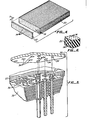
- an aniao- tropic elastomeric conductor material 22 of the present invention will find its greatest use in serving as an electrical interface between a semiconductor device 30 and a semiconductor support substrate 32.
- the semiconductor device 30 is of the type having a two-dimensional or planar array of electrical contact pads 34 on one face thereof.
- the support substrate 32 which is typically a multilayer connector board, is also characterized by a plurality of contact pads 36 arranged in a planar array. In general, the pattern in which the connector pads 34 are arranged on the semiconductor device 30 will correspond to that in which the contact pads 36 are arranged cn the support substrate 32.
- the anisotropic elastomeric conductor 22 is placed between the device 30 and the substrate 32, and the device 30 and substrate 32 brought together in proper alignment so that corresponding pads 34 and 36 are arranged on directly opposite sides of the conductor 22. By applying a certain minimal contact pressure between the device 30 and substrate 32, firm electrical contact is made between the contact pads and the intermediate conductors 12.
- sufficient electrically-conductive fibers are provided in the conductor 22 so that at least two fibers and preferably more than two fibers are intermediate each of the pairs of contact pads 34 and 36.
- the elastomeric conductors of the present invention may be used to provide for thermal coupling between a heat-generating device, typically an electronic device, and a heat sink.
- a heat-generating device typically an electronic device
- the conductive fibers 12 will generally have a relatively large diameter, typically on the order of 10 -2 cm.
- the elastomeric conductor of the present invention is particularly suitable for such applications since it will conform to both slight as well as mcre pronounced variations in the surface planarity of both the electronic device and the heat sink, thus assuring low thermal resistance between the two.
Landscapes
- Physics & Mathematics (AREA)
- Chemical & Material Sciences (AREA)
- Dispersion Chemistry (AREA)
- Spectroscopy & Molecular Physics (AREA)
- Engineering & Computer Science (AREA)
- Manufacturing & Machinery (AREA)
- Non-Insulated Conductors (AREA)
Applications Claiming Priority (2)
| Application Number | Priority Date | Filing Date | Title |
|---|---|---|---|
| US06/757,600 US4729166A (en) | 1985-07-22 | 1985-07-22 | Method of fabricating electrical connector for surface mounting |
| US757600 | 1986-07-22 |
Publications (3)
| Publication Number | Publication Date |
|---|---|
| EP0254598A2 true EP0254598A2 (de) | 1988-01-27 |
| EP0254598A3 EP0254598A3 (en) | 1989-11-23 |
| EP0254598B1 EP0254598B1 (de) | 1993-04-28 |
Family
ID=25048469
Family Applications (1)
| Application Number | Title | Priority Date | Filing Date |
|---|---|---|---|
| EP87400441A Expired - Lifetime EP0254598B1 (de) | 1985-07-22 | 1987-02-27 | Verfahren zum Herstellen eines elektrischen Verbinders für Oberflächenmontage |
Country Status (4)
| Country | Link |
|---|---|
| US (1) | US4729166A (de) |
| EP (1) | EP0254598B1 (de) |
| AU (1) | AU598236B2 (de) |
| DE (1) | DE3785619T2 (de) |
Cited By (1)
| Publication number | Priority date | Publication date | Assignee | Title |
|---|---|---|---|---|
| EP0341872A3 (de) * | 1988-05-09 | 1990-08-08 | AT&T Corp. | Steckverbinder mit hoher Dichte |
Families Citing this family (57)
| Publication number | Priority date | Publication date | Assignee | Title |
|---|---|---|---|---|
| US4918814A (en) * | 1984-12-20 | 1990-04-24 | Redmond John P | Process of making a layered elastomeric connector |
| US4820170A (en) * | 1984-12-20 | 1989-04-11 | Amp Incorporated | Layered elastomeric connector and process for its manufacture |
| US4754546A (en) * | 1985-07-22 | 1988-07-05 | Digital Equipment Corporation | Electrical connector for surface mounting and method of making thereof |
| US4835060A (en) * | 1987-09-16 | 1989-05-30 | Tecknit | Electrical connector |
| US4882657A (en) * | 1988-04-06 | 1989-11-21 | Ici Array Technology, Inc. | Pin grid array assembly |
| US5798780A (en) * | 1988-07-03 | 1998-08-25 | Canon Kabushiki Kaisha | Recording element driving unit having extra driving element to facilitate assembly and apparatus using same |
| EP0349959B1 (de) * | 1988-07-03 | 1997-12-10 | Canon Kabushiki Kaisha | Tintenstrahlaufzeichnungsvorrichtung |
| US5440240A (en) * | 1991-06-04 | 1995-08-08 | Micron Technology, Inc. | Z-axis interconnect for discrete die burn-in for nonpackaged die |
| JP2536676B2 (ja) * | 1990-07-30 | 1996-09-18 | 日本電気株式会社 | マイクロピン集合体及びその製造方法 |
| US5905382A (en) * | 1990-08-29 | 1999-05-18 | Micron Technology, Inc. | Universal wafer carrier for wafer level die burn-in |
| US7511520B2 (en) * | 1990-08-29 | 2009-03-31 | Micron Technology, Inc. | Universal wafer carrier for wafer level die burn-in |
| US6340894B1 (en) * | 1991-06-04 | 2002-01-22 | Micron Technology, Inc. | Semiconductor testing apparatus including substrate with contact members and conductive polymer interconnect |
| JPH0521544A (ja) * | 1991-07-12 | 1993-01-29 | Sumitomo Electric Ind Ltd | バンプ付き半導体素子の測定方法および測定装置 |
| US5585138A (en) * | 1991-07-30 | 1996-12-17 | Nec Corporation | Micropin array and production method thereof |
| US5543729A (en) * | 1991-09-10 | 1996-08-06 | Photon Dynamics, Inc. | Testing apparatus and connector for liquid crystal display substrates |
| DE4209097A1 (de) * | 1992-03-20 | 1993-09-23 | Manfred Dipl Ing Mueller | Universelles steckverbindersystem |
| US5483174A (en) * | 1992-06-10 | 1996-01-09 | Micron Technology, Inc. | Temporary connection of semiconductor die using optical alignment techniques |
| US5424652A (en) * | 1992-06-10 | 1995-06-13 | Micron Technology, Inc. | Method and apparatus for testing an unpackaged semiconductor die |
| US5395249A (en) * | 1993-06-01 | 1995-03-07 | Westinghouse Electric Corporation | Solder-free backplane connector |
| EP0779989A4 (de) * | 1994-09-09 | 1998-01-07 | Micromodule Systems Inc | Abtasten von schaltkreisen mit einem membranfühler |
| JPH10506459A (ja) * | 1994-09-09 | 1998-06-23 | マイクロモジュール・システムズ | 回路のメンブレンプローブ |
| KR100384265B1 (ko) * | 1994-10-28 | 2003-08-14 | 클리크 앤드 소파 홀딩스 인코포레이티드 | 프로그램가능한고집적전자검사장치 |
| US5605547A (en) * | 1995-03-27 | 1997-02-25 | Micron Technology, Inc. | Method and apparatus for mounting a component to a substrate using an anisotropic adhesive, a compressive cover film, and a conveyor |
| TW441227B (en) | 1995-05-26 | 2001-06-16 | E Tec Ag | Contact arrangement for detachably attaching an electric component, especially an integrated circuit to a printed circuit board |
| CH693478A5 (fr) | 1996-05-10 | 2003-08-15 | E Tec Ag | Socle de connexion de deux composants électriques. |
| US6103359A (en) * | 1996-05-22 | 2000-08-15 | Jsr Corporation | Process and apparatus for manufacturing an anisotropic conductor sheet and a magnetic mold piece for the same |
| US5695847A (en) * | 1996-07-10 | 1997-12-09 | Browne; James M. | Thermally conductive joining film |
| US6048599A (en) * | 1997-01-17 | 2000-04-11 | 3M Innovative Properties Company | Susceptor composite material patterned in neat polymer |
| DE19755792C2 (de) * | 1997-12-16 | 2001-05-17 | Titv Greiz | Textiles Flächengebilde aus mehreren miteinander verbundenen, teilweise elektrisch leitende Drähte/Fäden enthaltenden Gewebelagen |
| IL128997A (en) | 1999-03-15 | 2002-12-01 | Aprion Digital Ltd | Install electrical connection |
| US6351392B1 (en) * | 1999-10-05 | 2002-02-26 | Ironwood Electronics, Inc, | Offset array adapter |
| US6533589B1 (en) | 1999-10-14 | 2003-03-18 | Ironwood Electronics, Inc. | Packaged device adapter assembly |
| US6394820B1 (en) | 1999-10-14 | 2002-05-28 | Ironwood Electronics, Inc. | Packaged device adapter assembly and mounting apparatus |
| WO2003079495A1 (en) * | 2002-03-20 | 2003-09-25 | J.S.T. Mfg. Co., Ltd. | Flexible good conductive layer and anisotropic conductive sheet comprising same |
| WO2003079498A1 (fr) * | 2002-03-20 | 2003-09-25 | J.S.T. Mfg. Co., Ltd. | Bloc conducteur anisotrope et son procede de production |
| US20040050911A1 (en) * | 2002-09-18 | 2004-03-18 | Ho-Young Lee | Solder-fill and its manufacturing method for using semiconductor package and its application for mounting semiconductor chip on PCB |
| US6877993B2 (en) * | 2003-05-30 | 2005-04-12 | Ironwood Electronics, Inc. | Packaged device adapter assembly with alignment structure and methods regarding same |
| US8494195B2 (en) * | 2007-02-07 | 2013-07-23 | Starkey Laboratories, Inc. | Electrical contacts using conductive silicone in hearing assistance devices |
| US8385573B2 (en) | 2007-09-19 | 2013-02-26 | Starkey Laboratories, Inc. | System for hearing assistance device including receiver in the canal |
| WO2009049619A1 (en) * | 2007-10-16 | 2009-04-23 | Estron A/S | An electrical connector for a hearing device |
| CA2639555A1 (en) | 2008-08-11 | 2008-12-15 | Hyman Ngo | High definition litho applique and emblems |
| US8781141B2 (en) | 2008-08-27 | 2014-07-15 | Starkey Laboratories, Inc. | Modular connection assembly for a hearing assistance device |
| US8798299B1 (en) | 2008-12-31 | 2014-08-05 | Starkey Laboratories, Inc. | Magnetic shielding for communication device applications |
| US9002047B2 (en) * | 2009-07-23 | 2015-04-07 | Starkey Laboratories, Inc. | Method and apparatus for an insulated electromagnetic shield for use in hearing assistance devices |
| US8638965B2 (en) | 2010-07-14 | 2014-01-28 | Starkey Laboratories, Inc. | Receiver-in-canal hearing device cable connections |
| US9049526B2 (en) | 2011-03-19 | 2015-06-02 | Starkey Laboratories, Inc. | Compact programming block connector for hearing assistance devices |
| US9048565B2 (en) | 2013-06-12 | 2015-06-02 | Ironwood Electronics, Inc. | Adapter apparatus with deflectable element socket contacts |
| US9263817B2 (en) | 2013-06-12 | 2016-02-16 | Ironwood Electronics, Inc. | Adapter apparatus with suspended conductive elastomer interconnect |
| US9435855B2 (en) | 2013-11-19 | 2016-09-06 | Teradyne, Inc. | Interconnect for transmitting signals between a device and a tester |
| US9906879B2 (en) | 2013-11-27 | 2018-02-27 | Starkey Laboratories, Inc. | Solderless module connector for a hearing assistance device assembly |
| US9913052B2 (en) | 2013-11-27 | 2018-03-06 | Starkey Laboratories, Inc. | Solderless hearing assistance device assembly and method |
| US9594114B2 (en) | 2014-06-26 | 2017-03-14 | Teradyne, Inc. | Structure for transmitting signals in an application space between a device under test and test electronics |
| US9977052B2 (en) | 2016-10-04 | 2018-05-22 | Teradyne, Inc. | Test fixture |
| US9877404B1 (en) | 2017-01-27 | 2018-01-23 | Ironwood Electronics, Inc. | Adapter apparatus with socket contacts held in openings by holding structures |
| US10677815B2 (en) | 2018-06-08 | 2020-06-09 | Teradyne, Inc. | Test system having distributed resources |
| US11363746B2 (en) | 2019-09-06 | 2022-06-14 | Teradyne, Inc. | EMI shielding for a signal trace |
| US11862901B2 (en) | 2020-12-15 | 2024-01-02 | Teradyne, Inc. | Interposer |
Family Cites Families (30)
| Publication number | Priority date | Publication date | Assignee | Title |
|---|---|---|---|---|
| US2425294A (en) * | 1944-12-18 | 1947-08-12 | John T Morgan | Method of making insulated multiconductor structures |
| US3128214A (en) * | 1959-04-06 | 1964-04-07 | Ling Temco Vought Inc | Method of making multiconductor cable |
| US3014980A (en) * | 1959-04-13 | 1961-12-26 | Gen Electric | Insulation systems |
| US3264403A (en) * | 1963-10-15 | 1966-08-02 | Eldre Components | Electrical bus bar with non-adhering plastic inserts |
| DE1289300B (de) * | 1967-02-23 | 1969-02-13 | Rost & Co H | Gewebeeinlage fuer einen Foerdergurt oder Treibriemen |
| US3547718A (en) * | 1967-05-18 | 1970-12-15 | Rogers Corp | Method of making flat flexible electrical cables |
| US3816575A (en) * | 1968-07-22 | 1974-06-11 | Lion Fat Oil Co Ltd | Method for preparing a porous thermoplastic resin sheet |
| GB1387587A (en) * | 1971-07-22 | 1975-03-19 | Plessey Co Ltd | Electrical interconnectors and connector assemblies |
| US3710303A (en) * | 1971-09-13 | 1973-01-09 | Rca Corp | Edge connector |
| JPS5187787A (en) * | 1975-01-31 | 1976-07-31 | Shinetsu Polymer Co | Intaa konekutaa |
| US3982320A (en) * | 1975-02-05 | 1976-09-28 | Technical Wire Products, Inc. | Method of making electrically conductive connector |
| US4003621A (en) * | 1975-06-16 | 1977-01-18 | Technical Wire Products, Inc. | Electrical connector employing conductive rectilinear elements |
| US4217155A (en) * | 1975-09-12 | 1980-08-12 | Amp Incorporated | Multi-pair cable having low crosstalk |
| JPS5265892A (en) * | 1975-11-26 | 1977-05-31 | Shinetsu Polymer Co | Nonnisotropic conductiveesheet type composite materials and method of manufacture thereof |
| JPS583343B2 (ja) * | 1976-06-14 | 1983-01-20 | 信越ポリマ−株式会社 | インタ−コネクタ− |
| GB1553575A (en) * | 1976-07-21 | 1979-09-26 | Tekdata Ltd | Electrical conductor ribbon and the manufacture thereof |
| US4201435A (en) * | 1976-07-26 | 1980-05-06 | Shin-Etsu Polymer Co. Ltd. | Interconnectors |
| US4096006A (en) * | 1976-09-22 | 1978-06-20 | Spectra-Strip Corporation | Method and apparatus for making twisted pair multi-conductor ribbon cable with intermittent straight sections |
| JPS5915376B2 (ja) * | 1977-10-18 | 1984-04-09 | 信越ポリマ−株式会社 | 電子回路部品 |
| JPS5482699A (en) * | 1977-12-15 | 1979-07-02 | Shinetsu Polymer Co | Pressure sensitive resistance element |
| JPS5555985U (de) * | 1978-10-12 | 1980-04-16 | ||
| JPS5826381B2 (ja) * | 1979-04-28 | 1983-06-02 | 信越ポリマ−株式会社 | 電磁気シ−ルドガスケットおよびその製造方法 |
| US4252391A (en) * | 1979-06-19 | 1981-02-24 | Shin-Etsu Polymer Co., Ltd. | Anisotropically pressure-sensitive electroconductive composite sheets and method for the preparation thereof |
| JPS568081U (de) * | 1979-06-29 | 1981-01-23 | ||
| JPS6038809B2 (ja) * | 1979-11-20 | 1985-09-03 | 信越ポリマ−株式会社 | 異方導電性を有するエラスチツク構造体の製造方法 |
| JPS5740874A (en) * | 1980-08-22 | 1982-03-06 | Shinetsu Polymer Co | Pressure contact holding type connector |
| US4449774A (en) * | 1981-02-05 | 1984-05-22 | Shin-Etsu Polymer Co., Ltd. | Electroconductive rubbery member and elastic connector therewith |
| US4442317A (en) * | 1981-09-14 | 1984-04-10 | Sun-Flex Company, Inc. | Coordinate sensing device |
| US4437718A (en) * | 1981-12-17 | 1984-03-20 | Motorola Inc. | Non-hermetically sealed stackable chip carrier package |
| GB8502203D0 (en) * | 1985-01-29 | 1985-02-27 | Univ Strathclyde | Elastomeric electro-conductive materials |
-
1985
- 1985-07-22 US US06/757,600 patent/US4729166A/en not_active Expired - Lifetime
-
1987
- 1987-02-25 AU AU69249/87A patent/AU598236B2/en not_active Ceased
- 1987-02-27 EP EP87400441A patent/EP0254598B1/de not_active Expired - Lifetime
- 1987-02-27 DE DE87400441T patent/DE3785619T2/de not_active Expired - Lifetime
Cited By (1)
| Publication number | Priority date | Publication date | Assignee | Title |
|---|---|---|---|---|
| EP0341872A3 (de) * | 1988-05-09 | 1990-08-08 | AT&T Corp. | Steckverbinder mit hoher Dichte |
Also Published As
| Publication number | Publication date |
|---|---|
| AU6924987A (en) | 1988-09-01 |
| EP0254598B1 (de) | 1993-04-28 |
| DE3785619D1 (de) | 1993-06-03 |
| AU598236B2 (en) | 1990-06-21 |
| US4729166A (en) | 1988-03-08 |
| EP0254598A3 (en) | 1989-11-23 |
| DE3785619T2 (de) | 1993-12-23 |
Similar Documents
| Publication | Publication Date | Title |
|---|---|---|
| US4729166A (en) | Method of fabricating electrical connector for surface mounting | |
| EP0238410B1 (de) | Elektrischer Verbinder für Oberflächenmontage und Verfahren zu dessen Herstellung | |
| US4778950A (en) | Anisotropic elastomeric interconnecting system | |
| US4954873A (en) | Electrical connector for surface mounting | |
| US4737112A (en) | Anisotropically conductive composite medium | |
| US5890915A (en) | Electrical and thermal conducting structure with resilient conducting paths | |
| US5624268A (en) | Electrical connectors using anisotropic conductive films | |
| JP3038859B2 (ja) | 異方導電性シート | |
| US3541222A (en) | Connector screen for interconnecting adjacent surfaces of laminar circuits and method of making | |
| CN1386302A (zh) | 承座格距阵列连接器用的载台 | |
| DE3783266T2 (de) | Loesbares montierungssystem fuer halbleiter auf einem leitenden substrat. | |
| CN1057641C (zh) | 低电阻转接器及其制备方法 | |
| JP4041619B2 (ja) | インターコネクタの製造方法 | |
| US20050194697A1 (en) | Anisotropic conductive sheet and manufacture thereof | |
| CA1269728A (en) | Method of fabricating electrical connector for surface mounting | |
| JPH0574512A (ja) | 電気接続用コネクタ | |
| JPH0239069B2 (de) | ||
| JPH0197382A (ja) | 異方導電性コネクターおよびその製造方法 | |
| JP2003017158A (ja) | 圧接型シートコネクタ及びその製造方法 | |
| Xu et al. | Z-Axis anisotropic electrical conductor films in adhesive and standalone forms for electrical interconnection | |
| JP2004079277A (ja) | 電気コネクタ | |
| JPH0218554B2 (de) | ||
| JPH03216972A (ja) | 低抵抗エラスチックコネクター及びその製造方法 | |
| JPH025376A (ja) | 低抵抗エラスチックコネクター |
Legal Events
| Date | Code | Title | Description |
|---|---|---|---|
| PUAI | Public reference made under article 153(3) epc to a published international application that has entered the european phase |
Free format text: ORIGINAL CODE: 0009012 |
|
| AK | Designated contracting states |
Kind code of ref document: A2 Designated state(s): BE CH DE FR GB IT LI NL |
|
| PUAL | Search report despatched |
Free format text: ORIGINAL CODE: 0009013 |
|
| AK | Designated contracting states |
Kind code of ref document: A3 Designated state(s): BE CH DE FR GB IT LI NL |
|
| 17P | Request for examination filed |
Effective date: 19900507 |
|
| 17Q | First examination report despatched |
Effective date: 19900814 |
|
| GRAA | (expected) grant |
Free format text: ORIGINAL CODE: 0009210 |
|
| AK | Designated contracting states |
Kind code of ref document: B1 Designated state(s): BE CH DE FR GB IT LI NL |
|
| PG25 | Lapsed in a contracting state [announced via postgrant information from national office to epo] |
Ref country code: NL Effective date: 19930428 Ref country code: LI Effective date: 19930428 Ref country code: CH Effective date: 19930428 Ref country code: BE Effective date: 19930428 |
|
| REF | Corresponds to: |
Ref document number: 3785619 Country of ref document: DE Date of ref document: 19930603 |
|
| ITF | It: translation for a ep patent filed | ||
| ET | Fr: translation filed | ||
| REG | Reference to a national code |
Ref country code: CH Ref legal event code: PL |
|
| NLV1 | Nl: lapsed or annulled due to failure to fulfill the requirements of art. 29p and 29m of the patents act | ||
| PG25 | Lapsed in a contracting state [announced via postgrant information from national office to epo] |
Ref country code: GB Effective date: 19940227 |
|
| ITTA | It: last paid annual fee | ||
| PLBE | No opposition filed within time limit |
Free format text: ORIGINAL CODE: 0009261 |
|
| STAA | Information on the status of an ep patent application or granted ep patent |
Free format text: STATUS: NO OPPOSITION FILED WITHIN TIME LIMIT |
|
| 26N | No opposition filed | ||
| GBPC | Gb: european patent ceased through non-payment of renewal fee |
Effective date: 19940227 |
|
| PG25 | Lapsed in a contracting state [announced via postgrant information from national office to epo] |
Ref country code: FR Effective date: 19941031 |
|
| PG25 | Lapsed in a contracting state [announced via postgrant information from national office to epo] |
Ref country code: DE Effective date: 19941101 |
|
| REG | Reference to a national code |
Ref country code: FR Ref legal event code: ST |
|
| PG25 | Lapsed in a contracting state [announced via postgrant information from national office to epo] |
Ref country code: IT Free format text: LAPSE BECAUSE OF NON-PAYMENT OF DUE FEES Effective date: 20050227 |