EP0254017A2 - Geeichtes automatisches Prüfsystem - Google Patents
Geeichtes automatisches Prüfsystem Download PDFInfo
- Publication number
- EP0254017A2 EP0254017A2 EP87108483A EP87108483A EP0254017A2 EP 0254017 A2 EP0254017 A2 EP 0254017A2 EP 87108483 A EP87108483 A EP 87108483A EP 87108483 A EP87108483 A EP 87108483A EP 0254017 A2 EP0254017 A2 EP 0254017A2
- Authority
- EP
- European Patent Office
- Prior art keywords
- test
- codes
- digital
- test system
- automatic
- Prior art date
- Legal status (The legal status is an assumption and is not a legal conclusion. Google has not performed a legal analysis and makes no representation as to the accuracy of the status listed.)
- Granted
Links
Images


Classifications
-
- G—PHYSICS
- G01—MEASURING; TESTING
- G01R—MEASURING ELECTRIC VARIABLES; MEASURING MAGNETIC VARIABLES
- G01R31/00—Arrangements for testing electric properties; Arrangements for locating electric faults; Arrangements for electrical testing characterised by what is being tested not provided for elsewhere
- G01R31/28—Testing of electronic circuits, e.g. by signal tracer
- G01R31/317—Testing of digital circuits
- G01R31/3181—Functional testing
- G01R31/319—Tester hardware, i.e. output processing circuits
- G01R31/31903—Tester hardware, i.e. output processing circuits tester configuration
- G01R31/31908—Tester set-up, e.g. configuring the tester to the device under test [DUT], down loading test patterns
- G01R31/3191—Calibration
Definitions
- the following invention relates to an automatic test system for testing electronic devices and having a calibration feature for ensuring the accurate generation of test signals for a device under test.
- test system for VLSI devices presents special engineering problems.
- testers with as many as 256 I/O channels, 50 MHz clock and data rates, subnanosecond timing resolution and large test pattern memories associated with each of the 256 I/O channels.
- test systems that satisfy these criteria are extremely expensive. This is due to the fact that the best architecture for such testers requires redundant sets of tester electronics, one for each output pin of the tester. This is referred to as tester-per-pin architecture.
- test circuitry is desirable because with it the problems of multiplexing and cabling, that would otherwise arise with shared test circuitry, are avoided and the test circuits can be located physically adjacent each input/output pin in close proximity with the device under test. Moreover, complex test patterns may be generated since each of the input/output pin circuits are independent and have independent timing generation and output pattern acquisition.
- the problem with tester-per-pin architecture is that the redundancy of the pin circuits makes the test instrument very expensive.
- the pin electronics circuits must include precision components which ensure accuracy of all relevant electrical parameters. Duplicating these types of circuits results in a considerable increase in the overall costs of the unit.
- the present invention provides an automatic test system which has the flexibility of tester-per-pin architecture but which can be produced at a relatively modest cost.
- a calibrated automatic test system for testing electronic devices comprises a programmable test station which includes a test head having a plurality of input/output pins for connection to a device under test.
- CMOS integrated pin circuits are provided for each of the I/O pins for generating the signals needed to stimulate the device under test.
- An external calibration unit which is selectively connectable to the test head receives test signals from the CMOS integrated pin electronics circuits and derives from those test signals error correction signals which may be used to calibrate the CMOS IC's in each of the individual pin electronics circuits.
- tester-per-pin architecture is utilized in the present system, it is less expensive because of the incorporation of monolithic CMOS integrated circuits for each of the pin electronics circuits.
- CMOS IC's would ordinarily subject the tester to a host of inaccuracies due to the variations in circuit parameters that result from the manufacturing processes used to make the IC's.
- the external calibration unit solves this problem by measuring the test signals generated by each of the pin electronic circuits, stores those signals in a memory, and utilizes the signals in the memory to provide error correction factors for calibrating the IC's.
- the test unit which may be under the control of a host computer, generates test signals through digital function codes which are provided to each of the pin electronic circuits.
- the pin electronic circuits are responsive to error correction memory circuits which provide error correction signals derived by the external calibration unit for altering the test function digital codes thereby producing calibrated test signals at the output of each pin electronics circuit.
- the external calibration unit may be portable and thus may be used with several test stations, and may include an X-Y positioning apparatus for making selective connection with each I/O pin of the test head for calibrating each pin electronics circuit in turn.
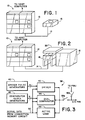
- An automatic test unit 10 includes a test station 12 which includes programmable test circuitry under the control of a host computer (not shown) for generating digital test function codes over a connecting cable 14 to a test head 16.
- the test head 16 may be loaded with a device under test (not shown) such as a VLSI chip which may have as many as 256 input/output lines.
- a device under test such as a VLSI chip which may have as many as 256 input/output lines.
- Each I/O line is connected to the device under test by a pin (not shown) and each of the pins includes a pin electronics circuit 38 (refer to FIG. 3) to provide test signals to the device under test in response to digital test function codes generated by the test station 12.
- the automatic test system includes an external calibration unit 18 which may include an X-Y positioning device 20 which may be positioned to connect to various pins of the test head 16.
- the positioning device may include a probe head 36 which may move in two dimensions as shown by the arrows in FIG. 2b.
- the external calibration unit 18 is shown in more detail in FIG. 2b, and comprises several modules including a time measurement circuit 20, pulse generator 22, programmable counter 24, volt meters and ammeters 26, precision resistances 28, and precision voltage sources 30.
- a series of relays 34 selectively connects the modules of the external calibration unit 18 to the coaxial cable 32 except a memory unit 31 which is internally connected to the other circuits.
- the external calibration unit 18, with its associated X-Y positioning device 20, may be portable and may be mounted in a cart or rack having wheels (not shown) so that it can be moved about from one test unit 10 to another. This provides for additional economy of the system because only one external calibration unit 18 may be needed for a plurality of test units 10.
- FIG. 3 A block schematic diagram of the pin electronics circuit 38 for one of the I/O pins of test head 16 is shown in FIG. 3.
- the circuits represented by the block diagram of FIG. 3 may be contained on two monolithic CMOS integrated circuit chips. These must be small-geometry CMOS chips to fit within test head 16 adjacent each of the I/O pins, and, as a consequence, exhibit large variations in performance characteristics at the speeds at which test signals must be transmitted and acquired for VLSI testing. These speeds typically approach 50 MHz. Thus, while the pin electronics circuits 38 may be placed adjacent the pins of the test head 16, they must be calibrated if the system is to remain accurate.
- the CMOS pin electronics circuit 38 includes driver pulse generators 40 which provide pulses for a driver circuit 42.
- the driver 42 provides timed output pulses which stimulate the device under test. Signals from the device under test are acquired by a dual comparator 44 and an active load circuit 46.
- the dual comparator 44 is controlled by comparator clock generators 48.
- the driver 42, the dual comparator 44 and the active load 46 are controlled by digital test function codes from incoming serial data line 50.
- Serial data line 50 is connected to the output of a correction memory circuit as will be explained below.
- a pair of relays 52a and 52b connect either the pin electronics circuit 38 or a parametric measurement unit (not shown) to one of the input/output pins of test head 16.
- the parametric measurement unit is a DC measuring device which may be shared among a plurality of pin electronics circuits 38 and which may be used to measure various DC characteristics of a device under test.
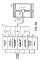
- the driver pulse generators 40 include four output lines which are seen in FIG. 4 as input lines labelled "driver high pulse,” “driver low pulse,” “driver off pulse,” and “driver on pulse.” These lines are connected to pulse placement circuits 54, 56, 58 and 60, respectively. Pulse placement circuits 54 and 56 provide inputs to flip flop 62, and pulse placement circuits 58 and 60 provide inputs to flip flop 64. The outputs of flip flops 62 and 64 are provided to AND gates 66 and 68. The output of AND gates 66 and 68 are connected to transmission gates 70 and 72 respectively, which gate either a driver high voltage rail 71 or a driver low voltage rail 73 through relay 52a.
- the driver circuit 42 may thus have three states: it may provide a logical high signal, a logical low signal or it may be turned off.
- the timing of the leading edges of the driver circuits 42 in all of the pin electronics 38 may be critical. For example, it may be desirable to time all of the leading edges of pulses produced by the driver circuits 42 so that they all occur within a certain number of nanoseconds relative to a reference determined by a master clock located in test station 12 or in the host computer. This process is known as deskewing the input drivers and makes it possible to generate test pulses that arrive simultaneously on all input pins of interest in the test head 16.
- the pulse placement circuits 54, 56, 58 and 60 are arranged so as to provide variable delays which may be adjusted by an 8-bit digital signal.
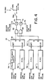
- the circuit for implementing driver pulse timing adjustability is shown in FIG. 5.
- the pulse placement circuit shown in FIG. 5 includes a plurality of multiplexers 74a through 74h. Each one of the multiplexers 74a-74h is connected to one of the lines of an 8-bit shift register 75. The lines from shift register 75 are connected to the SET inputs of multiplexers 74a-74h and choose, depending upon the state of the line, that is, whether a logical high or a logical low, either input A or B.
- the B input on each of the multiplexers 74a-74h is generally configured to provide more delay to the signal input.
- a capacitor connected in parallel with the B input provides additional delay.
- pluralities of buffer amplifiers provide increased delay for the B input as opposed to the A input.
- the digital code loaded into shift register 75 controls the choice at each of the multiplexers 74a-74h of the A or B input and thereby chooses the amount of delay through the pulse placement circuit 54.
- the "serial data in" line connected to the shift register 75 is from the output of an error correction circuit which is shown in FIG. 6.
- the error correction circuit such as circuit 76 shown in block diagram form in FIG. 6, includes an output for each of the pin electronic circuits such as circuit 38 shown in FIG. 3.
- an error correction memory circuit includes a random access memory 77 which is configured, by way of example only, as a 32k x 8 random access memory.
- the memory 77 would be configured as a 32k x 256 RAM.
- Each data I/O line of RAM 77 is connected to a data output circuit 78.
- Each data output circuit 78 includes a multiplexer 79 having its B input connected to the data I/O port of RAM 77 and its A input line connected to a serial data input line 80.
- the serial data line 80 is also connected to an 8-bit shift register 81 which has an output leading to a tristateable buffer amplifier 82.
- the tristateable buffer amplifier 82 is also connected to the SET input of multiplexer 79 and to a node between the data I/O outputs of RAM 77 and the B input of multiplexer 79.
- Connected to the address lines of RAM 77 are a 3-bit counter 83, an 8-bit shift/count register, and a 4-bit shift register 85.
- the 4-bit shift register 85 has an input which provides a serial function code
- the 8-bit shift/count register has a shift/count input line controlling the function of the register 84, that is, whether it functions as a shift register or as a counter.
- the purpose of the RAM 77 is to store corrected test function codes in address locations that may be accessed by nominal test function codes generated by the test modules included at test station 12.
- the test function codes may instruct the pin electronic circuits 38 to perform various test functions such as, for example, generating a test pulse at a time relative to some standard. Because of the variations in performance of the CMOS integrated circuits which contain the pin electronics circuits 38, the actual timing of such a pulse called for by a specific test function code, may not occur at the desired time.
- the correction memory circuit 76 provides correct test function codes which may be substituted for the function codes generated from the test station 12 so that the performance of the pin electronics circuits 38 corresponds to the actual desired performance.
- the external calibration unit 18 is positioned over the test head 16 as shown in FIG. 2.
- the X-Y positioning unit 20 is connected to each I/O pin of the test head 16 in turn, and measurements are taken which record the actual performance of each of the pin electronics circuits 38 in response to test function codes generated from the test station 12.
- the timing of the driver pulses from driver circuit 42 is controlled by the pulse placement circuit 54.
- This circuit is controlled in turn by an 8-bit shift register 75 which receives a test function code from test station 12. Since shift register 75 is an 8-bit register, there may be as many as 256 possible values for the timing of the leading edge of drive pulses for drive circuit 42.
- the host computer connected to each test station 12 may determine which test functions are to be implemented and analyzes the test data that is received, and may control the operation of the external calibration unit 18.
- the test station 12 initiates a test of the driver leading edge timing and proceeds to provide the pin electronics circuit 38 with each of the 256 possible values for the timing of the output of the driver circuit 42.
- the RAM 77 in the correction memory circuit 76 is turned off and the output of the circuits 78 comprises serial data from the serial data input line 80.
- the calibration unit 18 records the actual timing data resulting from the 256 test function codes in its memory 31.
- the host computer determines a desired data value which may, for example, be the timing of a pulse relative to a reference standard. It searches the memory 31 for the data entry that most closely approximates the desired performance of the circuit. Once this data entry has been looked up in the memory 31, its test function code is determined and that code is transferred to a location in RAM 77 which has an address which may be accessed by the nominal test function codes produced by the test station 12.
- the memory 31 may store all 256 possible values for the timing of the leading edge of a driver pulse relative to a reference. If the drivers 42 were to be deskewed so that all drivers 42 timed the leading edges of their output pulses to occur 10 nanoseconds after a predetermined clock or reference, the host computer would perform a table lookup in the memory 31 for a data value that represented most closely the desired 10 nanosecond timing relationship. The function code that produced this data value would then be stored in the error correction RAM 77.
- This data is written into the RAM 77 by turning off the data I/O lines and loading the data into 8-bit shift register 81.
- the data is placed in the memory on one of the data I/O lines through tristateable buffer 82.
- the "memory write" line of RAM 77 is enabled, and the "use corrected data” line on input OE is turned off which inhibits the output of the data I/O lines.
- the function code that produced the 10 nanosecond timing is placed in an address location in the RAM 77 where it will be accessed by the function code from test station 12 that nominally produces the 10 nanosecond timing relationship. When this has been done for all test functions of interest, RAM 77 will contain calibrated test function codes which may be substituted for incoming nominal test function codes.
- the external calibration unit 18 may be removed from the test head 16.
- a function code entering on serial data line 80 will enter 8-bit shift/count register 84.
- a serial function code determines which one of 16 possible test function types is being called up out of memory.
- the output of the shift/count register 84 will be an address location which contains the calibrated test function code which, in the present example, will cause the pin electronics circuits 38 to provide the desired pulse timing for the driver circuits 42.
- the corrected function code will therefore be substituted for the nominal test function code entering on serial data line 80.
- the corrected test function code will be serially loaded into multipexer 79 one bit at a time by 3-bit counter 83.
- the data I/O lines of RAM 77 are turned on by the "use corrected data" input, which also turns off tristateable buffers 82 and selects line B of multiplexers 79.
- the substituted 8-bit test function code on the serial data output line forms the serial data input to the 8-bit shift register 75 (refer to FIG. 5) which, as explained above, sets the timing for the pulses of driver circuit 42 in each of the pin electronic circuits 38 (refer to FIG. 3).
- the invention has thus been explained by reference to an example in the pin electronics circuits 38 involving the timing of the leading edge of output pulses from driver circuits 42. It should be understood, however, that the other circuits in the pin electronics circuits 38, such as the dual comparators 44 and the active loads 46, also require calibration and thus have inputs from the serial data line 50 from the correction memory unit 76 shown in FIG. 6. For example, there are offset and linearity errors that are introduced by digital to analog (DAC) circuits in dual comparator 44. The voltage produced by the DACs also depends upon digital test function codes generated in the test station 12. Similarly, the active load circuits 46 are used to sink or source current to a device under test and depend upon other DAC voltages in their respective circuits which in turn depend upon digital codes at the input of the DACs.
- DAC digital to analog
- the invention has been described as a calibration unit for monolithic CMOS integrated circuits which are used as pin electronics circuits, the invention is applicable to any type of electronic circuit which inherently lacks the accuracy required for VLSI testing at speeds in the 50 MHz range.
- the calibration system of the instant invention is applicable to any other type of electronic circuit which requires calibration for accurate testing, and there is no intent to limit the invention described herein solely to CMOS integrated circuits.
Applications Claiming Priority (2)
| Application Number | Priority Date | Filing Date | Title |
|---|---|---|---|
| US888906 | 1986-07-22 | ||
| US06/888,906 US4724378A (en) | 1986-07-22 | 1986-07-22 | Calibrated automatic test system |
Publications (3)
| Publication Number | Publication Date |
|---|---|
| EP0254017A2 true EP0254017A2 (de) | 1988-01-27 |
| EP0254017A3 EP0254017A3 (en) | 1989-09-27 |
| EP0254017B1 EP0254017B1 (de) | 1994-09-28 |
Family
ID=25394143
Family Applications (1)
| Application Number | Title | Priority Date | Filing Date |
|---|---|---|---|
| EP87108483A Expired - Lifetime EP0254017B1 (de) | 1986-07-22 | 1987-06-12 | Geeichtes automatisches Prüfsystem |
Country Status (5)
| Country | Link |
|---|---|
| US (1) | US4724378A (de) |
| EP (1) | EP0254017B1 (de) |
| JP (1) | JPH0664124B2 (de) |
| CA (1) | CA1273678A (de) |
| DE (1) | DE3750597T2 (de) |
Cited By (4)
| Publication number | Priority date | Publication date | Assignee | Title |
|---|---|---|---|---|
| EP0547682A2 (de) * | 1991-12-18 | 1993-06-23 | International Business Machines Corporation | Speichertestssystem mit algorithmischer Testdatenerzeugung |
| WO1997005498A1 (en) * | 1995-08-01 | 1997-02-13 | Teradyne, Inc. | Low cost cmos tester |
| CN1804648B (zh) * | 2005-01-14 | 2010-06-23 | 惠瑞捷(新加坡)私人有限公司 | 自动测试装置校准因子的递增产生 |
| WO2013130621A1 (en) * | 2012-02-29 | 2013-09-06 | Qualcomm Incorporated | Apparatus and method for precise calibration of electronic components |
Families Citing this family (36)
| Publication number | Priority date | Publication date | Assignee | Title |
|---|---|---|---|---|
| FR2604260B1 (fr) * | 1986-09-19 | 1988-12-30 | Draxy Sarl | Testeur de circuits electroniques |
| USRE36063E (en) * | 1987-02-09 | 1999-01-26 | Teradyne, Inc. | Timing generator with edge generators, utilizing programmable delays, providing synchronized timing signals at non-integer multiples of a clock signal |
| US4837764A (en) * | 1987-03-26 | 1989-06-06 | Bunker Ramo Corporation | Programmable apparatus and method for testing computer peripherals |
| US5369593A (en) * | 1989-05-31 | 1994-11-29 | Synopsys Inc. | System for and method of connecting a hardware modeling element to a hardware modeling system |
| US5353243A (en) * | 1989-05-31 | 1994-10-04 | Synopsys Inc. | Hardware modeling system and method of use |
| JPH0361588U (de) * | 1989-10-23 | 1991-06-17 | ||
| US5127011A (en) * | 1990-01-12 | 1992-06-30 | International Business Machines Corporation | Per-pin integrated circuit test system having n-bit interface |
| JP2716288B2 (ja) * | 1991-05-31 | 1998-02-18 | 山形日本電気株式会社 | 半導体回路試験方式 |
| US5414712A (en) * | 1991-07-23 | 1995-05-09 | Progressive Computing, Inc. | Method for transmitting data using a communication interface box |
| US5471136A (en) * | 1991-07-24 | 1995-11-28 | Genrad Limited | Test system for calculating the propagation delays in signal paths leading to a plurality of pins associated with a circuit |
| DE69333571T2 (de) * | 1992-07-27 | 2005-08-04 | Credence Systems Corp., Fremont | Gerät zur automatischen prüfung von komplexen vorrichtungen |
| US5412664A (en) * | 1992-12-23 | 1995-05-02 | Motorola, Inc. | Integrated circuit and method of testing |
| US5377202A (en) * | 1993-05-03 | 1994-12-27 | Raytheon Company | Method and apparatus for limiting pin driver offset voltages |
| US5842155A (en) * | 1993-05-03 | 1998-11-24 | Fairchild Semiconductor Corp. | Method and apparatus for adjusting pin driver charging and discharging current |
| CA2127192C (en) * | 1993-07-01 | 1999-09-07 | Alan Brent Hussey | Shaping ate bursts, particularly in gallium arsenide |
| US5416512A (en) * | 1993-12-23 | 1995-05-16 | International Business Machines Corporation | Automatic threshold level structure for calibrating an inspection tool |
| US5673295A (en) * | 1995-04-13 | 1997-09-30 | Synopsis, Incorporated | Method and apparatus for generating and synchronizing a plurality of digital signals |
| US6374379B1 (en) * | 1999-02-05 | 2002-04-16 | Teradyne, Inc. | Low-cost configuration for monitoring and controlling parametric measurement units in automatic test equipment |
| US6377901B1 (en) * | 1999-03-01 | 2002-04-23 | Agilent Technologies, Inc. | Method and apparatus for adaptively learning test measurement delays on an individual device test for reducing total device test time |
| DE10141025B4 (de) * | 2001-08-22 | 2007-05-24 | Infineon Technologies Ag | Verfahren zum Testen von Wafern unter Verwendung eines Kalibrierwafers und zugehöriger Kalibriewafer |
| US20040199842A1 (en) * | 2003-04-04 | 2004-10-07 | Sartschev Ronald A. | Test system with high accuracy time measurement system |
| US20050015122A1 (en) * | 2003-06-03 | 2005-01-20 | Mott Christopher Grey | System and method for control of a subject's circadian cycle |
| US7099599B2 (en) * | 2003-08-15 | 2006-08-29 | Static Control Components, Inc. | System and method for port testing and configuration |
| US7519877B2 (en) * | 2004-08-10 | 2009-04-14 | Micron Technology, Inc. | Memory with test mode output |
| DE102004057772B3 (de) * | 2004-11-30 | 2006-05-24 | Infineon Technologies Ag | Einsetzbare Kalibriervorrichtung |
| WO2008144908A1 (en) * | 2007-05-29 | 2008-12-04 | Christopher Mott | Methods and systems for circadian physiology predictions |
| US8781796B2 (en) | 2007-10-25 | 2014-07-15 | Trustees Of The Univ. Of Pennsylvania | Systems and methods for individualized alertness predictions |
| US7768255B2 (en) * | 2008-08-28 | 2010-08-03 | Advantest Corporation | Interconnection substrate, skew measurement method, and test apparatus |
| US8794976B2 (en) * | 2009-05-07 | 2014-08-05 | Trustees Of The Univ. Of Pennsylvania | Systems and methods for evaluating neurobehavioural performance from reaction time tests |
| US8521439B2 (en) * | 2009-05-08 | 2013-08-27 | Pulsar Informatics, Inc. | Method of using a calibration system to generate a latency value |
| US9164159B2 (en) | 2012-12-14 | 2015-10-20 | Apple Inc. | Methods for validating radio-frequency test stations |
| WO2015069263A1 (en) * | 2013-11-07 | 2015-05-14 | Advantest Corporation | A method and apparatus for improving differential direct current ("dc") measurement accuracy |
| US9494671B2 (en) * | 2013-11-08 | 2016-11-15 | Advantest Corporation | Method and apparatus for improving differential direct (DC) measurement accuracy |
| KR102098309B1 (ko) * | 2018-07-24 | 2020-04-08 | 주식회사 한국계측기기연구센터 | Gps 기반 속도계 교정시스템 및 교정 방법 |
| CN114200370A (zh) * | 2020-09-18 | 2022-03-18 | 中国科学院微电子研究所 | 一种测试设备及集成电路测试方法 |
| CN112752097B (zh) * | 2020-12-30 | 2023-05-26 | 长春长光辰芯微电子股份有限公司 | 一种cmos图像传感器的测试方法和系统 |
Citations (2)
| Publication number | Priority date | Publication date | Assignee | Title |
|---|---|---|---|---|
| JPS57111472A (en) * | 1980-12-29 | 1982-07-10 | Advantest Corp | Logical-circuit testing device |
| EP0165865A2 (de) * | 1984-06-14 | 1985-12-27 | Fairchild Semiconductor Corporation | Verfahren und Gerät zum Prüfen von integrierten Schaltungen |
Family Cites Families (7)
| Publication number | Priority date | Publication date | Assignee | Title |
|---|---|---|---|---|
| US4099240A (en) * | 1977-01-14 | 1978-07-04 | Hewlett-Packard Company | Method and apparatus for programmable and remote numeric control and calibration of electronic instrumentation |
| US4125763A (en) * | 1977-07-15 | 1978-11-14 | Fluke Trendar Corporation | Automatic tester for microprocessor board |
| US4354268A (en) * | 1980-04-03 | 1982-10-12 | Santek, Inc. | Intelligent test head for automatic test system |
| US4590422A (en) * | 1981-07-30 | 1986-05-20 | Pacific Western Systems, Inc. | Automatic wafer prober having a probe scrub routine |
| US4635256A (en) * | 1983-08-01 | 1987-01-06 | Fairchild Semiconductor Corporation | Formatter for high speed test system |
| US4637020A (en) * | 1983-08-01 | 1987-01-13 | Fairchild Semiconductor Corporation | Method and apparatus for monitoring automated testing of electronic circuits |
| JPS61286768A (ja) * | 1985-06-13 | 1986-12-17 | Hitachi Ltd | テスト装置 |
-
1986
- 1986-07-22 US US06/888,906 patent/US4724378A/en not_active Expired - Lifetime
-
1987
- 1987-05-28 CA CA000538287A patent/CA1273678A/en not_active Expired - Fee Related
- 1987-06-12 EP EP87108483A patent/EP0254017B1/de not_active Expired - Lifetime
- 1987-06-12 DE DE3750597T patent/DE3750597T2/de not_active Expired - Fee Related
- 1987-07-20 JP JP62180901A patent/JPH0664124B2/ja not_active Expired - Lifetime
Patent Citations (2)
| Publication number | Priority date | Publication date | Assignee | Title |
|---|---|---|---|---|
| JPS57111472A (en) * | 1980-12-29 | 1982-07-10 | Advantest Corp | Logical-circuit testing device |
| EP0165865A2 (de) * | 1984-06-14 | 1985-12-27 | Fairchild Semiconductor Corporation | Verfahren und Gerät zum Prüfen von integrierten Schaltungen |
Non-Patent Citations (4)
| Title |
|---|
| ELECTRONIC DESIGN, vol. 34, no. 17, 24th July 1986, pages 51-54, Hasbrouck Heights, US; B. MILNE: "Pin electronics tailors tester to CMOS ASICs" * |
| IEEE - INTERNATIONAL TEST CONFERENCE 1985 PROCEEDINGS, 19th - 21st November 1985, pages 191-202, IEEE, New York, US; J. HEALY et al.: "A method of reducing ATE system error components and guaranteeing subnanosecond measurement accuracies" * |
| INTERNATIONAL AUTOMATIC TESTING CONFERENCE, Orlando, 19th-21st October 1981, pages 450-454, IEEE, New York, US; R. DUNAWAY: "Status of the calibration support of navy ate" * |
| PATENT ABSTRACTS OF JAPAN, vol. 6, no. 203 (P-148)[1081], 14th October 1982; & JP-A-57 111 472 (TAKEDA RIKEN KOGYO K.K.) 10-07-1982 * |
Cited By (7)
| Publication number | Priority date | Publication date | Assignee | Title |
|---|---|---|---|---|
| EP0547682A2 (de) * | 1991-12-18 | 1993-06-23 | International Business Machines Corporation | Speichertestssystem mit algorithmischer Testdatenerzeugung |
| EP0547682A3 (de) * | 1991-12-18 | 1994-03-02 | Ibm | |
| US5357523A (en) * | 1991-12-18 | 1994-10-18 | International Business Machines Corporation | Memory testing system with algorithmic test data generation |
| WO1997005498A1 (en) * | 1995-08-01 | 1997-02-13 | Teradyne, Inc. | Low cost cmos tester |
| US6469493B1 (en) | 1995-08-01 | 2002-10-22 | Teradyne, Inc. | Low cost CMOS tester with edge rate compensation |
| CN1804648B (zh) * | 2005-01-14 | 2010-06-23 | 惠瑞捷(新加坡)私人有限公司 | 自动测试装置校准因子的递增产生 |
| WO2013130621A1 (en) * | 2012-02-29 | 2013-09-06 | Qualcomm Incorporated | Apparatus and method for precise calibration of electronic components |
Also Published As
| Publication number | Publication date |
|---|---|
| EP0254017A3 (en) | 1989-09-27 |
| US4724378A (en) | 1988-02-09 |
| JPS6336165A (ja) | 1988-02-16 |
| DE3750597T2 (de) | 1995-01-26 |
| CA1273678A (en) | 1990-09-04 |
| JPH0664124B2 (ja) | 1994-08-22 |
| EP0254017B1 (de) | 1994-09-28 |
| DE3750597D1 (de) | 1994-11-03 |
Similar Documents
| Publication | Publication Date | Title |
|---|---|---|
| US4724378A (en) | Calibrated automatic test system | |
| US4829236A (en) | Digital-to-analog calibration system | |
| US4806852A (en) | Automatic test system with enhanced performance of timing generators | |
| EP0070381B1 (de) | Tester für logische Anordnungen | |
| EP0474275B1 (de) | Automatisches Prüfausrüstungssystem, das eine Stiftscheibenarchitektur verwendet | |
| US6195772B1 (en) | Electronic circuit testing methods and apparatus | |
| EP0136204B1 (de) | Kontrolle eines Signaltaktgebers in automatischen Testsystemen unter Verwendung eines Minimalspeichers | |
| US6804620B1 (en) | Calibration method for system performance validation of automatic test equipment | |
| US6105157A (en) | Salphasic timing calibration system for an integrated circuit tester | |
| EP0366553B1 (de) | Prüfgerät und -verfahren zur Prüfung eines elektronischen Geräts und Halbleitergerät mit diesem Prüfgerät | |
| EP0650069B1 (de) | Analoges mehrkanaliges Prüfsystem | |
| JPH0411960B2 (de) | ||
| US5687180A (en) | Method and circuit for checking operation of input buffers of a semiconductor circuit | |
| US4837521A (en) | Delay line control system for automatic test equipment | |
| US4789835A (en) | Control of signal timing apparatus in automatic test systems using minimal memory | |
| US4594544A (en) | Participate register for parallel loading pin-oriented registers in test equipment | |
| US6412087B1 (en) | Pattern data transfer circuit | |
| US4992970A (en) | System for reading or setting printed circuit boards voltage of computer by support processor | |
| US6642734B1 (en) | Method and apparatus to generate a ground level of a semiconductor IC tester having a plurality of substrates | |
| JPS5882346A (ja) | 電子テスト装置内に於けるピンエレクトロニクスインタ−フエ−ス回路の自動補正 | |
| US6892338B2 (en) | Analog/digital characteristics testing device and IC testing apparatus | |
| JP3145283B2 (ja) | Ic試験装置のレジスタデータ書込み方式 | |
| KR0176074B1 (ko) | 인쇄회로기판 배선의 신호특성 검사를 위한 측정회로 및 그를 이용한 신호 측정방법 | |
| JP2916594B2 (ja) | Ic試験装置の波形発生器 | |
| EP0286920A2 (de) | Verfahren und Einrichtung zur Prüfung von VLSI-Komponenten |
Legal Events
| Date | Code | Title | Description |
|---|---|---|---|
| PUAI | Public reference made under article 153(3) epc to a published international application that has entered the european phase |
Free format text: ORIGINAL CODE: 0009012 |
|
| AK | Designated contracting states |
Kind code of ref document: A2 Designated state(s): DE FR GB NL |
|
| PUAL | Search report despatched |
Free format text: ORIGINAL CODE: 0009013 |
|
| AK | Designated contracting states |
Kind code of ref document: A3 Designated state(s): DE FR GB NL |
|
| 17P | Request for examination filed |
Effective date: 19900116 |
|
| 17Q | First examination report despatched |
Effective date: 19920204 |
|
| RAP1 | Party data changed (applicant data changed or rights of an application transferred) |
Owner name: TEKTRONIX, INC. |
|
| RAP1 | Party data changed (applicant data changed or rights of an application transferred) |
Owner name: CREDENCE SYSTEMS CORPORATION |
|
| GRAA | (expected) grant |
Free format text: ORIGINAL CODE: 0009210 |
|
| AK | Designated contracting states |
Kind code of ref document: B1 Designated state(s): DE FR GB NL |
|
| REF | Corresponds to: |
Ref document number: 3750597 Country of ref document: DE Date of ref document: 19941103 |
|
| ET | Fr: translation filed | ||
| PLBE | No opposition filed within time limit |
Free format text: ORIGINAL CODE: 0009261 |
|
| STAA | Information on the status of an ep patent application or granted ep patent |
Free format text: STATUS: NO OPPOSITION FILED WITHIN TIME LIMIT |
|
| 26N | No opposition filed | ||
| REG | Reference to a national code |
Ref country code: GB Ref legal event code: IF02 |
|
| PGFP | Annual fee paid to national office [announced via postgrant information from national office to epo] |
Ref country code: FR Payment date: 20040513 Year of fee payment: 18 |
|
| PGFP | Annual fee paid to national office [announced via postgrant information from national office to epo] |
Ref country code: GB Payment date: 20040517 Year of fee payment: 18 |
|
| PGFP | Annual fee paid to national office [announced via postgrant information from national office to epo] |
Ref country code: NL Payment date: 20050518 Year of fee payment: 19 |
|
| PG25 | Lapsed in a contracting state [announced via postgrant information from national office to epo] |
Ref country code: GB Free format text: LAPSE BECAUSE OF NON-PAYMENT OF DUE FEES Effective date: 20050612 |
|
| PGFP | Annual fee paid to national office [announced via postgrant information from national office to epo] |
Ref country code: DE Payment date: 20050630 Year of fee payment: 19 |
|
| PG25 | Lapsed in a contracting state [announced via postgrant information from national office to epo] |
Ref country code: FR Free format text: LAPSE BECAUSE OF NON-PAYMENT OF DUE FEES Effective date: 20060228 |
|
| GBPC | Gb: european patent ceased through non-payment of renewal fee |
Effective date: 20050612 |
|
| REG | Reference to a national code |
Ref country code: FR Ref legal event code: ST Effective date: 20060228 |
|
| PG25 | Lapsed in a contracting state [announced via postgrant information from national office to epo] |
Ref country code: NL Free format text: LAPSE BECAUSE OF NON-PAYMENT OF DUE FEES Effective date: 20070101 |
|
| PG25 | Lapsed in a contracting state [announced via postgrant information from national office to epo] |
Ref country code: DE Free format text: LAPSE BECAUSE OF NON-PAYMENT OF DUE FEES Effective date: 20070103 |
|
| NLV4 | Nl: lapsed or anulled due to non-payment of the annual fee |
Effective date: 20070101 |