EP0250721A2 - Circuit intégré comprenant sur un substrat commun des transistors bipolaires et des transistors MOS complémentaires et son procédé de fabrication - Google Patents
Circuit intégré comprenant sur un substrat commun des transistors bipolaires et des transistors MOS complémentaires et son procédé de fabrication Download PDFInfo
- Publication number
- EP0250721A2 EP0250721A2 EP87104507A EP87104507A EP0250721A2 EP 0250721 A2 EP0250721 A2 EP 0250721A2 EP 87104507 A EP87104507 A EP 87104507A EP 87104507 A EP87104507 A EP 87104507A EP 0250721 A2 EP0250721 A2 EP 0250721A2
- Authority
- EP
- European Patent Office
- Prior art keywords
- base
- emitter
- layer
- bipolar
- oxide
- Prior art date
- Legal status (The legal status is an assumption and is not a legal conclusion. Google has not performed a legal analysis and makes no representation as to the accuracy of the status listed.)
- Granted
Links
- 238000004519 manufacturing process Methods 0.000 title claims abstract description 16
- 239000000758 substrate Substances 0.000 title claims description 16
- 230000000295 complement effect Effects 0.000 title claims description 5
- FVBUAEGBCNSCDD-UHFFFAOYSA-N silicide(4-) Chemical compound [Si-4] FVBUAEGBCNSCDD-UHFFFAOYSA-N 0.000 claims abstract description 24
- 229910021332 silicide Inorganic materials 0.000 claims abstract description 23
- 238000005468 ion implantation Methods 0.000 claims abstract description 19
- 229910021420 polycrystalline silicon Inorganic materials 0.000 claims abstract description 17
- 229920005591 polysilicon Polymers 0.000 claims abstract description 17
- 238000009792 diffusion process Methods 0.000 claims abstract description 10
- 238000001465 metallisation Methods 0.000 claims abstract description 6
- 239000004065 semiconductor Substances 0.000 claims abstract 2
- 238000000034 method Methods 0.000 claims description 44
- VYPSYNLAJGMNEJ-UHFFFAOYSA-N Silicium dioxide Chemical compound O=[Si]=O VYPSYNLAJGMNEJ-UHFFFAOYSA-N 0.000 claims description 35
- 238000002513 implantation Methods 0.000 claims description 31
- HQVNEWCFYHHQES-UHFFFAOYSA-N silicon nitride Chemical compound N12[Si]34N5[Si]62N3[Si]51N64 HQVNEWCFYHHQES-UHFFFAOYSA-N 0.000 claims description 28
- 230000003647 oxidation Effects 0.000 claims description 25
- 238000007254 oxidation reaction Methods 0.000 claims description 25
- 229920002120 photoresistant polymer Polymers 0.000 claims description 21
- 229910052581 Si3N4 Inorganic materials 0.000 claims description 16
- 229910052796 boron Inorganic materials 0.000 claims description 16
- 125000006850 spacer group Chemical group 0.000 claims description 16
- 229910052681 coesite Inorganic materials 0.000 claims description 13
- 229910052906 cristobalite Inorganic materials 0.000 claims description 13
- 230000000873 masking effect Effects 0.000 claims description 13
- 239000000377 silicon dioxide Substances 0.000 claims description 13
- 235000012239 silicon dioxide Nutrition 0.000 claims description 13
- 229910052682 stishovite Inorganic materials 0.000 claims description 13
- 229910052905 tridymite Inorganic materials 0.000 claims description 13
- 238000000151 deposition Methods 0.000 claims description 12
- ZOXJGFHDIHLPTG-UHFFFAOYSA-N Boron Chemical compound [B] ZOXJGFHDIHLPTG-UHFFFAOYSA-N 0.000 claims description 11
- 230000008021 deposition Effects 0.000 claims description 11
- 238000005530 etching Methods 0.000 claims description 10
- 229910052751 metal Inorganic materials 0.000 claims description 10
- 239000002184 metal Substances 0.000 claims description 10
- 238000009413 insulation Methods 0.000 claims description 9
- 150000002500 ions Chemical class 0.000 claims description 8
- -1 boron ions Chemical class 0.000 claims description 7
- 150000004767 nitrides Chemical group 0.000 claims description 6
- 229910052698 phosphorus Inorganic materials 0.000 claims description 6
- 239000011574 phosphorus Substances 0.000 claims description 6
- 229910052814 silicon oxide Inorganic materials 0.000 claims description 6
- 229910052715 tantalum Inorganic materials 0.000 claims description 5
- GUVRBAGPIYLISA-UHFFFAOYSA-N tantalum atom Chemical compound [Ta] GUVRBAGPIYLISA-UHFFFAOYSA-N 0.000 claims description 5
- OAICVXFJPJFONN-UHFFFAOYSA-N Phosphorus Chemical compound [P] OAICVXFJPJFONN-UHFFFAOYSA-N 0.000 claims description 4
- XUIMIQQOPSSXEZ-UHFFFAOYSA-N Silicon Chemical compound [Si] XUIMIQQOPSSXEZ-UHFFFAOYSA-N 0.000 claims description 4
- 229910052710 silicon Inorganic materials 0.000 claims description 4
- 239000010703 silicon Substances 0.000 claims description 4
- BOTDANWDWHJENH-UHFFFAOYSA-N Tetraethyl orthosilicate Chemical group CCO[Si](OCC)(OCC)OCC BOTDANWDWHJENH-UHFFFAOYSA-N 0.000 claims description 3
- 238000002161 passivation Methods 0.000 claims description 3
- 238000000926 separation method Methods 0.000 claims description 3
- 238000002844 melting Methods 0.000 claims description 2
- 238000000206 photolithography Methods 0.000 claims description 2
- 238000005979 thermal decomposition reaction Methods 0.000 claims description 2
- 239000010410 layer Substances 0.000 description 46
- 241001136792 Alle Species 0.000 description 2
- 229910004298 SiO 2 Inorganic materials 0.000 description 1
- 229910052787 antimony Inorganic materials 0.000 description 1
- WATWJIUSRGPENY-UHFFFAOYSA-N antimony atom Chemical compound [Sb] WATWJIUSRGPENY-UHFFFAOYSA-N 0.000 description 1
- HAYXDMNJJFVXCI-UHFFFAOYSA-N arsenic(5+) Chemical compound [As+5] HAYXDMNJJFVXCI-UHFFFAOYSA-N 0.000 description 1
- 238000007796 conventional method Methods 0.000 description 1
- 239000013078 crystal Substances 0.000 description 1
- 229910021419 crystalline silicon Inorganic materials 0.000 description 1
- 239000000463 material Substances 0.000 description 1
- 238000012856 packing Methods 0.000 description 1
- 238000002360 preparation method Methods 0.000 description 1
- 239000002356 single layer Substances 0.000 description 1
- 239000007858 starting material Substances 0.000 description 1
Images


Classifications
-
- H—ELECTRICITY
- H01—ELECTRIC ELEMENTS
- H01L—SEMICONDUCTOR DEVICES NOT COVERED BY CLASS H10
- H01L27/00—Devices consisting of a plurality of semiconductor or other solid-state components formed in or on a common substrate
- H01L27/02—Devices consisting of a plurality of semiconductor or other solid-state components formed in or on a common substrate including semiconductor components specially adapted for rectifying, oscillating, amplifying or switching and having at least one potential-jump barrier or surface barrier; including integrated passive circuit elements with at least one potential-jump barrier or surface barrier
- H01L27/04—Devices consisting of a plurality of semiconductor or other solid-state components formed in or on a common substrate including semiconductor components specially adapted for rectifying, oscillating, amplifying or switching and having at least one potential-jump barrier or surface barrier; including integrated passive circuit elements with at least one potential-jump barrier or surface barrier the substrate being a semiconductor body
- H01L27/06—Devices consisting of a plurality of semiconductor or other solid-state components formed in or on a common substrate including semiconductor components specially adapted for rectifying, oscillating, amplifying or switching and having at least one potential-jump barrier or surface barrier; including integrated passive circuit elements with at least one potential-jump barrier or surface barrier the substrate being a semiconductor body including a plurality of individual components in a non-repetitive configuration
-
- H—ELECTRICITY
- H01—ELECTRIC ELEMENTS
- H01L—SEMICONDUCTOR DEVICES NOT COVERED BY CLASS H10
- H01L29/00—Semiconductor devices adapted for rectifying, amplifying, oscillating or switching, or capacitors or resistors with at least one potential-jump barrier or surface barrier, e.g. PN junction depletion layer or carrier concentration layer; Details of semiconductor bodies or of electrodes thereof ; Multistep manufacturing processes therefor
- H01L29/66—Types of semiconductor device ; Multistep manufacturing processes therefor
- H01L29/66007—Multistep manufacturing processes
- H01L29/66075—Multistep manufacturing processes of devices having semiconductor bodies comprising group 14 or group 13/15 materials
- H01L29/66227—Multistep manufacturing processes of devices having semiconductor bodies comprising group 14 or group 13/15 materials the devices being controllable only by the electric current supplied or the electric potential applied, to an electrode which does not carry the current to be rectified, amplified or switched, e.g. three-terminal devices
- H01L29/66234—Bipolar junction transistors [BJT]
- H01L29/66272—Silicon vertical transistors
-
- H—ELECTRICITY
- H01—ELECTRIC ELEMENTS
- H01L—SEMICONDUCTOR DEVICES NOT COVERED BY CLASS H10
- H01L21/00—Processes or apparatus adapted for the manufacture or treatment of semiconductor or solid state devices or of parts thereof
- H01L21/02—Manufacture or treatment of semiconductor devices or of parts thereof
- H01L21/04—Manufacture or treatment of semiconductor devices or of parts thereof the devices having at least one potential-jump barrier or surface barrier, e.g. PN junction, depletion layer or carrier concentration layer
- H01L21/18—Manufacture or treatment of semiconductor devices or of parts thereof the devices having at least one potential-jump barrier or surface barrier, e.g. PN junction, depletion layer or carrier concentration layer the devices having semiconductor bodies comprising elements of Group IV of the Periodic System or AIIIBV compounds with or without impurities, e.g. doping materials
- H01L21/22—Diffusion of impurity materials, e.g. doping materials, electrode materials, into or out of a semiconductor body, or between semiconductor regions; Interactions between two or more impurities; Redistribution of impurities
- H01L21/225—Diffusion of impurity materials, e.g. doping materials, electrode materials, into or out of a semiconductor body, or between semiconductor regions; Interactions between two or more impurities; Redistribution of impurities using diffusion into or out of a solid from or into a solid phase, e.g. a doped oxide layer
- H01L21/2251—Diffusion into or out of group IV semiconductors
- H01L21/2254—Diffusion into or out of group IV semiconductors from or through or into an applied layer, e.g. photoresist, nitrides
- H01L21/2257—Diffusion into or out of group IV semiconductors from or through or into an applied layer, e.g. photoresist, nitrides the applied layer being silicon or silicide or SIPOS, e.g. polysilicon, porous silicon
-
- H—ELECTRICITY
- H01—ELECTRIC ELEMENTS
- H01L—SEMICONDUCTOR DEVICES NOT COVERED BY CLASS H10
- H01L21/00—Processes or apparatus adapted for the manufacture or treatment of semiconductor or solid state devices or of parts thereof
- H01L21/70—Manufacture or treatment of devices consisting of a plurality of solid state components formed in or on a common substrate or of parts thereof; Manufacture of integrated circuit devices or of parts thereof
- H01L21/77—Manufacture or treatment of devices consisting of a plurality of solid state components or integrated circuits formed in, or on, a common substrate
- H01L21/78—Manufacture or treatment of devices consisting of a plurality of solid state components or integrated circuits formed in, or on, a common substrate with subsequent division of the substrate into plural individual devices
- H01L21/82—Manufacture or treatment of devices consisting of a plurality of solid state components or integrated circuits formed in, or on, a common substrate with subsequent division of the substrate into plural individual devices to produce devices, e.g. integrated circuits, each consisting of a plurality of components
- H01L21/822—Manufacture or treatment of devices consisting of a plurality of solid state components or integrated circuits formed in, or on, a common substrate with subsequent division of the substrate into plural individual devices to produce devices, e.g. integrated circuits, each consisting of a plurality of components the substrate being a semiconductor, using silicon technology
- H01L21/8248—Combination of bipolar and field-effect technology
- H01L21/8249—Bipolar and MOS technology
-
- H—ELECTRICITY
- H01—ELECTRIC ELEMENTS
- H01L—SEMICONDUCTOR DEVICES NOT COVERED BY CLASS H10
- H01L27/00—Devices consisting of a plurality of semiconductor or other solid-state components formed in or on a common substrate
- H01L27/02—Devices consisting of a plurality of semiconductor or other solid-state components formed in or on a common substrate including semiconductor components specially adapted for rectifying, oscillating, amplifying or switching and having at least one potential-jump barrier or surface barrier; including integrated passive circuit elements with at least one potential-jump barrier or surface barrier
- H01L27/04—Devices consisting of a plurality of semiconductor or other solid-state components formed in or on a common substrate including semiconductor components specially adapted for rectifying, oscillating, amplifying or switching and having at least one potential-jump barrier or surface barrier; including integrated passive circuit elements with at least one potential-jump barrier or surface barrier the substrate being a semiconductor body
- H01L27/06—Devices consisting of a plurality of semiconductor or other solid-state components formed in or on a common substrate including semiconductor components specially adapted for rectifying, oscillating, amplifying or switching and having at least one potential-jump barrier or surface barrier; including integrated passive circuit elements with at least one potential-jump barrier or surface barrier the substrate being a semiconductor body including a plurality of individual components in a non-repetitive configuration
- H01L27/0611—Devices consisting of a plurality of semiconductor or other solid-state components formed in or on a common substrate including semiconductor components specially adapted for rectifying, oscillating, amplifying or switching and having at least one potential-jump barrier or surface barrier; including integrated passive circuit elements with at least one potential-jump barrier or surface barrier the substrate being a semiconductor body including a plurality of individual components in a non-repetitive configuration integrated circuits having a two-dimensional layout of components without a common active region
- H01L27/0617—Devices consisting of a plurality of semiconductor or other solid-state components formed in or on a common substrate including semiconductor components specially adapted for rectifying, oscillating, amplifying or switching and having at least one potential-jump barrier or surface barrier; including integrated passive circuit elements with at least one potential-jump barrier or surface barrier the substrate being a semiconductor body including a plurality of individual components in a non-repetitive configuration integrated circuits having a two-dimensional layout of components without a common active region comprising components of the field-effect type
- H01L27/0623—Devices consisting of a plurality of semiconductor or other solid-state components formed in or on a common substrate including semiconductor components specially adapted for rectifying, oscillating, amplifying or switching and having at least one potential-jump barrier or surface barrier; including integrated passive circuit elements with at least one potential-jump barrier or surface barrier the substrate being a semiconductor body including a plurality of individual components in a non-repetitive configuration integrated circuits having a two-dimensional layout of components without a common active region comprising components of the field-effect type in combination with bipolar transistors
Definitions
- the invention relates to an integrated bipolar and complementary MOS transistors on a common substrate-containing circuit, in which the emitter and base connections of the bipolar transistors, and the gate electrodes of the MOS transistors at least partially consist of a doped silicide of a high-melting metal, and methods for their manufacture.
- the object on which the invention is based is to create an integrated CMOS transistors and bipolar transistors on a chip-containing scarf device in which smaller emitter widths are possible through the use of polycide and silicide as a diffusion source and as a connection for the emitter, and thus a further increase in the packing density can be achieved.
- n- and p-channel MOS transistors being produced with correspondingly n+ or p+-doped polysilicon gates can, whereby the short channel properties are improved due to changed doping conditions.
- a method of this type for p- and n-channel MOS transistors with gate electrodes consisting of a doped double layer of polysilicon and metal silicide has already been proposed in German patent application P 35 71 940.7.
- the invention relates to an integrated circuit of the type mentioned, which is characterized in that the emitter and base connections and the gate electrodes are arranged in one plane of the circuit and their p+ or n+ doping by ion implantation and diffusion the production of the source / drain zones of the MOS transistors. It is within the scope of the invention that the emitter and base connections as well as the gate electrodes consist of a double layer made of polysilicon and tantalum silicide and have flank insulation layers (so-called spacer oxides).
- the method according to the invention has the particular advantage that the base and emitter connection lie in the same plane and therefore the distance between the emitter and base connection is reduced even further, thereby reducing path resistances.
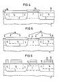
- the source / drain regions 41 of the p-channel transistors C and at the same time the p-doping of the base connection 37 of the bipolar transistor A and the gate electrode 36 are achieved by boron ion implantation with a dose and energy of 4 ⁇ 1015 cm ⁇ 2 and 40 keV generated.
- the n-channel transistor regions B and the emitter terminal 38 of the bipolar transistor A are covered with a photoresist mask.
- the distance emitter / base connection (37, 38) is defined by the spacer oxide 39.
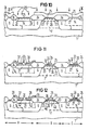
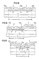
- the circuit arrangement is completed in a known manner by means of contact hole technology, metallization (single-layer or two-layer metallization) and passivation.
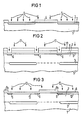
- the letters (A, B, C) shown in FIG. 12 mark the area of the bipolar transistor A and the areas of the n-channel transistor B and the p-channel transistor C.
- a p-doped substrate (1) with a specific electrical resistance of 0.02 ohm cm it is also possible to start from a p-doped substrate (1) with a specific electrical resistance of 0.02 ohm cm and to omit the implantation shown in FIG. 1 to produce the buried collector or with a starting material from 20 ohm cm to omit the implantation shown in FIG. 1 and not to apply the epitaxial layer shown in FIG. 3. Saving the buried collector simplifies the process.
Landscapes
- Engineering & Computer Science (AREA)
- Power Engineering (AREA)
- Microelectronics & Electronic Packaging (AREA)
- Physics & Mathematics (AREA)
- Condensed Matter Physics & Semiconductors (AREA)
- General Physics & Mathematics (AREA)
- Computer Hardware Design (AREA)
- Manufacturing & Machinery (AREA)
- Ceramic Engineering (AREA)
- Metal-Oxide And Bipolar Metal-Oxide Semiconductor Integrated Circuits (AREA)
- Bipolar Transistors (AREA)
- Electrodes Of Semiconductors (AREA)
Priority Applications (1)
| Application Number | Priority Date | Filing Date | Title |
|---|---|---|---|
| AT87104507T ATE94688T1 (de) | 1986-07-04 | 1987-03-26 | Integrierte bipolar- und komplementaere mostransistoren auf einem gemeinsamen substrat enthaltende schaltung und verfahren zu ihrer herstellung. |
Applications Claiming Priority (2)
| Application Number | Priority Date | Filing Date | Title |
|---|---|---|---|
| DE3622525 | 1986-07-04 | ||
| DE3622525 | 1986-07-04 |
Publications (3)
| Publication Number | Publication Date |
|---|---|
| EP0250721A2 true EP0250721A2 (fr) | 1988-01-07 |
| EP0250721A3 EP0250721A3 (en) | 1990-05-23 |
| EP0250721B1 EP0250721B1 (fr) | 1993-09-15 |
Family
ID=6304409
Family Applications (1)
| Application Number | Title | Priority Date | Filing Date |
|---|---|---|---|
| EP87104507A Expired - Lifetime EP0250721B1 (fr) | 1986-07-04 | 1987-03-26 | Circuit intégré comprenant sur un substrat commun des transistors bipolaires et des transistors MOS complémentaires et son procédé de fabrication |
Country Status (7)
| Country | Link |
|---|---|
| US (1) | US5100811A (fr) |
| EP (1) | EP0250721B1 (fr) |
| JP (1) | JP2807677B2 (fr) |
| KR (1) | KR950006984B1 (fr) |
| AT (1) | ATE94688T1 (fr) |
| CA (1) | CA1310763C (fr) |
| DE (1) | DE3787407D1 (fr) |
Cited By (9)
| Publication number | Priority date | Publication date | Assignee | Title |
|---|---|---|---|---|
| US4943536A (en) * | 1988-05-31 | 1990-07-24 | Texas Instruments, Incorporated | Transistor isolation |
| EP0403009A1 (fr) * | 1989-06-16 | 1990-12-19 | Koninklijke Philips Electronics N.V. | Méthode de fabrication d'un dispositif semi-conducteur |
| EP0427253A2 (fr) * | 1989-11-09 | 1991-05-15 | Kabushiki Kaisha Toshiba | Dispositif de circuit intégré semi-conducteur comprenant des transistors bipolaires, des TEC de type MOS et CCD |
| EP0435257A2 (fr) * | 1989-12-27 | 1991-07-03 | Oki Electric Industry Co., Ltd. | Procédé de fabrication d'un dispositif semi-conducteur biMOS à fiabilité et rapidité améliorées |
| DE4139490A1 (de) * | 1991-06-27 | 1993-01-07 | Samsung Electronics Co Ltd | Bicmos-vorrichtung und verfahren zur herstellung derselben |
| US5256582A (en) * | 1989-02-10 | 1993-10-26 | Texas Instruments Incorporated | Method of forming complementary bipolar and MOS transistor having power and logic structures on the same integrated circuit substrate |
| US5288651A (en) * | 1989-11-09 | 1994-02-22 | Kabushiki Kaisha Toshiba | Method of making semiconductor integrated circuit device including bipolar transistors, MOS FETs and CCD |
| US5336911A (en) * | 1988-05-10 | 1994-08-09 | Seiko Epson Corporation | Semiconductor device |
| WO1995023430A1 (fr) * | 1994-02-28 | 1995-08-31 | National Semiconductor Corporation | Structures bipolaires et bichos, et procedes pour leur fabrication |
Families Citing this family (12)
| Publication number | Priority date | Publication date | Assignee | Title |
|---|---|---|---|---|
| JPH01202856A (ja) * | 1988-02-09 | 1989-08-15 | Matsushita Electron Corp | 半導体集積回路の製造方法 |
| JPH025463A (ja) * | 1988-06-24 | 1990-01-10 | Hitachi Ltd | 半導体集積回路装置及びその製造方法 |
| US5318917A (en) * | 1988-11-04 | 1994-06-07 | Matsushita Electric Industrial Co., Ltd. | Method of fabricating semiconductor device |
| US5290714A (en) * | 1990-01-12 | 1994-03-01 | Hitachi, Ltd. | Method of forming semiconductor device including a CMOS structure having double-doped channel regions |
| US6249030B1 (en) * | 1992-12-07 | 2001-06-19 | Hyundai Electronics Industries Co., Ltd. | BI-CMOS integrated circuit |
| DE4308958A1 (de) * | 1993-03-21 | 1994-09-22 | Prema Paezisionselektronik Gmb | Verfahren zur Herstellung von Bipolartransistoren |
| US5652183A (en) * | 1994-01-18 | 1997-07-29 | Matsushita Electric Industrial Co., Ltd. | Method for fabricating semiconductor device containing excessive silicon in metal silicide film |
| US5439833A (en) * | 1994-03-15 | 1995-08-08 | National Semiconductor Corp. | Method of making truly complementary and self-aligned bipolar and CMOS transistor structures with minimized base and gate resistances and parasitic capacitance |
| KR0141165B1 (ko) * | 1995-03-08 | 1998-07-15 | 김광호 | 반도체장치의 트랜지스터 제조방법 |
| JPH09306924A (ja) * | 1996-03-15 | 1997-11-28 | Toshiba Corp | 半導体装置の製造方法 |
| JP3321553B2 (ja) * | 1997-10-08 | 2002-09-03 | 松下電器産業株式会社 | Bi−CMOS集積回路装置の製造方法 |
| JP6070333B2 (ja) * | 2013-03-25 | 2017-02-01 | セイコーエプソン株式会社 | 半導体装置の製造方法 |
Citations (5)
| Publication number | Priority date | Publication date | Assignee | Title |
|---|---|---|---|---|
| US4074304A (en) * | 1974-10-04 | 1978-02-14 | Nippon Electric Company, Ltd. | Semiconductor device having a miniature junction area and process for fabricating same |
| EP0010100A1 (fr) * | 1978-02-07 | 1980-04-30 | Hermes Precisa International S.A. | Dispositif de mise en place du debut de ligne dans une machine a ecrire |
| EP0101000A2 (fr) * | 1982-08-12 | 1984-02-22 | Siemens Aktiengesellschaft | Circuit semi-conducteur intégré comportant des transistors bipolaires et des transistors MOS dans un même substrat et son procédé de fabrication |
| EP0139266A2 (fr) * | 1983-10-07 | 1985-05-02 | Kabushiki Kaisha Toshiba | Dispositif semi-conducteur intégré comportant un transistor MOS et un transistor bipolaire et son procédé de fabrication |
| EP0215583A2 (fr) * | 1985-09-18 | 1987-03-25 | Advanced Micro Devices, Inc. | Dispositifs bipolaires/MOS sur des substrats à circuits intégrés |
Family Cites Families (14)
| Publication number | Priority date | Publication date | Assignee | Title |
|---|---|---|---|---|
| DE3211761A1 (de) * | 1982-03-30 | 1983-10-06 | Siemens Ag | Verfahren zum herstellen von integrierten mos-feldeffekttransistorschaltungen in siliziumgate-technologie mit silizid beschichteten diffusionsgebieten als niederohmige leiterbahnen |
| JPS5955052A (ja) * | 1982-09-24 | 1984-03-29 | Hitachi Ltd | 半導体集積回路装置の製造方法 |
| US4521952A (en) * | 1982-12-02 | 1985-06-11 | International Business Machines Corporation | Method of making integrated circuits using metal silicide contacts |
| JPS59117150A (ja) * | 1982-12-24 | 1984-07-06 | Hitachi Ltd | 半導体集積回路装置とその製造法 |
| US4554572A (en) * | 1983-06-17 | 1985-11-19 | Texas Instruments Incorporated | Self-aligned stacked CMOS |
| FR2549293B1 (fr) * | 1983-07-13 | 1986-10-10 | Silicium Semiconducteur Ssc | Transistor bipolaire haute frequence et son procede de fabrication |
| US4546536A (en) * | 1983-08-04 | 1985-10-15 | International Business Machines Corporation | Fabrication methods for high performance lateral bipolar transistors |
| JPS6058644A (ja) * | 1983-09-12 | 1985-04-04 | Toshiba Corp | 半導体装置 |
| FR2555365B1 (fr) * | 1983-11-22 | 1986-08-29 | Efcis | Procede de fabrication de circuit integre avec connexions de siliciure de tantale et circuit integre realise selon ce procede |
| JPS61110457A (ja) * | 1984-11-05 | 1986-05-28 | Nec Corp | 半導体装置 |
| JPH0666425B2 (ja) * | 1984-12-07 | 1994-08-24 | 日本電信電話株式会社 | 複合型半導体装置 |
| ATE59917T1 (de) * | 1985-09-13 | 1991-01-15 | Siemens Ag | Integrierte bipolar- und komplementaere mostransistoren auf einem gemeinsamen substrat enthaltende schaltung und verfahren zu ihrer herstellung. |
| JPH0628296B2 (ja) * | 1985-10-17 | 1994-04-13 | 日本電気株式会社 | 半導体装置の製造方法 |
| US4764482A (en) * | 1986-11-21 | 1988-08-16 | General Electric Company | Method of fabricating an integrated circuit containing bipolar and MOS transistors |
-
1987
- 1987-03-26 DE DE87104507T patent/DE3787407D1/de not_active Expired - Lifetime
- 1987-03-26 AT AT87104507T patent/ATE94688T1/de not_active IP Right Cessation
- 1987-03-26 EP EP87104507A patent/EP0250721B1/fr not_active Expired - Lifetime
- 1987-06-29 JP JP62165141A patent/JP2807677B2/ja not_active Expired - Lifetime
- 1987-07-03 CA CA000541208A patent/CA1310763C/fr not_active Expired - Fee Related
- 1987-07-04 KR KR1019870007128A patent/KR950006984B1/ko not_active IP Right Cessation
-
1990
- 1990-12-21 US US07/632,411 patent/US5100811A/en not_active Expired - Lifetime
Patent Citations (5)
| Publication number | Priority date | Publication date | Assignee | Title |
|---|---|---|---|---|
| US4074304A (en) * | 1974-10-04 | 1978-02-14 | Nippon Electric Company, Ltd. | Semiconductor device having a miniature junction area and process for fabricating same |
| EP0010100A1 (fr) * | 1978-02-07 | 1980-04-30 | Hermes Precisa International S.A. | Dispositif de mise en place du debut de ligne dans une machine a ecrire |
| EP0101000A2 (fr) * | 1982-08-12 | 1984-02-22 | Siemens Aktiengesellschaft | Circuit semi-conducteur intégré comportant des transistors bipolaires et des transistors MOS dans un même substrat et son procédé de fabrication |
| EP0139266A2 (fr) * | 1983-10-07 | 1985-05-02 | Kabushiki Kaisha Toshiba | Dispositif semi-conducteur intégré comportant un transistor MOS et un transistor bipolaire et son procédé de fabrication |
| EP0215583A2 (fr) * | 1985-09-18 | 1987-03-25 | Advanced Micro Devices, Inc. | Dispositifs bipolaires/MOS sur des substrats à circuits intégrés |
Cited By (14)
| Publication number | Priority date | Publication date | Assignee | Title |
|---|---|---|---|---|
| US5336911A (en) * | 1988-05-10 | 1994-08-09 | Seiko Epson Corporation | Semiconductor device |
| US4943536A (en) * | 1988-05-31 | 1990-07-24 | Texas Instruments, Incorporated | Transistor isolation |
| US5256582A (en) * | 1989-02-10 | 1993-10-26 | Texas Instruments Incorporated | Method of forming complementary bipolar and MOS transistor having power and logic structures on the same integrated circuit substrate |
| EP0403009A1 (fr) * | 1989-06-16 | 1990-12-19 | Koninklijke Philips Electronics N.V. | Méthode de fabrication d'un dispositif semi-conducteur |
| US4988633A (en) * | 1989-06-16 | 1991-01-29 | U.S. Philips Corporation | Method of manufacturing a semiconductor Bi-CMOS device |
| US5288651A (en) * | 1989-11-09 | 1994-02-22 | Kabushiki Kaisha Toshiba | Method of making semiconductor integrated circuit device including bipolar transistors, MOS FETs and CCD |
| EP0427253A3 (en) * | 1989-11-09 | 1991-09-11 | Kabushiki Kaisha Toshiba | Semiconductor integrated circuit device including bipolar transistors, mos fets and ccd |
| EP0427253A2 (fr) * | 1989-11-09 | 1991-05-15 | Kabushiki Kaisha Toshiba | Dispositif de circuit intégré semi-conducteur comprenant des transistors bipolaires, des TEC de type MOS et CCD |
| EP0435257A3 (en) * | 1989-12-27 | 1991-10-09 | Oki Electric Industry Co., Ltd. | Fabrication method for bimos semiconductor device with improved speed and reliability |
| EP0435257A2 (fr) * | 1989-12-27 | 1991-07-03 | Oki Electric Industry Co., Ltd. | Procédé de fabrication d'un dispositif semi-conducteur biMOS à fiabilité et rapidité améliorées |
| DE4139490A1 (de) * | 1991-06-27 | 1993-01-07 | Samsung Electronics Co Ltd | Bicmos-vorrichtung und verfahren zur herstellung derselben |
| WO1995023430A1 (fr) * | 1994-02-28 | 1995-08-31 | National Semiconductor Corporation | Structures bipolaires et bichos, et procedes pour leur fabrication |
| US5543653A (en) * | 1994-02-28 | 1996-08-06 | National Semiconductor Corporation | Bipolar and BiCMOS structures |
| US5580798A (en) * | 1994-02-28 | 1996-12-03 | National Semiconductor Corporation | Method of fabricating bipolar transistor having a guard ring |
Also Published As
| Publication number | Publication date |
|---|---|
| JPS6328060A (ja) | 1988-02-05 |
| US5100811A (en) | 1992-03-31 |
| ATE94688T1 (de) | 1993-10-15 |
| EP0250721A3 (en) | 1990-05-23 |
| JP2807677B2 (ja) | 1998-10-08 |
| KR880002245A (ko) | 1988-04-29 |
| CA1310763C (fr) | 1992-11-24 |
| EP0250721B1 (fr) | 1993-09-15 |
| DE3787407D1 (de) | 1993-10-21 |
| KR950006984B1 (ko) | 1995-06-26 |
Similar Documents
| Publication | Publication Date | Title |
|---|---|---|
| EP0219641B1 (fr) | Circuit intégré comprenant des transistors bipolaires et MOS complémentaires sur un substrat commun et méthode pour sa fabrication | |
| EP0226892B1 (fr) | Procédé pour la fabrication de transistors bipolaires et MOS-complémentaires sur un substrat commun en silicium | |
| DE3105118C2 (de) | Verfahren zur Herstellung einer integrierten Schaltung mit komplementären bipolaren Transistoren und komplementären Isolierschicht-Gate-Feldeffekttransistoren auf einem gemeinsamen Substrat | |
| EP0250721B1 (fr) | Circuit intégré comprenant sur un substrat commun des transistors bipolaires et des transistors MOS complémentaires et son procédé de fabrication | |
| EP0256315B1 (fr) | Circuit intégré contenant des transistors bipolaires et de type CMOS sur le même substrat et son procédé de fabrication | |
| EP0204979B1 (fr) | Procédé de fabrication simultanée des transistors de type MOS complémentaires et bipolaires sur le même substrat en silicium | |
| EP0227970B1 (fr) | Procédé de fabrication simultanée de transistors bipolaires auto-alignés et de transistors de type MOS complémentaires sur un substrat en silicium commun | |
| EP0244607B1 (fr) | Méthode pour fabriquer des transistors CMOS optimisés à effet de champ en technologie VLSI | |
| DE3019850C2 (fr) | ||
| US6362038B1 (en) | Low and high voltage CMOS devices and process for fabricating same | |
| CA1228178A (fr) | Technologie des circuits integres cmos | |
| EP0020998B1 (fr) | Procédé de fabrication d'un transistor bipolaire comprenant une zône d'émetteur à implantation ionique | |
| EP0248988A1 (fr) | Procédé pour fabriquer des circuits à transistors complémentaires à effet de champ du type MOS à haute intégration | |
| EP0293641B1 (fr) | Procédé de fabrication à un transistor bipolaire entièrement auto-aligné | |
| EP0232497B1 (fr) | Procédé pour la fabrication simultanée de transistors bipolaires et MOS-complémentaires sur un substrat commun en silicium | |
| EP0071665B1 (fr) | Procédé pour la fabrication d'un circuit intégré à corps solide et monolithique ayant au moins un transistor bipolaire plan | |
| EP0303050B1 (fr) | Procédé pour fabriquer des caissons séparés par des tranchées isolantes pour des circuits composés de transistors CMOS | |
| US5556796A (en) | Self-alignment technique for forming junction isolation and wells | |
| DE3022565A1 (de) | Halbleiteranordnung | |
| EP0226890A1 (fr) | Procédé de fabrication de structures de transistors bipolaires auto-alignés à résistance de base réduite | |
| EP0764982A1 (fr) | Procédé pour la fabrication d'un circuit CMOS intégré | |
| EP0197198B1 (fr) | Procédé pour fabriquer une isolation séparant les régions actives d'un circuit intégré de type CMOS à grande échelle | |
| DE3736369C2 (fr) | ||
| KR900001062B1 (ko) | 반도체 바이 씨 모오스 장치의 제조방법 | |
| EP0693775A2 (fr) | Procédé de fabrication de transistors MOS et transistors bipolaires sur une plaquette semi-conductrice |
Legal Events
| Date | Code | Title | Description |
|---|---|---|---|
| PUAI | Public reference made under article 153(3) epc to a published international application that has entered the european phase |
Free format text: ORIGINAL CODE: 0009012 |
|
| AK | Designated contracting states |
Kind code of ref document: A2 Designated state(s): AT DE FR GB IT NL SE |
|
| PUAL | Search report despatched |
Free format text: ORIGINAL CODE: 0009013 |
|
| AK | Designated contracting states |
Kind code of ref document: A3 Designated state(s): AT DE FR GB IT NL SE |
|
| 17P | Request for examination filed |
Effective date: 19900919 |
|
| 17Q | First examination report despatched |
Effective date: 19920709 |
|
| GRAA | (expected) grant |
Free format text: ORIGINAL CODE: 0009210 |
|
| AK | Designated contracting states |
Kind code of ref document: B1 Designated state(s): AT DE FR GB IT NL SE |
|
| REF | Corresponds to: |
Ref document number: 94688 Country of ref document: AT Date of ref document: 19931015 Kind code of ref document: T |
|
| REF | Corresponds to: |
Ref document number: 3787407 Country of ref document: DE Date of ref document: 19931021 |
|
| ITF | It: translation for a ep patent filed |
Owner name: STUDIO JAUMANN |
|
| GBT | Gb: translation of ep patent filed (gb section 77(6)(a)/1977) |
Effective date: 19931122 |
|
| ET | Fr: translation filed | ||
| PLBE | No opposition filed within time limit |
Free format text: ORIGINAL CODE: 0009261 |
|
| STAA | Information on the status of an ep patent application or granted ep patent |
Free format text: STATUS: NO OPPOSITION FILED WITHIN TIME LIMIT |
|
| 26N | No opposition filed | ||
| EAL | Se: european patent in force in sweden |
Ref document number: 87104507.6 |
|
| REG | Reference to a national code |
Ref country code: GB Ref legal event code: IF02 |
|
| PGFP | Annual fee paid to national office [announced via postgrant information from national office to epo] |
Ref country code: NL Payment date: 20040227 Year of fee payment: 18 |
|
| PGFP | Annual fee paid to national office [announced via postgrant information from national office to epo] |
Ref country code: SE Payment date: 20040302 Year of fee payment: 18 |
|
| PGFP | Annual fee paid to national office [announced via postgrant information from national office to epo] |
Ref country code: GB Payment date: 20040303 Year of fee payment: 18 Ref country code: AT Payment date: 20040303 Year of fee payment: 18 |
|
| PGFP | Annual fee paid to national office [announced via postgrant information from national office to epo] |
Ref country code: FR Payment date: 20040310 Year of fee payment: 18 |
|
| PG25 | Lapsed in a contracting state [announced via postgrant information from national office to epo] |
Ref country code: IT Free format text: LAPSE BECAUSE OF NON-PAYMENT OF DUE FEES;WARNING: LAPSES OF ITALIAN PATENTS WITH EFFECTIVE DATE BEFORE 2007 MAY HAVE OCCURRED AT ANY TIME BEFORE 2007. THE CORRECT EFFECTIVE DATE MAY BE DIFFERENT FROM THE ONE RECORDED. Effective date: 20050326 Ref country code: GB Free format text: LAPSE BECAUSE OF NON-PAYMENT OF DUE FEES Effective date: 20050326 Ref country code: AT Free format text: LAPSE BECAUSE OF NON-PAYMENT OF DUE FEES Effective date: 20050326 |
|
| PG25 | Lapsed in a contracting state [announced via postgrant information from national office to epo] |
Ref country code: SE Free format text: LAPSE BECAUSE OF NON-PAYMENT OF DUE FEES Effective date: 20050327 |
|
| PG25 | Lapsed in a contracting state [announced via postgrant information from national office to epo] |
Ref country code: NL Free format text: LAPSE BECAUSE OF NON-PAYMENT OF DUE FEES Effective date: 20051001 |
|
| EUG | Se: european patent has lapsed | ||
| GBPC | Gb: european patent ceased through non-payment of renewal fee |
Effective date: 20050326 |
|
| PG25 | Lapsed in a contracting state [announced via postgrant information from national office to epo] |
Ref country code: FR Free format text: LAPSE BECAUSE OF NON-PAYMENT OF DUE FEES Effective date: 20051130 |
|
| NLV4 | Nl: lapsed or anulled due to non-payment of the annual fee |
Effective date: 20051001 |
|
| REG | Reference to a national code |
Ref country code: FR Ref legal event code: ST Effective date: 20051130 |
|
| PGFP | Annual fee paid to national office [announced via postgrant information from national office to epo] |
Ref country code: DE Payment date: 20060516 Year of fee payment: 20 |