EP0246878A2 - Videosignal-Verarbeitungsschaltungen - Google Patents
Videosignal-Verarbeitungsschaltungen Download PDFInfo
- Publication number
- EP0246878A2 EP0246878A2 EP87304487A EP87304487A EP0246878A2 EP 0246878 A2 EP0246878 A2 EP 0246878A2 EP 87304487 A EP87304487 A EP 87304487A EP 87304487 A EP87304487 A EP 87304487A EP 0246878 A2 EP0246878 A2 EP 0246878A2
- Authority
- EP
- European Patent Office
- Prior art keywords
- corr
- subtracter
- signal
- luminance
- circuit
- Prior art date
- Legal status (The legal status is an assumption and is not a legal conclusion. Google has not performed a legal analysis and makes no representation as to the accuracy of the status listed.)
- Granted
Links
Images


Classifications
-
- H—ELECTRICITY
- H04—ELECTRIC COMMUNICATION TECHNIQUE
- H04N—PICTORIAL COMMUNICATION, e.g. TELEVISION
- H04N5/00—Details of television systems
- H04N5/14—Picture signal circuitry for video frequency region
- H04N5/21—Circuitry for suppressing or minimising disturbance, e.g. moiré or halo
-
- H—ELECTRICITY
- H04—ELECTRIC COMMUNICATION TECHNIQUE
- H04N—PICTORIAL COMMUNICATION, e.g. TELEVISION
- H04N9/00—Details of colour television systems
- H04N9/77—Circuits for processing the brightness signal and the chrominance signal relative to each other, e.g. adjusting the phase of the brightness signal relative to the colour signal, correcting differential gain or differential phase
- H04N9/78—Circuits for processing the brightness signal and the chrominance signal relative to each other, e.g. adjusting the phase of the brightness signal relative to the colour signal, correcting differential gain or differential phase for separating the brightness signal or the chrominance signal from the colour television signal, e.g. using comb filter
Definitions
- This invention relates to video signal processing circuits and to circuits for separating luminance and chrominance signals from video signals.
- correlation means how the signals change along a line, from line to line, or from frame to frame, respectively.
- Figure 8A illustrates a horizontal correlation Y/C separating circuit.
- a video signal applied to an input terminal 1 is supplied in common to a low pass filter 2Y and a bandpass filter 2C.
- a luminance signal Y H is supplied to an output terminal 3Y from an output of the low pass filter 2Y, and a chroma signal C H is supplied to an output terminal 3C from an output of the bandpass filter 2C.
- Figure 8B illustrates a vertical correlation Y/C separating circuit.
- An output from the 1H delay line 4 is supplied in common to the adder 5Y and the subtracter 5C.
- a luminance signal Y V from the adder 5Y is supplied to an output terminal 6Y and a chroma signal C V from the subtracter 5C is supplied to an output terminal 6C.
- Figure 8C illustrates a frame correlation Y/C separating circuit.
- a video signal applied to an input terminal 1 is supplied in common to an adder 8Y, a subtracter 8C and a frame memory 7 which constitutes a one frame delay line.
- An output of the frame memory 7 is supplied to the adder 8Y and the subtracter 8C.
- a luminance signal Y F from the adder 8Y is supplied to an output terminal 9Y and a chroma signal C F from the subtracter 8C is supplied to an output terminal 9C.
- frame memory 7 is inherently designed to process a digitised signal, it is shown to process an analog signal for the sake of simplicity. Therefore, an A/D (analog-to-digital) converter at the input side thereof and a D/A (digital-to-analog) converter at the output side thereof are not shown but are understood to be included.
- A/D analog-to-digital
- D/A digital-to-analog
- Figures 9A to 9C illustrate frequency vs. amplitude characteristics of the Y/C separating circuits shown in Figures 8A to 8C, respectively.
- a bold solid curve represents the pass band characteristic of the low pass filter 2Y and a dashed curve represents the pass band characteristic of the bandpass filter 2C.
- the low pass filter 2Y can be replaced by a subcarrier trap.
- the pass band characteristic is indicated as both bold and fine solid curves in Figure 9A.
- the vertical correlation Y/C separating circuit of Figure 8B comprises a known comb filter.
- the pass band characteristic of this comb filter relative to the luminance signal Y V is made, as shown by a solid curve in Figure 9B, to have a maximum degree of attenuation at a subcarrier frequency fsc and at respective points spaced apart therefrom by distances which are integral multiples of the horizontal frequency f H , and a minimum degree of attenuation at each of intermediate points between these points, that is at each of the points spaced apart from the subcarrier frequency fsc by a distance equal to an odd number times 1/2 of the horizontal frequency f H , that is (2n + 1) f H /2.
- the pass band characteristic thereof relative to the chroma signal C V is made, as shown by a dashed curve in Figure 9B, to have a minimum degree of attenuation at the subcarrier frequency fsc and respective points spaced apart therefrom by distances which are integral multiples of the horizontal frequency f H , and a maximum degree of attenuation at each of the points spaced apart from the subcarrier frequency fsc by a distance equal to an odd number times 1/2 of the horizontal frequency f H , that is (2n + 1) f H /2.
- the frame correlation Y/C separating circuit of Figure 8C comprises, as mentioned above, a known comb filter.
- the pass band characteristic thereof relative to the chroma signal C F is made, as shown by a dashed line in Figure 9C, to have a minimum degree of attenuation at the subcarrier frequency fsc and respective points spaced apart therefrom by distances which are integral multiples of the frame frequency f F , and a maximum degree of attenuation at respective points spaced apart from the subcarrier frequency fsc by distances equal to an odd number times 1/2 of the frame frequency f F , that is (2n + 1) f F /2.
- Figure 10B which is a partially enlarged view of Figure 10B
- the subcarrier frequency fsc and the side band wave of the vertical frequency f V accompanied thereby are located between the frequency intervals of the frame frequency f F .
- the deterioration of picture quality such as the deterioration of a frequency characteristic and the occurrence of crosstalk, occurs on the picture at right hand and left hand side edges of longitudinal stripes as shown in Figure 11A of the accompanying drawings when the levels of the luminance signal Y and the chroma signal C change abruptly in the horizontal direction.
- a video signal processing apparatus comprising a plurality of video signal correlation detecting means for detecting values of signal correlations of a video signal in a plurality of directions with respect to a picture displayed from or represented by the video signal, and intermediate value selecting means for selecting an intermediate value from among the detected values of the plurality of video signal correlations, whereby a changing video signal is processed by utilising a correlation of a proper direction.
- a changing video signal can be processed by correlation in a proper direction without detecting a moving image of the displayed picture, so that the quality of the reproduced picture can be improved.
- Preferred embodiments of this invention described in detail hereinbelow provide a video signal luminance and chrominance signal separating apparatus which can improve the quality of a reproduced picture without requiring a moving picture element detecting section.
- Figure 1 illustrates the circuit arrangement of this embodiment.
- parts corresponding to like parts of Figure 8A to 8C are designated by the same references and are not further described.
- the apparatus shown in Figure 1 comprises a horizontal correlation Y/C separating circuit H Corr, a vertical correlation Y/C separating circuit V Corr, and a frame correlation Y/C separating circuit F Corr, which are constructed as shown in Figures 8A, 8B and 8C, respectively.
- a video signal applied to an input terminal 11 is supplied in common to the Y/C separating circuits H Corr, V Corr and F Corr.
- the apparatus shown in Figure 1 comprises intermediate value selecting circuits 12Y and 12C.
- the intermediate value selecting circuit 12Y is supplied with output signals Y H , Y V and Y F of the low pass filter 2Y, the adder 5Y and the adder 8Y, respectively.
- the intermediate value selecting circuit 12C is supplied with output signals C H , C V and C F of the low pass filter 2C, the subtracter 5C and the subtracter 8C, respectively.
- Figure 2 illustrates an example of a circuit arrangement that can be employed for each of the intermediate value selecting circuits 12Y and 12C.
- the appropriate output signals of the Y/C separating circuits H Corr, V Corr and F Corr of Figure 1 are received at input terminals 21H, 21V, and 21F, respectively.
- First, second and third maximum value selecting circuits 22, 23 and 24, respectively, are connected such that an input signal from the input terminal 21H is supplied to the third and first maximum value selecting circuits 24 and 22, an input signal from the input terminal 21V is supplied to the first and second maximum value selecting circuits 22 and 23, and an input signal from the input terminal 21F is supplied to the second and third maximum value selecting circuits 23 and 24.
- Outputs A, B, C of the first to third maximum value selecting circuits 22 to 24, respectively, are all supplied to a minimum value selecting circuit 25 and an output from the minimum value selecting circuit 25 is delivered to a terminal 13.
- the amplitudes or levels of the luminance signals Y H , Y V and Y F supplied from the Y/C separating circuits H Corr, V Corr and F Corr of Figure 1 to the respective input terminals 21H, 21V and 21F of the intermediate value selecting circuit of Figure 2 satisfy the condition (amplitude or level relationship) that, for example, Y H > Y V > Y F .
- the luminance signals Y H and Y V are supplied to the first maximum value selecting circuit 22. Since the luminance signal Y H has an amplitude larger than that of the luminance signal Y V , the luminance signal Y H appears at the output A of the circuit 22.
- the second maximum value selecting circuit 23 is supplied with the luminance signals Y V and Y F . Since the luminance signal Y V has an amplitude larger than that of the luminance signal Y F , the luminance signal Y V appears at the output B of the circuit 23. Further, the third maximum value selecting circuit 24 is supplied with the luminance signals Y F and Y H . Since the luminance signal Y H has an amplitude larger than that of the luminance signal Y F , the luminance signal Y H appears at the output C of the circuit 24.
- the minimum value selecting circuit 25 is supplied with the outputs A, B and C, that is the luminance signals Y H , Y V and Y H from the maximum value selecting circuits 22 to 24, and generates the luminance signal Y V which has the smallest amplitude. Since the condition that Y H > Y V > Y F is satisfied, the intermediate value Y V is thus selected by the circuit arrangement of Figure 2.
- Table 1 below shows the outputs produced by the intermediate value selecting circuit of Figure 2 in the case in which the condition (amplitude or level relationship) relating the three luminance signals Y H , Y V and Y F is as set forth above and in other cases in which the condition is different from that set forth above.
- the intermediate value of the three luminance signals Y H , Y V and Y F is selected by the intermediate value selecting circuit.
- the intermediate value selecting circuit 12C which is also illustrated in Figure 2, is operated relative to the chroma signals C H , C V and C F in the same way as described above for the circuit 12Y.
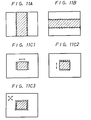
- the picture shown in Figure 11A has correlation in the vertical direction, that is the displayed image is relatively constant in the vertical direction. Conversely, the picture shown in Figure 11B has correlation in the horizontal direction. Further, correlations in the frame (time) directions appear in the still pictures shown in Figures 11C1 to 11C3, that is some part of the picture remains relatively constant from frame to frame.
- the intermediate value selecting circuit 12Y selects the luminance signal Y corresponding to the direction in which the picture has correlation.
- the other intermediate value selecting circuit 12C selects the chroma signal C corresponding to the direction in which the picture has correlation.
- the intermediate value selecting circuits 12Y or 12C can alternatively be constructed, as shown in Figure 3, by replacing the maximum value selecting circuits 22, 23 and 24 of Figure 2 with minimum value selecting circuits 26, 27 and 28 and by replacing the minimum value selecting circuit 25 of Figure 2 with a maximum value selecting circuit 29.
- the circuits 26, 27 and 28 produce outputs D, E and F, respectively.
- the intermediate value selecting circuit of Figure 3 For different amplitude or level relationships of the three luminance signals Y H , Y V and Y F , the intermediate value selecting circuit of Figure 3, for the case in which the circuit is the intermediate value relating circuit 12Y, operates in accordance with Table 2 below. For the case in which the intermediate value selecting circuit of Figure 3 is the intermediate value selecting circuit 12C, it is operated in the same way relative to the chroma signals C H , C V and C F .
- Figure 4 illustrates the circuit arrangement of this embodiment.
- parts corresponding to like parts of Figure 1 are identified by the same references and are not further described.
- the apparatus shown in Figure 4 comprises a transversal filter 31 including four unit delay lines 321, 322, 323 and 324 connected in series with one another and a weighting adding circuit 33.
- the input side of the first unit delay line 321, each of the junctions between adjacent ones of the first to fourth unit delay lines 321 to 324 and the output side of the fourth unit delay line 324 are connected to the weighting adding circuit 33.
- the transversal filter 31 is equivalent to the horizontal correlation Y/C separating circuit H Corr which is formed of the low pass filter 2Y and the bandpass filter 2C as shown in Figure 1, and is operated at a clock frequency of, for example, 4 fsc.
- Each of the unit delay lines 321 to 324 has a delay time D.
- the output from the fourth unit delay line 324 of the transversal filter 31 is supplied to a first memory 34.
- An output from the first memory 34 is supplied in common to an adder 35Y and a subtracter 35C, and an output developed at the junction between the second and third unit delay lines 322 and 323 is supplied in common to the adder 35Y and the subtracter 35C.
- the delay time of the first memory 34 is selected to be 1H-2D.
- the memory 34 and the third and fourth unit delay lines 323 and 324 of the transversal filter 31 constitute a line memory whose delay time is selected to be 1H.
- the line memory, the adder 35Y and the subtracter 35C constitute a vertical correlation Y/C separating circuit V Corr.
- the output from the first memory 34 is supplied to a second memory 37 and an output of the second memory 37 is supplied in common to a second adder 38Y and a second subtracter 38C.
- An output developed at the junction between the second and third unit delay lines 322 and 323 of the transversal filter 31 is supplied in common to the adder 38Y and the subtracter 38C.
- the second memory 37, the first memory 34 and the third and fourth unit delay lines 323 and 324 of the transversal filter 31 constitute a frame memory of which the delay time is selected to be 1F (one frame period).
- This frame memory, the second adder 38Y and the second subtracter 38C constitute a frame correlation Y/C separating circuit F Corr.
- the intermediate value selecting circuit 12Y is supplied with the outputs Y H , Y V and Y F of the transversal filter 31, the adder 35Y and the adder 38Y, respectively.
- the other intermediate value selecting circuit 12C is supplied with the outputs C H , C V and C F of the transversal filter 31, the subtracter 35C and the subtracter 38C, respectively.
- Figure 5 illustrates an example of a circuit arrangement that can be employed for each of the intermediate value selecting circuits 12Y and 12C according to this embodiment.
- Input signals applied to input terminals 21H, 21V and 21F are supplied in common to a maximum value selecting circuit 41, a minimum value selecting circuit 42 and an adder 43.
- Outputs G and H from the maximum value selecting circuit 41 and the minimum value selecting circuit 42, respectively, are supplied to a second adder 44.
- An output from the first adder 43 and an output J from the second adder 44 each are supplied to the subtracter 45 in which the output J is subtracted from the output of the adder 43.
- the circuit is operated in accordance with six amplitude or level relationships between the three luminance signals Y H , Y V and Y F , for the case in which the intermediate value selecting circuit of Figure 5 is the intermediate value selecting circuit 12Y, the circuit is operated in accordance with Table 3 below.
- the intermediate value selecting circuit is operated in the same way relative to the chroma signals C H , C V and C F for the case in which the circuit is the circuit 12C.
- the intermediate value selecting circuit shown in Figure 5 together with the horizontal correlation and frame correlation Y/C separating circuits H Corr and F Corr of Figure 4, are formed of digital circuits. This is also true for the intermediate value selecting circuits which are constructed fundamentally as shown in Figures 2 and 3.
- the embodiment of Figure 4 is operated in the same way as that of the embodiment of Figure 1, so that for a picture changing at any time, the luminance signal Y and the chroma signal C in the direction in which the picture has correlation are selected to thereby carry out optimum Y/C separation, thus improving the quality of the reproduced picture.
- a noise eliminating circuit 50 comprises horizontal, vertical and frame correlation detecting circuits 51, 52 and 53 and an intermediate value selecting circuit 54 which is supplied with outputs from the correlation detecting circuits 51 to 53.
- the correlation detecting circuits 51 to 53 correspond to the signal separating circuits described above and generate signals of the same kind as that of the aforementioned luminance signals Y H , Y V and Y F .
- the intermediate value selecting circuit 54 is constructed as shown in Figure 2, Figure 3 or Figure 5.
- the other signal to be separated may be noise.
- the noise eliminating circuit of this embodiment is operated in the same way as that of the Y/C separating circuit shown in Figure 1 or Figure 4 to thereby separate the video signal and the noise. In other words, it will be easily understood that noise can be eliminated from the video signal.
- a noise eliminating apparatus of a recursive type may be made up of the noise eliminating circuit 50 of the embodiment shown in Figure 6 and a subtracter 55.
- a first subtracter 56 may be connected to the input side of the noise eliminating circuit 50 and a second subtracter 57 may be connected to the output side of the circuit 50.
- the second subtracter 57 subtracts the output signal (which hardly contains any noise) of the noise eliminating circuit 50 from the input signal (which does contain the noise) to the noise eliminating circuit 50 to thereby separate the noise component from the video signal.
- the separated noise component which is obtained from the output of the subtracter 57, is subtracted by the subtracter 56 connected to the input side of the noise eliminating circuit 50 so as thereby to eliminate the noise contained in the input signal applied to the noise eliminating circuit 50.
- the signal-to-noise (S/N) ratio of the output signal can be improved even more.
- noise eliminating apparatus to which the present invention can be applied is not limited to the above-described embodiment: many modifications and variations could be effected by those skilled in the art.
- video signal correlations in a plurality of ways, senses or directions are detected and the intermediate value of these detected correlation values is selected, so that, without the necesssity of detecting a moving picture element, the correlation of the optimum way, sense or direction can be utilised for the picture changing at any time. According, it is possible to obtain a signal separating apparatus which can improve the quality of the reproduced picture.
Landscapes
- Engineering & Computer Science (AREA)
- Multimedia (AREA)
- Signal Processing (AREA)
- Processing Of Color Television Signals (AREA)
Applications Claiming Priority (2)
| Application Number | Priority Date | Filing Date | Title |
|---|---|---|---|
| JP115032/86 | 1986-05-20 | ||
| JP61115032A JPH07123307B2 (ja) | 1986-05-20 | 1986-05-20 | Y/c分離回路 |
Publications (3)
| Publication Number | Publication Date |
|---|---|
| EP0246878A2 true EP0246878A2 (de) | 1987-11-25 |
| EP0246878A3 EP0246878A3 (en) | 1988-12-21 |
| EP0246878B1 EP0246878B1 (de) | 1993-03-17 |
Family
ID=14652523
Family Applications (1)
| Application Number | Title | Priority Date | Filing Date |
|---|---|---|---|
| EP87304487A Expired - Lifetime EP0246878B1 (de) | 1986-05-20 | 1987-05-20 | Videosignal-Verarbeitungsschaltungen |
Country Status (7)
| Country | Link |
|---|---|
| US (2) | US4764964A (de) |
| EP (1) | EP0246878B1 (de) |
| JP (1) | JPH07123307B2 (de) |
| KR (1) | KR870011802A (de) |
| AU (1) | AU597368B2 (de) |
| CA (1) | CA1312944C (de) |
| DE (1) | DE3784769T2 (de) |
Cited By (4)
| Publication number | Priority date | Publication date | Assignee | Title |
|---|---|---|---|---|
| GB2223375A (en) * | 1988-09-30 | 1990-04-04 | Toshiba Kk | Adaptive luminance and chrominance comb filter |
| GB2243045A (en) * | 1990-01-20 | 1991-10-16 | Broadcast Television Syst | Median filter for video signals |
| EP0360380A3 (de) * | 1988-09-23 | 1992-03-18 | Sony Corporation | Komponententrennung von zusammengesetzten digitalen Videosignalen |
| CN109769108A (zh) * | 2017-11-10 | 2019-05-17 | 三星显示有限公司 | 图像信号处理电路、显示装置以及图像信号处理方法 |
Families Citing this family (11)
| Publication number | Priority date | Publication date | Assignee | Title |
|---|---|---|---|---|
| US5029001A (en) * | 1986-08-14 | 1991-07-02 | Sony Corporation | NTSC compatible TV signal transmitting system for improving vertical resolution |
| JPH0198385A (ja) * | 1987-10-09 | 1989-04-17 | Sony Corp | 相関検出方式 |
| US4930005A (en) * | 1987-12-18 | 1990-05-29 | Victor Company Of Japan, Ltd. | Circuit for removing crosstalk components in a carrier chrominance signal |
| US5166794A (en) * | 1989-03-10 | 1992-11-24 | Sony Corporation | Drop out compensating circuit with interpolation of proximate pixel signals |
| JPH03258177A (ja) * | 1990-03-08 | 1991-11-18 | Sony Corp | ノンインターレース表示装置 |
| KR940001441B1 (ko) * | 1991-07-19 | 1994-02-23 | 삼성전자 주식회사 | 운동 적응형 y/c분리기 |
| KR940004559B1 (ko) * | 1991-11-26 | 1994-05-25 | 주식회사 금성사 | 정방형 변조된 칼라 텔레비젼 수상기의 스펙트럼 분포 적응형 휘도/칼라신호 분리장치 |
| GB9214214D0 (en) * | 1992-07-03 | 1992-08-12 | Snell & Wilcox Ltd | Video signal processing |
| JP2859526B2 (ja) * | 1992-10-30 | 1999-02-17 | 三星電子株式会社 | 映像信号のノイズ除去回路 |
| KR0157480B1 (ko) * | 1994-06-18 | 1998-11-16 | 김광호 | 화상처리에서 에지방향에 적응하는 휘도신호와 색신호 분리방법 및 회로 |
| US6795580B1 (en) * | 1998-09-10 | 2004-09-21 | Tektronix, Inc. | Picture quality measurement using blockiness |
Family Cites Families (18)
| Publication number | Priority date | Publication date | Assignee | Title |
|---|---|---|---|---|
| US4050084A (en) * | 1976-07-14 | 1977-09-20 | Cbs Inc. | Comb filter for television signals having adaptive features |
| US4096516A (en) * | 1977-03-25 | 1978-06-20 | Rca Corporation | Electronic signal processing apparatus |
| US4245238A (en) * | 1979-05-11 | 1981-01-13 | Rca Corporation | Non-linear processing of video image vertical detail information |
| US4240105A (en) * | 1979-08-20 | 1980-12-16 | Yves C. Faroudja | Method and apparatus for separation of chrominance and luminance with adaptive comb filtering in a quadrature modulated color television system |
| JPS56153892A (en) * | 1980-04-28 | 1981-11-28 | Sony Corp | Comb type filter |
| JPS57111195A (en) * | 1980-12-27 | 1982-07-10 | Sony Corp | Picture filter |
| JPS57160288A (en) * | 1981-03-30 | 1982-10-02 | Sony Corp | Processing circuit for chrominance signal |
| US4365266A (en) * | 1981-04-20 | 1982-12-21 | Rca Corporation | Horizontal and vertical image detail processing of a color television signal |
| US4466016A (en) * | 1981-05-27 | 1984-08-14 | Rca Corporation | Television signal filtering system |
| US4434438A (en) * | 1981-07-10 | 1984-02-28 | Matsushita Electric Industrial Co., Ltd. | Low cost automatic equalizer |
| JPH0799804B2 (ja) * | 1981-07-13 | 1995-10-25 | ソニー株式会社 | フィルタ装置 |
| JPS5850883A (ja) * | 1981-09-21 | 1983-03-25 | Sony Corp | 分離フイルタ |
| JPS5795788A (en) * | 1981-10-14 | 1982-06-14 | Hitachi Ltd | Color television signal processor |
| JPS5939185A (ja) * | 1982-08-27 | 1984-03-03 | Sony Corp | 搬送色信号の分離回路 |
| JPS6125377A (ja) * | 1984-07-13 | 1986-02-04 | Victor Co Of Japan Ltd | ノイズリダクシヨン回路 |
| US4636840A (en) * | 1984-08-09 | 1987-01-13 | Rca Corporation | Adaptive luminance-chrominance separation apparatus |
| US4626895A (en) * | 1984-08-09 | 1986-12-02 | Rca Corporation | Sampled data video signal chrominance/luminance separation system |
| CA1243398A (en) * | 1985-01-14 | 1988-10-18 | Nec Corporation | Luminance/chrominance separating apparatus |
-
1986
- 1986-05-20 JP JP61115032A patent/JPH07123307B2/ja not_active Expired - Lifetime
-
1987
- 1987-05-19 US US07/051,911 patent/US4764964A/en not_active Expired - Lifetime
- 1987-05-19 AU AU73206/87A patent/AU597368B2/en not_active Expired
- 1987-05-19 CA CA000537341A patent/CA1312944C/en not_active Expired - Lifetime
- 1987-05-19 KR KR870004933A patent/KR870011802A/ko not_active Abandoned
- 1987-05-20 DE DE8787304487T patent/DE3784769T2/de not_active Expired - Lifetime
- 1987-05-20 EP EP87304487A patent/EP0246878B1/de not_active Expired - Lifetime
-
1988
- 1988-05-02 US US07/188,905 patent/US4839727A/en not_active Expired - Lifetime
Cited By (8)
| Publication number | Priority date | Publication date | Assignee | Title |
|---|---|---|---|---|
| EP0360380A3 (de) * | 1988-09-23 | 1992-03-18 | Sony Corporation | Komponententrennung von zusammengesetzten digitalen Videosignalen |
| GB2223375A (en) * | 1988-09-30 | 1990-04-04 | Toshiba Kk | Adaptive luminance and chrominance comb filter |
| US4980737A (en) * | 1988-09-30 | 1990-12-25 | Kabushiki Kaisha Toshiba | Luminance signal and chrominance signal separating circuit |
| GB2223375B (en) * | 1988-09-30 | 1993-01-20 | Toshiba Kk | Luminance signal and chrominance signal separating circuit |
| GB2243045A (en) * | 1990-01-20 | 1991-10-16 | Broadcast Television Syst | Median filter for video signals |
| US5148278A (en) * | 1990-01-20 | 1992-09-15 | Bts Broadcast Television Systems Gmbh | Filter circuit of the median type for video signals |
| GB2243045B (en) * | 1990-01-20 | 1994-04-27 | Broadcast Television Syst | Circuit arrangement for filtering video signals |
| CN109769108A (zh) * | 2017-11-10 | 2019-05-17 | 三星显示有限公司 | 图像信号处理电路、显示装置以及图像信号处理方法 |
Also Published As
| Publication number | Publication date |
|---|---|
| EP0246878A3 (en) | 1988-12-21 |
| JPH07123307B2 (ja) | 1995-12-25 |
| EP0246878B1 (de) | 1993-03-17 |
| US4764964A (en) | 1988-08-16 |
| DE3784769T2 (de) | 1993-09-02 |
| KR870011802A (ko) | 1987-12-26 |
| DE3784769D1 (de) | 1993-04-22 |
| US4839727A (en) | 1989-06-13 |
| AU7320687A (en) | 1987-11-26 |
| AU597368B2 (en) | 1990-05-31 |
| CA1312944C (en) | 1993-01-19 |
| JPS62271585A (ja) | 1987-11-25 |
Similar Documents
| Publication | Publication Date | Title |
|---|---|---|
| EP0246878B1 (de) | Videosignal-Verarbeitungsschaltungen | |
| US4335395A (en) | Standards conversion of color television signals | |
| US4677461A (en) | Contour detecting filter | |
| US4524382A (en) | Filter circuits | |
| US4644389A (en) | Digital television signal processing circuit | |
| GB2243045A (en) | Median filter for video signals | |
| GB2206466A (en) | Adaptive y/c separation apparatus for tv signals | |
| JPH06121335A (ja) | ルミナンス及びクロミナンス分離回路 | |
| US5025311A (en) | Video signal separating apparatus | |
| KR940001841B1 (ko) | 신호분리장치 | |
| EP0218241A2 (de) | Zweidimensionaler Kammfilter | |
| JP2596731B2 (ja) | ルミナンス/クロミナンス信号成分分離装置 | |
| JP2565182B2 (ja) | ノイズ除去回路 | |
| US5523797A (en) | Luminance signal and color signal separating circuit | |
| JPH08508862A (ja) | ビデオ信号処理 | |
| EP0153034A2 (de) | Trennfilter für Leuchtdichte-Farbsignale | |
| KR940005177B1 (ko) | 펄스패턴 억압회로를 사용하는 필터회로를 갖는 휘도/색신호 분리회로 | |
| KR920008661B1 (ko) | 영상신호 처리장치 | |
| KR940000413Y1 (ko) | 휘도 및 색신호 분리회로 | |
| KR950004652Y1 (ko) | 휘도 및 색신호분리장치 | |
| KR0141129B1 (ko) | 색신호 분리장치 | |
| JPH01206776A (ja) | 巡回型ノイズリデューサ回路 | |
| JPH05111051A (ja) | クロスカラー抑圧回路及びテレビジヨン受像機 | |
| JPS61274494A (ja) | 適応型輝度信号色信号分離フイルタ | |
| JPH0724423B2 (ja) | 動き適応型輝度信号色信号分離装置及び動き検出回路 |
Legal Events
| Date | Code | Title | Description |
|---|---|---|---|
| PUAI | Public reference made under article 153(3) epc to a published international application that has entered the european phase |
Free format text: ORIGINAL CODE: 0009012 |
|
| AK | Designated contracting states |
Kind code of ref document: A2 Designated state(s): DE FR GB NL |
|
| PUAL | Search report despatched |
Free format text: ORIGINAL CODE: 0009013 |
|
| AK | Designated contracting states |
Kind code of ref document: A3 Designated state(s): DE FR GB NL |
|
| 17P | Request for examination filed |
Effective date: 19890522 |
|
| 17Q | First examination report despatched |
Effective date: 19910423 |
|
| GRAA | (expected) grant |
Free format text: ORIGINAL CODE: 0009210 |
|
| AK | Designated contracting states |
Kind code of ref document: B1 Designated state(s): DE FR GB NL |
|
| REF | Corresponds to: |
Ref document number: 3784769 Country of ref document: DE Date of ref document: 19930422 |
|
| ET | Fr: translation filed | ||
| PLBE | No opposition filed within time limit |
Free format text: ORIGINAL CODE: 0009261 |
|
| STAA | Information on the status of an ep patent application or granted ep patent |
Free format text: STATUS: NO OPPOSITION FILED WITHIN TIME LIMIT |
|
| 26N | No opposition filed | ||
| REG | Reference to a national code |
Ref country code: GB Ref legal event code: IF02 |
|
| PGFP | Annual fee paid to national office [announced via postgrant information from national office to epo] |
Ref country code: NL Payment date: 20060503 Year of fee payment: 20 |
|
| PGFP | Annual fee paid to national office [announced via postgrant information from national office to epo] |
Ref country code: FR Payment date: 20060515 Year of fee payment: 20 |
|
| PGFP | Annual fee paid to national office [announced via postgrant information from national office to epo] |
Ref country code: GB Payment date: 20060517 Year of fee payment: 20 |
|
| PGFP | Annual fee paid to national office [announced via postgrant information from national office to epo] |
Ref country code: DE Payment date: 20060518 Year of fee payment: 20 |
|
| PG25 | Lapsed in a contracting state [announced via postgrant information from national office to epo] |
Ref country code: NL Free format text: LAPSE BECAUSE OF EXPIRATION OF PROTECTION Effective date: 20070520 |
|
| REG | Reference to a national code |
Ref country code: GB Ref legal event code: PE20 |
|
| NLV7 | Nl: ceased due to reaching the maximum lifetime of a patent |
Effective date: 20070520 |
|
| PG25 | Lapsed in a contracting state [announced via postgrant information from national office to epo] |
Ref country code: GB Free format text: LAPSE BECAUSE OF EXPIRATION OF PROTECTION Effective date: 20070519 |