EP0246530A2 - System zur Decodierung von Datensignalen - Google Patents
System zur Decodierung von Datensignalen Download PDFInfo
- Publication number
- EP0246530A2 EP0246530A2 EP87106818A EP87106818A EP0246530A2 EP 0246530 A2 EP0246530 A2 EP 0246530A2 EP 87106818 A EP87106818 A EP 87106818A EP 87106818 A EP87106818 A EP 87106818A EP 0246530 A2 EP0246530 A2 EP 0246530A2
- Authority
- EP
- European Patent Office
- Prior art keywords
- clock signal
- data signals
- frequency
- clock
- fed
- Prior art date
- Legal status (The legal status is an assumption and is not a legal conclusion. Google has not performed a legal analysis and makes no representation as to the accuracy of the status listed.)
- Granted
Links
Images
Classifications
-
- G—PHYSICS
- G08—SIGNALLING
- G08G—TRAFFIC CONTROL SYSTEMS
- G08G1/00—Traffic control systems for road vehicles
- G08G1/09—Arrangements for giving variable traffic instructions
- G08G1/091—Traffic information broadcasting
- G08G1/092—Coding or decoding of the information
-
- H—ELECTRICITY
- H03—ELECTRONIC CIRCUITRY
- H03L—AUTOMATIC CONTROL, STARTING, SYNCHRONISATION OR STABILISATION OF GENERATORS OF ELECTRONIC OSCILLATIONS OR PULSES
- H03L7/00—Automatic control of frequency or phase; Synchronisation
- H03L7/06—Automatic control of frequency or phase; Synchronisation using a reference signal applied to a frequency- or phase-locked loop
- H03L7/08—Details of the phase-locked loop
-
- H—ELECTRICITY
- H04—ELECTRIC COMMUNICATION TECHNIQUE
- H04L—TRANSMISSION OF DIGITAL INFORMATION, e.g. TELEGRAPHIC COMMUNICATION
- H04L7/00—Arrangements for synchronising receiver with transmitter
- H04L7/0079—Receiver details
- H04L7/0083—Receiver details taking measures against momentary loss of synchronisation, e.g. inhibiting the synchronisation, using idle words or using redundant clocks
-
- H—ELECTRICITY
- H04—ELECTRIC COMMUNICATION TECHNIQUE
- H04L—TRANSMISSION OF DIGITAL INFORMATION, e.g. TELEGRAPHIC COMMUNICATION
- H04L7/00—Arrangements for synchronising receiver with transmitter
- H04L7/02—Speed or phase control by the received code signals, the signals containing no special synchronisation information
- H04L7/033—Speed or phase control by the received code signals, the signals containing no special synchronisation information using the transitions of the received signal to control the phase of the synchronising-signal-generating means, e.g. using a phase-locked loop
Definitions
- the invention is based on a system according to the type of the main claim.
- RDS radio data system
- a subcarrier is modulated with digital signals.
- a subcarrier of 57 kHz is amplitude-modulated with a biphase-coded data signal using the double sideband method, the carrier being suppressed.
- the biphase coding means that no spectral lines appear in the vicinity of the carrier, so that there is compatibility with the traffic radio system.
- a synchronous demodulator is provided in the receiver, to which a regenerated subcarrier is supplied in addition to the modulated signal.
- a frequency signal is generated from this regenerated subcarrier by frequency division Corresponds to the bit frequency of the data signals and is used to decode the biphase-coded signals.
- the system according to the invention with the characterizing features of the main claim has the advantage that disturbances are recognized, the number of unusable bits can be detected and the decoding can be continued immediately when the reception starts again properly.
- the invention makes it possible to obtain information largely despite disturbances, for example to regenerate a complete, error-free telegram from several disturbed data telegrams.
- the second clock signal from a divider chain, a crystal oscillator and a frequency or phase locked loop.
- a microphone processor and corresponding programs possible.
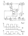
- the demodulated output signals of an FM receiver 1 are fed to a synchronous demodulator 3 via a bandpass filter 2, whose center frequency is 57 kHz.
- the output signals of the bandpass 2 are also fed to a carrier regenerator 4, which supplies a regenerated 57 kHz carrier to the synchronous demodulator 3.
- the output signals of the synchronous demodulator 3 are decoded in a decoder 6 known per se.
- a bit clock signal which is obtained from the regenerated subcarrier with the aid of a frequency divider 5, is required for decoding the output signals of the synchronous demodulator 3.
- this bit clock signal - hereinafter referred to as the first clock signal - is passed directly to the clock input of the decoder 6, the first clock signal in the system according to the invention reaches the clock input of the decoder 6 via a switch 7.
- a quartz oscillator 8 is also synchronized with the first clock signal T1. This takes place in that the first clock signal T1 is fed via a gate circuit 9 to a frequency and phase comparison circuit 10. The output voltage of the controllable quartz oscillator 8 is fed via a frequency divider 11 to a further input of the frequency and phase comparison circuit 10. Depending on the frequency and / or phase offset, a control voltage is fed to the controllable quartz oscillator via a low-pass filter 12.
- the controllable quartz oscillator 8 is tuned in frequency to the bit clock frequency of the transmitted data signal. Quartz oscillators can only be detuned by a slight change in frequency, which is not disadvantageous when using the controllable crystal oscillator 8 according to the invention, since the bit clock is generated on the transmitter side with very high accuracy. However, if there are sudden frequency or phase changes in the first clock signal T1, this is a sign that interference, in particular due to multipath reception, is present. In such a case, the output signal of the frequency divider 11 is fed to the clock input of the decoder 6 as a second clock signal T2 via the changeover switch 7.
- the first clock signal T1 and the second clock signal T2 are fed to a comparator 13. If, with the aid of this comparator, a phase deviation between the clock signals is found which exceeds a predetermined value, a signal is fed to the control input of the changeover switch 7, which switches the changeover switch 7 in brings the lower position. Furthermore, the gate circuit 9 is supplied with a signal which prevents the further supply of the first clock signal T1 to the frequency and phase comparison circuit 10. This prevents the faulty first clock signal T1 from trying to drag the controllable crystal oscillator 8.
- the output signal of the comparator 13 can be blocked by a signal supplied by a flip-flop 14.
- the flip-flop 14 is set by a pulse supplied at 15.
- a pulse is fed to input 15. It is thereby achieved that the decoder 6 is in any case operated with the first clock signal T1 in a start-up phase after switching on or after a transmitter change. Since the second clock signal T2 has a high frequency constancy and thus a high inertia, it remains in the range of the permissible deviation from the target frequency even during longer faults, but requires a longer time for synchronization after switching on or after a transmitter change.
- the first clock signal T1 in diagram a) and the second clock signal T2 in diagram b) are shown in FIG.
- Time windows are provided in the comparator 13, each of which lies in the region of the edges of the second clock signal. If the edges of the first clock signal T1 are also in these time windows, the comparator 13 emits a signal which brings the changeover switch 7 into the upper position, so that the first clock signal T1 goes to Decoder 6 is passed. This is the case with the first clock period shown in FIG. 2.
Landscapes
- Engineering & Computer Science (AREA)
- Computer Networks & Wireless Communication (AREA)
- Signal Processing (AREA)
- Multimedia (AREA)
- Physics & Mathematics (AREA)
- General Physics & Mathematics (AREA)
- Synchronisation In Digital Transmission Systems (AREA)
- Compression Or Coding Systems Of Tv Signals (AREA)
- Selective Calling Equipment (AREA)
Abstract
Description
- Die Erfindung geht aus von einem System nach der Gattung des Hauptanspruchs.
- Um zusätzlich zu Rundfunksendungen Daten übertragen zu können, ist das sogenannte Radio-Data-System (RDS) bekannt geworden, bei welchem ein Unterträger mit digitalen Signalen moduliert ist. Bei den bisher erfolgten Vorschlägen für ein derartiges System wird ein Unterträger von 57 kHz nach dem Zweiseitenbandverfahren mit einem biphase-codierten Datensignal amplitudenmoduliert, wobei der Träger unterdrückt wird. Durch die Biphase-Codierung erscheinen keine Spektrallinien in der Nähe des Trägers, so daß eine Kompatibilität zum Verkehrsfunksystem gegeben ist.
- Zur Demodulation ist im Empfänger ein Synchrondemodulator vorgesehen, welchem außer dem modulierten Signal ein regenerierter Unterträger zugeführt wird. Aus diesem regenerierten Unterträger wird durch Frequenzteilung ein Taktsignal erzeugt, welches der Bitfrequenz der Datensignale entspricht und zur Decodierung der biphase-codierten Signale herangezogen wird.
- Insbesondere bei mobilen Empfangsgeräten treten kurzzeitige Störungen auf, die ein Ausrasten des Systemtaktes bewirken können. Derartige Störungen werden insbesondere durch Mehrwegeempfang verursacht. Damit geht die Fähigkeit der Datendecodierung solange verloren, bis erneut der Anfang des Datenstroms erkannt wird.
- Das erfindungsgemäße System mit den kennzeichnenden Merkmalen des Hauptanspruchs hat demgegenüber den Vorteil, daß Störungen erkannt werden, die Anzahl der unbrauchbaren Bits erfaßt werden können und die Decodierung bei wieder einsetzendem einwandfreien Empfang sofort fortgesetzt werden kann.
- Ferner wird durch die Erfindung ermöglicht, trotz Störungen Informationen weitgehend zu gewinnen, beispielsweise aus mehreren gestörten Datentelegrammen ein vollständiges fehlerfreies Telegramm zu regenerieren.
- Durch die in den Unteransprüchen aufgeführten Maßnahmen sind vorteilhafte Weiterbildungen und Verbesserungen der im Hauptanspruch angegebenen Erfindung möglich.
- Dabei ist es in vorteilhafter Weise möglich, daß zweite Taktsignal aus einer Teilerkette, einem Quarzoszillator und einer Frequenz- oder Phasenregelschleife zu gewinnen. Es sind jedoch auch Weiterbildungen des erfindungsgemäßen Systems mit einem Mikro prozessor und entsprechenden Programmen möglich.
- Ein Ausführungsbeispiel der Erfindung ist in der Zeichnung an Hand mehrerer Figuren dargestellt und in der nachfolgenden Beschreibung näher erläutert. Es zeigt:
- Fig. 1 ein Blockschaltbild eines erfindungsgemäßen Systems und
- Fig. 2 Zeitdiagramme der bei dem System nach Fig. 1 auftretenden Taktsignale.
- Bei dem in Fig. 1 dargestellten System werden die demodulierten Ausgangssignale eines UKW-Empfängers 1 über einen Bandpaß 2, dessen Mittenfrequenz bei 57 kHz liegt, einem Synchrondemodulator 3 zugeführt. Die Ausgangssignale des Bandpasses 2 werden außerdem einem Trägerregenerator 4 zugeleitet, der einen regenerierten 57 kHz-Träger an den Synchrondemodulator 3 gibt. Die Ausgangssignale des Synchrondemodulators 3 werden in einem an sich bekannten Decoder 6 decodiert. Zur Decodierung der Ausgangssignale des Synchrondemodulators 3 ist ein Bit-Taktsignal erforderlich, welches aus dem regenerierten Unterträger mit Hilfe eines Frequenzteilers 5 gewonnen wird. Während bei dem bekannten Radio-Data-System dieses Bit-Taktsignal - im folgenden erstes Taktsignal genannt-direkt zum Takteingang des Decoders 6 geleitet wird, gelangt das erste Taktsignal bei dem erfindungsgemäßen System über einen Umschalter 7 zum Takteingang des Decoders 6.
- Mit dem ersten Taktsignal T1 wird ferner ein Quarzoszillator 8 synchronisiert. Dieses erfolgt dadurch, daß das erste Taktsignal T1 über eine Torschaltung 9 einer Frquenz- und Phasenvergleichsschaltung 10 zugeführt ist. Die Ausgangsspannung des steuerbaren Quarzoszillators 8 wird über einen Frequenzteiler 11 einem weiteren Eingang der Frequenz- und Phasenvergleichsschaltung 10 zugeführt. Je nach Frequenz- und bzw. Phasenablage wird eine Steuerspannung über einen Tiefpaß 12 dem steuerbaren Quarzoszillator zugeführt.
- Der steuerbare Quarzoszillator 8 ist bezüglich seiner Frequenz auf die Bit-Taktfrequenz des ausgesendeten Datensignals abgestimmt. Quarzoszillatoren lassen sich nur um eine geringe Frequenzänderung verstimmen, was bei der erfindungsgemäßen Anwendung des steuerbaren Quarzoszillators 8 nicht nachteilig ist, da senderseitig der Bit-Takt mit sehr hoher Genauigkeit erzeugt wird. Stellen sich jedoch plötzliche Frequenz- bzw. Phasenänderungen des ersten Taktsignals T1 ein, so ist dieses ein Zeichen dafür, daß Störungen, insbesondere durch Mehrwegeempfang, vorliegen. In einem solchen Fall wird das Ausgangssignal des Frequenzteilers 11 als zweites Taktsignal T2 über den Umschalter 7 dem Takteingang des Decoders 6 zugeführt.
- Zur Steuerung des Umschalters 7 werden das erste Taktsignal T1 und das zweite Taktsignal T2 einem Vergleicher 13 zugeführt. Wird mit Hilfe dieses Vergleichers eine Phasenabweichung zwischen den Taktsignalen festgestellt, welche ein vorgegebenes Maß überschreitet, so wird dem Steuereingang des Umschalters 7 ein Signal zugeführt, welches den Umschalter 7 in die untere Stellung bringt. Ferner wird der Torschaltung 9 ein Signal zugeführt, das die weitere Zuführung des ersten Taktsignals T1 zur Frequenz- und Phasenvergleichsschaltung 10 unterbindet. Dadurch wird verhindert, daß durch das fehlerhafte erste Taktsignal T1 versucht wird, den steuerbaren Quarzoszillator 8 nachzuziehen.
- Das Ausgangssignal des Vergleichers 13 kann durch ein von einem Flip-Flop 14 zugeführten Signal gesperrt werden. Dazu wird das Flip-Flop 14 durch einen bei 15 zugeführten Impuls gesetzt. Beim Einschalten des Gerätes und beim Wechsel des Senders wird dem Eingang 15 jeweils ein Impuls zugeführt. Dadurch wird erreicht, daß in einer Anlaufphase nach dem Einschalten bzw. nach einem Senderwechsel der Decoder 6 auf jeden Fall mit dem ersten Taktsignal T1 betrieben wird. Da das zweite Taktsignal T2 über eine hohe Frequenzkonstanz und damit über eine hohe Trägheit verfügt, bleibt es auch während längerer Störungen im Bereich der zulässigen Abweichung von der Sollfrequenz, bedarf jedoch nach dem Einschalten bzw. nach einem Senderwechsel einer längeren Zeit zum Synchronisieren.
- Zur Erläuterung der Funktion des Vergleichers 13 sind in Fig. 2 das erste Taktsignal T1 im Diagramm a) und das zweite Taktsignal T2 im Diagramm b) dargestellt. In dem Vergleicher 13 sind Zeitfenster vorgesehen, welche jeweils im Bereich der Flanken des zweiten Taktsignals liegen. Befinden sich die Flanken des ersten Taktsignals T1 ebenfalls in diesen Zeitfenstern, so wird vom Vergleicher 13 ein Signal abgegeben, welches den Umschalter 7 in die obere Stellung bringt, so daß das erste Taktsignal T1 zum Decoder 6 geleitet wird. Dieses ist bei der ersten in Fig. 2 dargestellten Taktperiode der Fall.
- Wird jedoch die Frequenz des ersten Taktsignals plötzlich höher, so gelangen die Flanken aus den Zeitfenstern. Das Ausgangssignal des Vergleichers 13 ändert seinen Pegel und bringt damit den Umschalter 7 in die untere Stellung. In Fig. 2 ist bei der zweiten Taktperiode ein Grenzfall erläutert, bei welchem die Rückflanke des zweiten Taktsignals an der Grenze des Zeitfensters liegt, während bei der dritten Taktperiode beide Flanken außerhalb der Zeitfenster liegen und somit ein gestörter Empfang vorliegt.
Claims (7)
daß ein zweites Taktsignal erzeugt wird, dessen Frequenz weitgehend unabhängig von den jeweils herrschenden Empfangsverhältnissen der Taktfrequenz der ausgesendeten Datensignale entspricht, und
daß bei Auftreten von Störungen in den empfangenen Datensignalen das zweite Taktsignal zur Decodierung der Datensignale genutzt wird.
daß das zweite Taktsignal genutzt wird, wenn die Störungen ein vorgegebenes Maß überschreiten.
daß das zweite Taktsignal genutzt wird, wenn die Phasenlage des ersten Taktsignals mehr als einen vor gegebenen Wert von der Phasenlage des zweiten Taktsignals abweicht.
daß für eine vorgegebene Zeit nach dem Einschalten und nach einem Senderwechsel nur das erste Taktsignal genutzt wird.
daß zur Erzeugung des zweiten Taktsignals ein steuerbarer Quarzoszillator (8) und eine Frequenz- und Phasenvergleichsschaltung (10) vorgesehen ist.
daß einem Decoder (6) die Datensignale und das Ausgangssignal eines Umschalters (7) zugeführt sind, daß einem ersten Eingang des Umschalters (7) das erste Taktsignal und einem zweiten Eingang das zweite Taktsignal zugeführt sind,
daß das erste und das zweite Taktsignal ferner einem Vergleicher (13) zugeführt sind, dessen Ausgang mit einem Steuereingang des Umschalters (7) und mit einem Steuereingang einer Torschaltung (9) verbunden ist, welche in der Zuführung des ersten Taktsignals zur Frequenz- und Phasenvergleichsschaltung (10) angeordnet ist.
daß an den Ausgang des Decoders eine Schaltung (14) angeschlossen ist, welche den Vergleicher (13) nach dem Einschalten und nach einem Senderwechsel vorübergehend gesperrt.
Priority Applications (1)
| Application Number | Priority Date | Filing Date | Title |
|---|---|---|---|
| AT87106818T ATE69918T1 (de) | 1986-05-16 | 1987-05-11 | System zur decodierung von datensignalen. |
Applications Claiming Priority (2)
| Application Number | Priority Date | Filing Date | Title |
|---|---|---|---|
| DE19863616590 DE3616590A1 (de) | 1986-05-16 | 1986-05-16 | System zur decodierung von datensignalen |
| DE3616590 | 1986-05-16 |
Publications (3)
| Publication Number | Publication Date |
|---|---|
| EP0246530A2 true EP0246530A2 (de) | 1987-11-25 |
| EP0246530A3 EP0246530A3 (en) | 1988-10-05 |
| EP0246530B1 EP0246530B1 (de) | 1991-11-27 |
Family
ID=6301003
Family Applications (1)
| Application Number | Title | Priority Date | Filing Date |
|---|---|---|---|
| EP87106818A Expired - Lifetime EP0246530B1 (de) | 1986-05-16 | 1987-05-11 | System zur Decodierung von Datensignalen |
Country Status (3)
| Country | Link |
|---|---|
| EP (1) | EP0246530B1 (de) |
| AT (1) | ATE69918T1 (de) |
| DE (2) | DE3616590A1 (de) |
Cited By (4)
| Publication number | Priority date | Publication date | Assignee | Title |
|---|---|---|---|---|
| FR2675972A1 (fr) * | 1991-04-25 | 1992-10-30 | Alcatel Telspace | Dispositif de recuperation de rythme. |
| WO1997044930A1 (en) * | 1996-05-23 | 1997-11-27 | Philips Electronics N.V. | Frequency generating circuit |
| EP1158706A1 (de) * | 2000-05-23 | 2001-11-28 | Sony International (Europe) GmbH | RDS Dekoder zur Reduzierung des Einflusses von Störungsspitzen unter Verwendung einer Störsperre |
| EP2267901A1 (de) * | 2009-06-19 | 2010-12-29 | Siemens Aktiengesellschaft | Verfahren und Vorrichtung zur Umsetzung eines analogen Signals |
Family Cites Families (6)
| Publication number | Priority date | Publication date | Assignee | Title |
|---|---|---|---|---|
| US3795872A (en) * | 1972-09-18 | 1974-03-05 | Bell Telephone Labor Inc | Protection scheme for clock signal recovery arrangement |
| US4369515A (en) * | 1980-10-06 | 1983-01-18 | Gte Automatic Electric Labs Inc. | Clock synchronization circuit |
| NL8201056A (nl) * | 1982-03-15 | 1983-10-03 | Philips Nv | Fm-ontvanger voor de ontvangst van fm-signalen met zenderkarakterisering. |
| DE3302700A1 (de) * | 1983-01-27 | 1984-08-02 | Siemens AG, 1000 Berlin und 8000 München | Schaltungsanordnung zum einstellen der mittenfrequenz des oszillators eines phasenregelkreises |
| DE3309270A1 (de) * | 1983-03-15 | 1984-09-20 | Siemens AG, 1000 Berlin und 8000 München | Synchronisation nachziehbarer taktoszillatoren bei der uebertragung digitaler signale |
| DE3407450A1 (de) * | 1984-02-29 | 1985-08-29 | Siemens AG, 1000 Berlin und 8000 München | Pulsregenerierschaltung |
-
1986
- 1986-05-16 DE DE19863616590 patent/DE3616590A1/de not_active Withdrawn
-
1987
- 1987-05-11 EP EP87106818A patent/EP0246530B1/de not_active Expired - Lifetime
- 1987-05-11 DE DE8787106818T patent/DE3774760D1/de not_active Expired - Fee Related
- 1987-05-11 AT AT87106818T patent/ATE69918T1/de not_active IP Right Cessation
Cited By (4)
| Publication number | Priority date | Publication date | Assignee | Title |
|---|---|---|---|---|
| FR2675972A1 (fr) * | 1991-04-25 | 1992-10-30 | Alcatel Telspace | Dispositif de recuperation de rythme. |
| WO1997044930A1 (en) * | 1996-05-23 | 1997-11-27 | Philips Electronics N.V. | Frequency generating circuit |
| EP1158706A1 (de) * | 2000-05-23 | 2001-11-28 | Sony International (Europe) GmbH | RDS Dekoder zur Reduzierung des Einflusses von Störungsspitzen unter Verwendung einer Störsperre |
| EP2267901A1 (de) * | 2009-06-19 | 2010-12-29 | Siemens Aktiengesellschaft | Verfahren und Vorrichtung zur Umsetzung eines analogen Signals |
Also Published As
| Publication number | Publication date |
|---|---|
| DE3774760D1 (de) | 1992-01-09 |
| DE3616590A1 (de) | 1987-11-19 |
| ATE69918T1 (de) | 1991-12-15 |
| EP0246530A3 (en) | 1988-10-05 |
| EP0246530B1 (de) | 1991-11-27 |
Similar Documents
| Publication | Publication Date | Title |
|---|---|---|
| EP0304799B1 (de) | Einrichtung zum Demodulieren eines Biphasesignales | |
| DE2748746C2 (de) | ||
| DE4191766C2 (de) | Frequenzsteuerschaltkreis für einen einstellbaren Empfänger-Oszillator | |
| DE68918857T2 (de) | Digitaler Empfänger mit Unter-Nyquistabtastrate. | |
| DE2907182A1 (de) | Funksignal-uebertragungssystem | |
| DE60128694T2 (de) | Datenübertragung mittels pulsbreitenmodulation | |
| DE3685616T2 (de) | Phasenverriegelte taktregenerierschaltung fuer digitale uebertragungssysteme. | |
| DE60123625T2 (de) | Datenübertragung mittels pulsbreitenmodulation | |
| EP0469622B1 (de) | Verfahren und Vorrichtung zur Demodulation eines biphasenmodulierten Signals | |
| DE4443790C1 (de) | Verfahren und Vorrichtung zur Phasensynchronisation mit einem RDS-Signal | |
| DE4444601C1 (de) | Verfahren und Vorrichtung zur empfängerseitigen RDS-Phasensynchronisation | |
| EP0291826B1 (de) | Digitaler Demodulator | |
| EP0246530A2 (de) | System zur Decodierung von Datensignalen | |
| DE3216088A1 (de) | Vorrichtung zur erkennung von signalen, die wenigstens ein erstes und ein zweites auf einer traegerwelle aufmoduliertes signal umfassen | |
| EP0256287B1 (de) | Demodulator zur Demodulation von Eingangsssignalen | |
| DE4234603C2 (de) | Demodulator- und Fehlerkorrektur-Schaltung für Radio-Daten-Signale | |
| DE19933215B4 (de) | Verfahren zum Feststellen einer RDS-Rundfunkwelle und RDS-Empfänger | |
| DE19847019A1 (de) | Demodulator für ein Multiplexsignal eines RDS-Rundfunkempfängers | |
| EP0290830B1 (de) | Demodulator zur Demodulation von Eingangssignalen | |
| DE69209890T2 (de) | MSK-Modulator | |
| DE3723343A1 (de) | Verfahren zum uebertragen eines digitalen zusatzsignals in einem ukw-fm-signal | |
| DE2051879A1 (de) | Empfanger für in einem bestimmten Signalband liegende, auf eine Tragerfre quenz aufmoduherte Impulse | |
| DE4238373C2 (de) | Schaltungsanordnung zur Regenerierung eines Hilfsträgers für die Demodulation von Radio-Daten-Signalen | |
| DE3733082A1 (de) | Fm-multiplex-rundfunkempfaenger | |
| DE4205016C2 (de) | Demodulator für Radio-Daten-Signale |
Legal Events
| Date | Code | Title | Description |
|---|---|---|---|
| PUAI | Public reference made under article 153(3) epc to a published international application that has entered the european phase |
Free format text: ORIGINAL CODE: 0009012 |
|
| AK | Designated contracting states |
Kind code of ref document: A2 Designated state(s): AT DE FR GB IT SE |
|
| PUAL | Search report despatched |
Free format text: ORIGINAL CODE: 0009013 |
|
| AK | Designated contracting states |
Kind code of ref document: A3 Designated state(s): AT DE FR GB IT SE |
|
| 17P | Request for examination filed |
Effective date: 19880825 |
|
| 17Q | First examination report despatched |
Effective date: 19901025 |
|
| GRAA | (expected) grant |
Free format text: ORIGINAL CODE: 0009210 |
|
| AK | Designated contracting states |
Kind code of ref document: B1 Designated state(s): AT DE FR GB IT SE |
|
| REF | Corresponds to: |
Ref document number: 69918 Country of ref document: AT Date of ref document: 19911215 Kind code of ref document: T |
|
| ET | Fr: translation filed | ||
| GBT | Gb: translation of ep patent filed (gb section 77(6)(a)/1977) | ||
| REF | Corresponds to: |
Ref document number: 3774760 Country of ref document: DE Date of ref document: 19920109 |
|
| ITF | It: translation for a ep patent filed | ||
| PLBE | No opposition filed within time limit |
Free format text: ORIGINAL CODE: 0009261 |
|
| STAA | Information on the status of an ep patent application or granted ep patent |
Free format text: STATUS: NO OPPOSITION FILED WITHIN TIME LIMIT |
|
| 26N | No opposition filed | ||
| EAL | Se: european patent in force in sweden |
Ref document number: 87106818.5 |
|
| PGFP | Annual fee paid to national office [announced via postgrant information from national office to epo] |
Ref country code: GB Payment date: 19960429 Year of fee payment: 10 |
|
| PGFP | Annual fee paid to national office [announced via postgrant information from national office to epo] |
Ref country code: FR Payment date: 19960517 Year of fee payment: 10 |
|
| PGFP | Annual fee paid to national office [announced via postgrant information from national office to epo] |
Ref country code: AT Payment date: 19960523 Year of fee payment: 10 |
|
| PGFP | Annual fee paid to national office [announced via postgrant information from national office to epo] |
Ref country code: SE Payment date: 19960528 Year of fee payment: 10 |
|
| PGFP | Annual fee paid to national office [announced via postgrant information from national office to epo] |
Ref country code: DE Payment date: 19960723 Year of fee payment: 10 |
|
| PG25 | Lapsed in a contracting state [announced via postgrant information from national office to epo] |
Ref country code: GB Effective date: 19970511 Ref country code: AT Effective date: 19970511 |
|
| PG25 | Lapsed in a contracting state [announced via postgrant information from national office to epo] |
Ref country code: SE Effective date: 19970512 |
|
| GBPC | Gb: european patent ceased through non-payment of renewal fee |
Effective date: 19970511 |
|
| PG25 | Lapsed in a contracting state [announced via postgrant information from national office to epo] |
Ref country code: FR Free format text: LAPSE BECAUSE OF NON-PAYMENT OF DUE FEES Effective date: 19980130 |
|
| EUG | Se: european patent has lapsed |
Ref document number: 87106818.5 |
|
| PG25 | Lapsed in a contracting state [announced via postgrant information from national office to epo] |
Ref country code: DE Free format text: LAPSE BECAUSE OF NON-PAYMENT OF DUE FEES Effective date: 19980203 |
|
| REG | Reference to a national code |
Ref country code: FR Ref legal event code: ST |
|
| PG25 | Lapsed in a contracting state [announced via postgrant information from national office to epo] |
Ref country code: IT Free format text: LAPSE BECAUSE OF NON-PAYMENT OF DUE FEES;WARNING: LAPSES OF ITALIAN PATENTS WITH EFFECTIVE DATE BEFORE 2007 MAY HAVE OCCURRED AT ANY TIME BEFORE 2007. THE CORRECT EFFECTIVE DATE MAY BE DIFFERENT FROM THE ONE RECORDED. Effective date: 20050511 |