EP0243034B1 - Programmierbarer Kontaktfleck - Google Patents
Programmierbarer Kontaktfleck Download PDFInfo
- Publication number
- EP0243034B1 EP0243034B1 EP87303030A EP87303030A EP0243034B1 EP 0243034 B1 EP0243034 B1 EP 0243034B1 EP 87303030 A EP87303030 A EP 87303030A EP 87303030 A EP87303030 A EP 87303030A EP 0243034 B1 EP0243034 B1 EP 0243034B1
- Authority
- EP
- European Patent Office
- Prior art keywords
- region
- doped
- doped region
- bonding pad
- lightly
- Prior art date
- Legal status (The legal status is an assumption and is not a legal conclusion. Google has not performed a legal analysis and makes no representation as to the accuracy of the status listed.)
- Expired - Lifetime
Links
Images


Classifications
-
- H—ELECTRICITY
- H10—SEMICONDUCTOR DEVICES; ELECTRIC SOLID-STATE DEVICES NOT OTHERWISE PROVIDED FOR
- H10W—GENERIC PACKAGES, INTERCONNECTIONS, CONNECTORS OR OTHER CONSTRUCTIONAL DETAILS OF DEVICES COVERED BY CLASS H10
- H10W20/00—Interconnections in chips, wafers or substrates
- H10W20/40—Interconnections external to wafers or substrates, e.g. back-end-of-line [BEOL] metallisations or vias connecting to gate electrodes
- H10W20/49—Adaptable interconnections, e.g. fuses or antifuses
-
- H—ELECTRICITY
- H10—SEMICONDUCTOR DEVICES; ELECTRIC SOLID-STATE DEVICES NOT OTHERWISE PROVIDED FOR
- H10B—ELECTRONIC MEMORY DEVICES
- H10B69/00—Erasable-and-programmable ROM [EPROM] devices not provided for in groups H10B41/00 - H10B63/00, e.g. ultraviolet erasable-and-programmable ROM [UVEPROM] devices
-
- H—ELECTRICITY
- H10—SEMICONDUCTOR DEVICES; ELECTRIC SOLID-STATE DEVICES NOT OTHERWISE PROVIDED FOR
- H10W—GENERIC PACKAGES, INTERCONNECTIONS, CONNECTORS OR OTHER CONSTRUCTIONAL DETAILS OF DEVICES COVERED BY CLASS H10
- H10W72/00—Interconnections or connectors in packages
- H10W72/01—Manufacture or treatment
- H10W72/012—Manufacture or treatment of bump connectors, dummy bumps or thermal bumps
-
- H—ELECTRICITY
- H10—SEMICONDUCTOR DEVICES; ELECTRIC SOLID-STATE DEVICES NOT OTHERWISE PROVIDED FOR
- H10W—GENERIC PACKAGES, INTERCONNECTIONS, CONNECTORS OR OTHER CONSTRUCTIONAL DETAILS OF DEVICES COVERED BY CLASS H10
- H10W72/00—Interconnections or connectors in packages
- H10W72/20—Bump connectors, e.g. solder bumps or copper pillars; Dummy bumps; Thermal bumps
- H10W72/251—Materials
-
- H—ELECTRICITY
- H10—SEMICONDUCTOR DEVICES; ELECTRIC SOLID-STATE DEVICES NOT OTHERWISE PROVIDED FOR
- H10W—GENERIC PACKAGES, INTERCONNECTIONS, CONNECTORS OR OTHER CONSTRUCTIONAL DETAILS OF DEVICES COVERED BY CLASS H10
- H10W72/00—Interconnections or connectors in packages
- H10W72/20—Bump connectors, e.g. solder bumps or copper pillars; Dummy bumps; Thermal bumps
- H10W72/29—Bond pads specially adapted therefor
-
- H—ELECTRICITY
- H10—SEMICONDUCTOR DEVICES; ELECTRIC SOLID-STATE DEVICES NOT OTHERWISE PROVIDED FOR
- H10W—GENERIC PACKAGES, INTERCONNECTIONS, CONNECTORS OR OTHER CONSTRUCTIONAL DETAILS OF DEVICES COVERED BY CLASS H10
- H10W72/00—Interconnections or connectors in packages
- H10W72/90—Bond pads, in general
- H10W72/931—Shapes of bond pads
- H10W72/932—Plan-view shape, i.e. in top view
-
- H—ELECTRICITY
- H10—SEMICONDUCTOR DEVICES; ELECTRIC SOLID-STATE DEVICES NOT OTHERWISE PROVIDED FOR
- H10W—GENERIC PACKAGES, INTERCONNECTIONS, CONNECTORS OR OTHER CONSTRUCTIONAL DETAILS OF DEVICES COVERED BY CLASS H10
- H10W72/00—Interconnections or connectors in packages
- H10W72/90—Bond pads, in general
- H10W72/951—Materials of bond pads
- H10W72/952—Materials of bond pads comprising metals or metalloids, e.g. PbSn, Ag or Cu
Definitions
- the present invention relates to bonding pads for semiconductor chips.
- Semiconductor chips have bonding pads which are relatively large areas of metalization providing a contact area for an assembly to solder a wire connection to one of the pins of an integrated circuit package. This wide metal area of the bonding pad is then coupled to the tiny metal connections of the integrated circuit.
- the semicustom method of designing and fabricating integrated circuits uses prefabricated semiconductor wafers which have completed circuits except for the final process step of device or component interconnection. A cost savings is realized by adapting a standard wafer, which has already been designed and manufactured, to a particular customer's needs by simply designing appropriate metal interconnections. Thus, for each customer, a metal mask is designed which connects the necessary active and passive semiconductor components to form the circuit configuration required by the customer. This method of design and fabrication allows development of a semicustom circuit in less time and at lower cost than if the entire wafer had to be independently designed for each customer.
- a bonding pad will typically be a cell area which is simply an N-doped epitaxial layer on top of a P-doped substrate.
- Inherent in this structure is a clamping diode or a capacitance.
- the clamping diode the N portion of the diode is the epitaxial region and the P portion of the diode is the substrate.
- the junction capacitor is formed at the junction of the substrate and the epitaxial region.
- JP-A-60 247 940 describes a semiconductor structure which can be connected as a PNP or an NPN transistor and which includes a metal bonding pad over a P-doped region which extends from a surface into an N-doped epitaxial region.
- the present invention is concerned with a bonding pad structure which can be connected at the metalization step to form passive or active devices in addition to forming a bonding pad.
- a programmable bonding pad structure (22; 50; 80) of a semiconductor chip which, by a suitable choice of metalisation can be contacted to form a passive or an active device in addition to forming a bonding pad, the structure comprising: a P-doped substrate (26; 68; 84); an N-doped epitaxial region (28; 56; 86) on top of said substrate; a P-doped region (34; 54; 88; 90) within the epitaxial region extending from its upper surface into said epitaxial region; a P-doped isolation region (24; 52; 82) surrounding and bordering the bonding pad structure and extending from said upper surface of the epitaxial region to said substrate; a metal bonding pad (30; 76; 98) over said P-doped region; and an N+ region
- the P-doped region allows the formation of a junction capacitance between it and the epitaxial layer.
- an oxide capacitor can be formed between the metal bonding pad and the P-doped region with an oxide layer over the P-doped region as the dielectric.
- the P-doped region can also be used as a resistance by providing metal connections to both ends.
- a vertical PNP transistor can be formed between the P-doped region, the epitaxial layer and a P-doped substrate.
- N-doped region within the P-doped region and a separate N-doped region outside of the P-doped region so that a NPN transistor can be formed.
- the outside N-doped region is preferably an N+ region coupling to a buried N+ layer. When not used as an NPN transistor, this buried N+ layer can provide a cross-under to allow routing around metal connections on the surface.
- the invention allows the possible formation in the bonding pad structure of an NPN transistor with a single or multiple emitters, a vertical PNP transistor, a junction capacitor in combination with the oxide capacitor, two matched, low value resistors and a cross-under connection.
- some of these components can be used at the same time; for example, the bonding pad can be connected to the collector of the NPN transistor and a junction capacitor can be formed between the collector and base of the transistor.
- Another possible application is the formation of a PNP vertical transistor with a bonding pad connected to its base or its emitter.
- a square shaped P-doped region is formed in the epitaxial layer. A central portion of this P-doped region is doped more heavily to be P+. A series of five N-doped regions are formed along one edge of the lightly P-doped area. Parallel to this, in the adjacent epitaxial region are formed three N+ diffused regions which couple to an N+ buried layer which extends beneath the five N-doped regions.
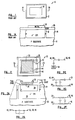
- Figure 1 shows a prior art bonding pad structure 10, which is shown in cross-section in Figure 1A.
- structure 10 is bordered with a P-doped isolation boundary 12 connecting the surface of the cell to a P-doped substrate 14 through epitaxial region 16.
- a metal layer 18 forms the bonding pad on top of an oxide layer 20.
- This structure has an inherent clamping diode between N-doped epitaxial region 16 and P-doped substrate 14, as well as a junction capacitance between these regions.
- Figures 2 and 2A show a first embodiment of the present invention.
- a bonding pad structure 22 is bordered by a P-doped isolation region 24 which connects the surface to a P-doped substrate 26 through N-doped epitaxial region 28.
- a metal bonding pad 30 is placed in an opening in oxide layer 32. Beneath metal layer 30 is a P-doped region 34.
- a thin oxide layer 36 separates bonding pad 30 from P-doped region 34.
- a pair of N+ regions 38, 40 provide connections to epitaxial region 28.
- the structure of Figure 2 can be used to form a junction capacitor between P-doped region 34 and N-doped epitaxial region 28. This can be done by providing a metal connection directly to P-doped region 34 by omitting at least a portion of thin oxide layer 36 or through openings 42, 44 in oxide layer 32. A connection to the epitaxial region 28 is provided by one or both of N+ regions 38 and 40. Alternately, an oxide capacitor is formed between P-doped region 34 and metal bonding pad 30. A connection to P-doped region 34 is provided through openings in oxide layer 32 at openings 42 and 44.
- the structure 22 can be used as a resistor by providing metal connections to openings 42 and 44 and using P-doped region 34 as a resistance. Alternately, metal connections can be provided to N+ regions 38 and 40 to provide a low resistance cross-under through epitaxial region 28.
- Figure 2B-2E Some of the circuits that can be formed from the cell of Figure 2 are shown in Figures 2B-2E.
- Figure 2B shows a junction and an oxide capacitance in parallel.
- Figure 2C shows a bonding pad coupled by an oxide capacitance to a first contact which is coupled by a junction capacitance to a second contact.
- Figure 2D shows the formation of a low resistance cross-under between N+ regions 38 and 40.
- a parasitic capacitance and diode are shown in phantom.
- Figure 2E shows the formation of two resistances, with the first resistance being the low resistance cross-under of Figure 2D and the second resistance being formed between contacts in openings 42 and 44 and bonding pad 30, with oxide layer 36 being omitted.
- pad 30 preferably only contacts P-doped region 34 at the end opposite the contacts in openings 42, 44.
- parasitic capacitance and a parasitic diode are shown in phantom.
- Figures 3-3B show a second embodiment of the present invention.
- a bonding pad structure 50 is surrounded by a P-doped isolation region 52 and has a central P-doped region 54 in epitaxial layer 56.
- a second P-doped region 58 surrounds P-doped region 54.
- An N-doped region 60 is located within P-doped region 58 along a first side of the cell. Additional N+ doped regions 62, 64 are coupled to a buried N+ layer 66.
- a PNP transistor can be formed from the structure of Figure 3 by making the connections shown in Figure 3C, and an NPN transistor can be formed by making the connections shown in Figure 3D.
- an oxide or junction capacitance can be formed in the same manner as shown for Figure 2 with a contact region 70 providing a connection to P-doped region 54 through oxide layer 72.
- a thin oxide layer 74 can be deposited on top of P-doped region 54 and a metal bonding pad 76 can be applied on top of thin oxide layer 74 to form an oxide capacitance between metal bonding pad 76 and P-doped region 54.
- metal bonding pad 76 can be used with oxide layer 74 either present or eliminated.
- Figure 4 shows a top view of a bonding pad structure 80 according to another embodiment of the present invention.
- Figure 4A is a cross-sectional view along lines 4A-4A of Figure 4.
- the structure is bordered by a P-doped isolation region 82 which couples to the P-doped substrate 84 forming an epitaxial island 86.
- a lightly P-doped region 88 is provided and has an internal more highly doped P+ region 90.
- a series of five N-doped regions 92 are located along the perimeter of one edge of P-doped region 88.
- Three N+ doped regions 94 provide connections to a buried N+ layer 96.
- a bonding pad 98 is formed over an optional thin oxide layer 100 on top of P-doped region 88.
- Figures 5A-5F show various circuits which can be formed with the structure of Figure 4.
- a junction and an oxide capacitance connected in parallel are shown.
- the oxide capacitor is formed by the common method where one plate is the aluminum metalization and the other plate is a diffused area.
- a P diffusion is used instead of using the N+ region of an emitter diffusion as in the common fabrication method. This automatically creates another capacitor, a junction capacitor, between P region 88 and N-doped epitaxial region 86.
- the two capacitors can be connected in parallel by connecting the metal bonding pad 98 to N+ regions 92.
- the junction capacitor has a value of about 0.03 x 10¹⁰ pF per square mils (0.2 pF per square mils).
- P+ region 90 can be used to form two matched low value resistors through P+ region 90 between metal bonding pad 98 (with oxide layer 100 omitted) and a pair of contact areas 102, 104.
- An NPN transistor can be formed as shown in Figure 5B with either or both of contacts 102, 104 providing the base contact, regions 92 forming the emitter and regions 94 forming the collector.
- Lightly doped P region 88 is the region coupled to by contact areas 102 and 104, providing the base of the transistor.
- Figure 5C shows one example of the metal connections that can be made on the structure of Figure 4 to form the circuit of Figure 5B.
- Metal 85 connects to contact area 104 to provide the base connection
- metal 87 connects to a region 92 to provide the emitter connection
- metal 89 connects to a region 94 to provide the collector connection.
- Figure 5D shows the connection of cell 80 of Figure 4 as a PNP transistor.
- P+ region 90 forms the emitter of the transistor
- N+ diffusion regions 94 to buried layer 96 couple to epitaxial region 86 to form the base of the transistor
- substrate 84 is the collector of the transistor.
- the substrate is usually coupled to the most negative voltage, so this transistor has its collector coupled to the most negative voltage.
- the performance of this device is much better than the usual vertical PNP because of the higher emitter concentration and the thinner base obtained with the deep P+ diffusion region 90.
- Figure 5E shows one example of the metal connections that can be made on the structure of Figure 4 to form the transistor of Figure 5D.
- Metal 91 connects to contact area 104 to provide the emitter connection
- metal 93 connects to isolation region 82, which is connected to substrate 84, to form the collector connection
- metal 95 is connected to a region 94 to provide the base connection.
- Metal bonding pad 98 can be used as a bonding pad in connection with the other functions at all times, unless the 0.6 pF capacitor between the pad and P-doped region 88 affects the circuit performance.
- the normal width of oxide layer 100 would be about 6000 x 10 ⁇ 10m (6000 angstroms), but when a higher value oxide capacitor is required, the oxide thickness can go below 2000 x 10 ⁇ 10m (2,000 angstroms).
- Figure 5F shows how NPN and PNP transistors along with junction and oxide capacitors and the bonding pad are connected together.
- the collector of a PNP transistor 106 is tied to substrate 84 which will normally be ground or the most negative voltage.
- the base 94 of PNP transistor 106 also forms the collector of an NPN transistor 108 and one side of a junction capacitor 110.
- Metal bonding pad 98 is one end of an oxide capacitor 112 with the other end being P-doped region 88, which also forms the other side of junction capacitor 110, as well as the base of NPN transistor 108 and the emitter of PNP transistor 106.
- the contact to P-doped region 88 is provided through areas 102 and 104.
- the emitter of NPN transistor 108 is contacted through regions 92.
- the present invention provides several advantages over existing semicustom designs in addition to the programmability of the bonding pad area which prevents it from being a wasted area when not used as a bonding pad. For instance, most semicustom designs do not provide integrated capacitors which are provided in the present invention. By placing the bonding pad on the periphery of the semiconductor chip, the capacitors are also on the periphery of the semiconductor chip and thus do not interfere with the routing of internal connections on the chip. By connecting the transistors of several pad structures in parallel, a high current transistor can be obtained which is ideal for an input/output interface. When not otherwise used, N+ regions 94 can provide a cross-under connection through buried layer 96.
- Standard processing methods can be used to produce the bonding pad structures according to the present invention.
- the substrate is first doped to be P.
- the N+ buried layer is then diffused and the N- epitaxial region is grown.
- Each diffusion step is performed using the standard steps of growing an oxide, depositing a photoresist coating, masking the coating, bombarding the wafer with ultraviolet light, dissolving away the noncross-linked part of the photoresist and then etching through the silicon dioxide to expose regions where diffusion will take place.
- the deep P+ diffusion to form the isolation borders for the cell is done. Thereafter, the P diffusions are done, the N diffusions are done and the oxide is etched to form the contact regions for the cell.
- Metalization is done according to the standard techniques of applying aluminium over the wafer, photomasking and etching away everywhere except where connections are desired.
Landscapes
- Semiconductor Integrated Circuits (AREA)
- Bipolar Integrated Circuits (AREA)
- Design And Manufacture Of Integrated Circuits (AREA)
- Logic Circuits (AREA)
- Semiconductor Memories (AREA)
- Wire Bonding (AREA)
Claims (10)
- Programmierbarer Kontaktfleck (22; 50; 80) auf einem Halbleiter-Chip, welcher durch geeignete Metallisierung derart zu kontaktieren ist, daß er ein passives oder ein aktives Element und zusätzlich einen Kontaktfleck bildet, der folgende Merkmale aufweist:
ein p-dotiertes Substrat (26; 68; 84);
eine n-dotierte, epitaxiale Schicht (28; 56; 86) auf dem Substrat;
eine p-dotierte Schicht (34; 54; 88; 90) innerhalb der epitaxialen Schicht, die sich von deren Oberfläche in die epitaxiale Schicht hinein erstreckt;
eine p-dotierte Isolierschicht (24; 52; 82), die den Kontaktfleck umgibt und begrenzt, und die sich von der Oberfläche der epitaxialen Schicht zu dem Substrat erstreckt;
einen über der p-dotierten Schicht angeordneten Metall-Kontaktfleck (30; 76; 98); und
eine n⁺-Schicht (38, 40; 62; 64; 94), die in der epitaxialen Schicht außerhalb der p-dotierten Schicht angeordnet ist und eine elektrische Verbindung zu der epitaxialen Schicht bildet. - Kontaktfleck nach Anspruch 1
mit einer über der p-dotierten Schicht (34; 54; 88; 90) angeordneten Oxidschicht (32; 36; 72; 74; 100) zur Bildung eines Oxidkondensators. - Kontaktfleck nach Anspruch 2
mit auf Abstand liegenden Metallkontakten, die über Löcher (42, 44) in der Oxidschicht mit der p-dotierten Schicht (34) verbunden sind zur Bildung eines Widerstandes. - Kontaktfleck nach Anspruch 1 oder 2
mit einer zweiten p-dotierten Schicht (58), die innerhalb der epitaxialen Schicht (56) angeordnet ist und die p-dotierte Schicht (54) und eine n-dotierte Schicht (60) umgibt, die innerhalb der zweiten p-dotierten Schicht (58) angeordnet ist. - Kontaktfleck nach Anspruch 4
mit einem Metallkontakt, der an die p-dotierte Schicht (54) zur Bildung des Emitters eines pnp-Transistors angeschlossen ist, einem Metallkontakt, der an die n⁺-Schicht (62, 64) zur Bildung der Basis des pnp-Transistors angeschlossen ist, und einem Kontakt, der an die zweite p-dotierte Schicht (58) zur Bildung des Kollektors des pnp-Transistors angeschlossen ist. - Kontaktfleck nach Anspruch 4
mit einem Metallkontakt, der an die n⁺-Schicht (62, 64) zur Bildung des Kollektors eines npn-Transistors angeschlossen ist; einem Metallkontakt, der an die n-dotierte Schicht (60) innerhalb der zweiten p-dotierten Schicht (58) angeschlossen ist, um den Emitter des npn-Transistors zu bilden; und einem Metallkontakt, der an die zweite p-dotierte Schicht (58) zur Bildung der Basis des npn-Transistors angeschlossen ist. - Kontaktfleck nach einem der Ansprüche 4 bis 6
mit einer überdeckten n⁺-Schicht (66), die sich in das p-dotierte Substrat (68) hinein erstreckt, wobei die genannte n⁺-Schicht (62, 64) mit der überdeckten n⁺-Schicht gekoppelt ist. - Kontaktfleck nach Anspruch 1 oder 2,
bei dem die p-dotierte Schicht aus einer schwach p-dotierten, rechteckigen Schicht (88) und einer innerhalb der schwach p-dotierten Schicht (88) angeordneten, stark p-dotierten Schicht (90) besteht; und mit
mehreren n⁺-dotierten Schichten (92) innerhalb der schwach p-dotierten Schicht (88), die an einem ersten Rand der schwach p-dotierten Schicht (88) angeordnet sind; und
einer überdeckten n⁺-Schicht (96), die sich unter dem ersten Rand der schwach p-dotierten Schicht (88) in das p-dotierte Substrat (84) hinein erstreckt;
und bei dem die n⁺-Schicht aus mehreren n⁺-Schichten (94) außerhalb der schwach p-dotierten Schicht (88) in der Nähe des ersten Randes besteht und sich in die überdeckte n⁺-Schicht (96) und die n-dotierte, epitaxiale Schicht (86) hinein erstreckt. - Kontaktfleck nach Anspruch 8
mit einem Metallkontakt (87), der an die Vielzahl von innerhalb der schwach p-dotierten Schicht (88) ausgebildeten, n⁺-dotierten Schichten (92) angeschlossen ist, um den Emitter eines npn-Transistors zu bilden; mindestens einem Metallkontakt (85, 102, 104), der an die schwach p-dotierte Schicht (88) angeschlossen ist, um die Basis des npn-Transistors zu bilden; und einem Metallkontakt (89), der an die Vielzahl von n⁺-Schichten (94) angeschlossen ist, die außerhalb der schwach p-dotierten Schicht (88) liegen, um den Kollektor des npn-Transistors zu bilden. - Kontaktfleck nach Anspruch 8
mit einem Metallkontakt (91, 102, 104), der an die schwach p-dotierte Schicht (88) angeschlossen ist, um den Emitter eines pnp-Transistors zu bilden; einem Metallkontakt (95), der an die Vielzahl von n⁺-Schichten außerhalb der schwach p-dotierten Schicht (88) angeschlossen ist, um die Basis des pnp-Transistors zu bilden; und einem Metallkontakt (93), der an die mit dem Substrat (84) verbundene, p-dotierte Isolierschicht (82) angeschlossen ist, um den Kollektor des pnp-Transistors zu bilden.
Priority Applications (1)
| Application Number | Priority Date | Filing Date | Title |
|---|---|---|---|
| AT87303030T ATE92211T1 (de) | 1986-04-17 | 1987-04-08 | Programmierbarer kontaktfleck. |
Applications Claiming Priority (2)
| Application Number | Priority Date | Filing Date | Title |
|---|---|---|---|
| US85330386A | 1986-04-17 | 1986-04-17 | |
| US853303 | 1986-04-17 |
Publications (3)
| Publication Number | Publication Date |
|---|---|
| EP0243034A2 EP0243034A2 (de) | 1987-10-28 |
| EP0243034A3 EP0243034A3 (en) | 1988-09-14 |
| EP0243034B1 true EP0243034B1 (de) | 1993-07-28 |
Family
ID=25315668
Family Applications (1)
| Application Number | Title | Priority Date | Filing Date |
|---|---|---|---|
| EP87303030A Expired - Lifetime EP0243034B1 (de) | 1986-04-17 | 1987-04-08 | Programmierbarer Kontaktfleck |
Country Status (4)
| Country | Link |
|---|---|
| EP (1) | EP0243034B1 (de) |
| JP (1) | JPS6366948A (de) |
| AT (1) | ATE92211T1 (de) |
| DE (1) | DE3786693T2 (de) |
Families Citing this family (7)
| Publication number | Priority date | Publication date | Assignee | Title |
|---|---|---|---|---|
| US4949150A (en) * | 1986-04-17 | 1990-08-14 | Exar Corporation | Programmable bonding pad with sandwiched silicon oxide and silicon nitride layers |
| JPH02220442A (ja) * | 1989-02-21 | 1990-09-03 | Fuji Electric Co Ltd | 半導体装置の保護膜補強構造 |
| US5021856A (en) * | 1989-03-15 | 1991-06-04 | Plessey Overseas Limited | Universal cell for bipolar NPN and PNP transistors and resistive elements |
| JP2566684Y2 (ja) * | 1991-09-26 | 1998-03-30 | セーレン株式会社 | 天然セリシン繊維 |
| DE19825608C1 (de) * | 1998-06-08 | 1999-09-23 | Siemens Ag | Integrierte Halbleiterschaltung mit einer Anschlußfläche, die eine fein abgestufte RC-Charakteristik aufweist |
| WO2008001248A2 (en) * | 2006-06-28 | 2008-01-03 | Nxp B.V. | Integrated circuit |
| US8058674B2 (en) * | 2009-10-07 | 2011-11-15 | Moxtek, Inc. | Alternate 4-terminal JFET geometry to reduce gate to source capacitance |
Family Cites Families (5)
| Publication number | Priority date | Publication date | Assignee | Title |
|---|---|---|---|---|
| US3573488A (en) * | 1967-09-05 | 1971-04-06 | Rca Corp | Electrical system and lsi standard cells |
| JPS607388B2 (ja) * | 1978-09-08 | 1985-02-23 | 富士通株式会社 | 半導体記憶装置 |
| US4295149A (en) * | 1978-12-29 | 1981-10-13 | International Business Machines Corporation | Master image chip organization technique or method |
| JPS60247940A (ja) * | 1984-05-23 | 1985-12-07 | Hitachi Ltd | 半導体装置およびその製造方法 |
| DE3431632A1 (de) * | 1984-08-29 | 1986-03-06 | Philips Patentverwaltung Gmbh, 2000 Hamburg | Halbleiterbauelement |
-
1987
- 1987-04-08 AT AT87303030T patent/ATE92211T1/de not_active IP Right Cessation
- 1987-04-08 DE DE87303030T patent/DE3786693T2/de not_active Expired - Fee Related
- 1987-04-08 EP EP87303030A patent/EP0243034B1/de not_active Expired - Lifetime
- 1987-04-16 JP JP62092115A patent/JPS6366948A/ja active Pending
Also Published As
| Publication number | Publication date |
|---|---|
| ATE92211T1 (de) | 1993-08-15 |
| EP0243034A3 (en) | 1988-09-14 |
| DE3786693T2 (de) | 1994-02-10 |
| EP0243034A2 (de) | 1987-10-28 |
| DE3786693D1 (de) | 1993-09-02 |
| JPS6366948A (ja) | 1988-03-25 |
Similar Documents
| Publication | Publication Date | Title |
|---|---|---|
| US5773899A (en) | Bonding pad for a semiconductor chip | |
| US5229307A (en) | Method of making extended silicide and external contact | |
| US3808475A (en) | Lsi chip construction and method | |
| US5807783A (en) | Surface mount die by handle replacement | |
| US5449946A (en) | Semiconductor device provided with isolation region | |
| EP0323856A2 (de) | Substratsstruktur für zusammengesetztes Halbleiterbauelement | |
| EP0190070B1 (de) | Halbleiterstruktur | |
| KR920003438B1 (ko) | 샌드위치된 산화 실리콘층과 질화 실리콘층을 갖는 프로그램 가능 접속패드 | |
| US7132347B2 (en) | Semiconductor device with trench structure and method for manufacturing the same | |
| US4949150A (en) | Programmable bonding pad with sandwiched silicon oxide and silicon nitride layers | |
| EP0243034B1 (de) | Programmierbarer Kontaktfleck | |
| US4631570A (en) | Integrated circuit having buried oxide isolation and low resistivity substrate for power supply interconnection | |
| US5068702A (en) | Programmable transistor | |
| US4482914A (en) | Contact structure of semiconductor device | |
| US5424575A (en) | Semiconductor device for SOI structure having lead conductor suitable for fine patterning | |
| US4672415A (en) | Power thyristor on a substrate | |
| US6445071B1 (en) | Semiconductor device having an improved multi-layer interconnection structure and manufacturing method thereof | |
| EP0450320A1 (de) | Integriertes Halbleiter-Schaltkreiselement zur Hochfrequenzsignalverarbeitung | |
| US3659156A (en) | Semiconductor device | |
| EP0240273A2 (de) | Programmierbare Transistoren | |
| TWI857265B (zh) | 半導體裝置及其製程 | |
| US5046160A (en) | Masterslice integrated circuit device having an improved wiring structure | |
| JP2664911B2 (ja) | 半導体装置 | |
| JPH02135770A (ja) | 半導体集積回路 | |
| JPS6134971A (ja) | 半導体装置 |
Legal Events
| Date | Code | Title | Description |
|---|---|---|---|
| PUAI | Public reference made under article 153(3) epc to a published international application that has entered the european phase |
Free format text: ORIGINAL CODE: 0009012 |
|
| AK | Designated contracting states |
Kind code of ref document: A2 Designated state(s): AT DE FR GB IT NL |
|
| PUAL | Search report despatched |
Free format text: ORIGINAL CODE: 0009013 |
|
| AK | Designated contracting states |
Kind code of ref document: A3 Designated state(s): AT DE FR GB IT NL |
|
| 17P | Request for examination filed |
Effective date: 19890116 |
|
| 17Q | First examination report despatched |
Effective date: 19901112 |
|
| GRAA | (expected) grant |
Free format text: ORIGINAL CODE: 0009210 |
|
| AK | Designated contracting states |
Kind code of ref document: B1 Designated state(s): AT DE FR GB IT NL |
|
| REF | Corresponds to: |
Ref document number: 92211 Country of ref document: AT Date of ref document: 19930815 Kind code of ref document: T |
|
| REF | Corresponds to: |
Ref document number: 3786693 Country of ref document: DE Date of ref document: 19930902 |
|
| ITF | It: translation for a ep patent filed | ||
| ET | Fr: translation filed | ||
| PLBE | No opposition filed within time limit |
Free format text: ORIGINAL CODE: 0009261 |
|
| STAA | Information on the status of an ep patent application or granted ep patent |
Free format text: STATUS: NO OPPOSITION FILED WITHIN TIME LIMIT |
|
| 26N | No opposition filed | ||
| PGFP | Annual fee paid to national office [announced via postgrant information from national office to epo] |
Ref country code: AT Payment date: 19950314 Year of fee payment: 9 |
|
| PGFP | Annual fee paid to national office [announced via postgrant information from national office to epo] |
Ref country code: GB Payment date: 19950327 Year of fee payment: 9 |
|
| PGFP | Annual fee paid to national office [announced via postgrant information from national office to epo] |
Ref country code: NL Payment date: 19950430 Year of fee payment: 9 |
|
| PG25 | Lapsed in a contracting state [announced via postgrant information from national office to epo] |
Ref country code: GB Effective date: 19960408 Ref country code: AT Effective date: 19960408 |
|
| PG25 | Lapsed in a contracting state [announced via postgrant information from national office to epo] |
Ref country code: NL Effective date: 19961101 |
|
| GBPC | Gb: european patent ceased through non-payment of renewal fee |
Effective date: 19960408 |
|
| NLV4 | Nl: lapsed or anulled due to non-payment of the annual fee |
Effective date: 19961101 |
|
| PGFP | Annual fee paid to national office [announced via postgrant information from national office to epo] |
Ref country code: FR Payment date: 19980319 Year of fee payment: 12 |
|
| PGFP | Annual fee paid to national office [announced via postgrant information from national office to epo] |
Ref country code: DE Payment date: 19980326 Year of fee payment: 12 |
|
| PG25 | Lapsed in a contracting state [announced via postgrant information from national office to epo] |
Ref country code: FR Free format text: LAPSE BECAUSE OF NON-PAYMENT OF DUE FEES Effective date: 19991231 |
|
| REG | Reference to a national code |
Ref country code: FR Ref legal event code: ST |
|
| PG25 | Lapsed in a contracting state [announced via postgrant information from national office to epo] |
Ref country code: DE Free format text: LAPSE BECAUSE OF NON-PAYMENT OF DUE FEES Effective date: 20000201 |
|
| PG25 | Lapsed in a contracting state [announced via postgrant information from national office to epo] |
Ref country code: IT Free format text: LAPSE BECAUSE OF NON-PAYMENT OF DUE FEES;WARNING: LAPSES OF ITALIAN PATENTS WITH EFFECTIVE DATE BEFORE 2007 MAY HAVE OCCURRED AT ANY TIME BEFORE 2007. THE CORRECT EFFECTIVE DATE MAY BE DIFFERENT FROM THE ONE RECORDED. Effective date: 20050408 |