EP0240953A2 - Halbleiterbauelement aus Schichtverbund - Google Patents
Halbleiterbauelement aus Schichtverbund Download PDFInfo
- Publication number
- EP0240953A2 EP0240953A2 EP87104995A EP87104995A EP0240953A2 EP 0240953 A2 EP0240953 A2 EP 0240953A2 EP 87104995 A EP87104995 A EP 87104995A EP 87104995 A EP87104995 A EP 87104995A EP 0240953 A2 EP0240953 A2 EP 0240953A2
- Authority
- EP
- European Patent Office
- Prior art keywords
- layer
- compound semiconductor
- gaas
- inas
- semiconductor device
- Prior art date
- Legal status (The legal status is an assumption and is not a legal conclusion. Google has not performed a legal analysis and makes no representation as to the accuracy of the status listed.)
- Withdrawn
Links
Images

Classifications
-
- H—ELECTRICITY
- H10—SEMICONDUCTOR DEVICES; ELECTRIC SOLID-STATE DEVICES NOT OTHERWISE PROVIDED FOR
- H10D—INORGANIC ELECTRIC SEMICONDUCTOR DEVICES
- H10D30/00—Field-effect transistors [FET]
- H10D30/40—FETs having zero-dimensional [0D], one-dimensional [1D] or two-dimensional [2D] charge carrier gas channels
- H10D30/47—FETs having zero-dimensional [0D], one-dimensional [1D] or two-dimensional [2D] charge carrier gas channels having two-dimensional [2D] charge carrier gas channels, e.g. nanoribbon FETs or high electron mobility transistors [HEMT]
- H10D30/471—High electron mobility transistors [HEMT] or high hole mobility transistors [HHMT]
- H10D30/473—High electron mobility transistors [HEMT] or high hole mobility transistors [HHMT] having confinement of carriers by multiple heterojunctions, e.g. quantum well HEMT
- H10D30/4732—High electron mobility transistors [HEMT] or high hole mobility transistors [HHMT] having confinement of carriers by multiple heterojunctions, e.g. quantum well HEMT using Group III-V semiconductor material
-
- H—ELECTRICITY
- H10—SEMICONDUCTOR DEVICES; ELECTRIC SOLID-STATE DEVICES NOT OTHERWISE PROVIDED FOR
- H10D—INORGANIC ELECTRIC SEMICONDUCTOR DEVICES
- H10D62/00—Semiconductor bodies, or regions thereof, of devices having potential barriers
- H10D62/80—Semiconductor bodies, or regions thereof, of devices having potential barriers characterised by the materials
- H10D62/81—Semiconductor bodies, or regions thereof, of devices having potential barriers characterised by the materials of structures exhibiting quantum-confinement effects, e.g. single quantum wells; of structures having periodic or quasi-periodic potential variation
- H10D62/815—Semiconductor bodies, or regions thereof, of devices having potential barriers characterised by the materials of structures exhibiting quantum-confinement effects, e.g. single quantum wells; of structures having periodic or quasi-periodic potential variation of structures having periodic or quasi-periodic potential variation, e.g. superlattices or multiple quantum wells [MQW]
- H10D62/8161—Semiconductor bodies, or regions thereof, of devices having potential barriers characterised by the materials of structures exhibiting quantum-confinement effects, e.g. single quantum wells; of structures having periodic or quasi-periodic potential variation of structures having periodic or quasi-periodic potential variation, e.g. superlattices or multiple quantum wells [MQW] potential variation due to variations in composition or crystallinity, e.g. heterojunction superlattices
- H10D62/8162—Semiconductor bodies, or regions thereof, of devices having potential barriers characterised by the materials of structures exhibiting quantum-confinement effects, e.g. single quantum wells; of structures having periodic or quasi-periodic potential variation of structures having periodic or quasi-periodic potential variation, e.g. superlattices or multiple quantum wells [MQW] potential variation due to variations in composition or crystallinity, e.g. heterojunction superlattices having quantum effects only in the vertical direction, i.e. layered structures having quantum effects solely resulting from vertical potential variation
- H10D62/8164—Semiconductor bodies, or regions thereof, of devices having potential barriers characterised by the materials of structures exhibiting quantum-confinement effects, e.g. single quantum wells; of structures having periodic or quasi-periodic potential variation of structures having periodic or quasi-periodic potential variation, e.g. superlattices or multiple quantum wells [MQW] potential variation due to variations in composition or crystallinity, e.g. heterojunction superlattices having quantum effects only in the vertical direction, i.e. layered structures having quantum effects solely resulting from vertical potential variation comprising only semiconductor materials
Definitions
- This invention relates to a compound semiconductor device, and more particularly to a novel compound semiconductor device increased in the electron mobility, by alternately laminating In x Ga 1-x As layer (0.7 ⁇ x 5 1.0) and In Ga 1-y As layer (0 ⁇ y ⁇ 0.3) which differ significantly in the lattice constant, and doping n-type impurities only into the In y Ga 1-y As layer (0 5 y ⁇ 0.3), so as to realize a structure different from the existing lattice-matched alternate laminating structure of GaAs and GaAlAs or GaAs and AlAs (in both pairs, the lattice mismatching is about less than 0.3%; the lattice mismatching (%) is defined as ⁇ [(lattice constant of GaAlAs or AlAs) - (lattice constant of GaAs)] x 100]/(lattice constant of GaAs)].
- the epitaxial growth method is generally employed owing to the thin and uniform growth of layer and ease of control of constituent element composition ratio.
- the molecular beam epitaxial (MBE) growth method is known as one of the particularly noticed techniques recently.
- MBE molecular beam epitaxial
- the crystal growth speed can be controlled on a single atomic plane level (see J . P. van der Ziel et al., J. Appl. Phys., 48 (1977), p. 3018), and, furthermore, when combined with the reflective electron diffraction method, the composition of one atomic plane can be accurately controlled (see J. H. Neave et al., Appl. Phys. A 31, 1, 1983).
- HEMT high electron mobility transistor
- microwave elements using conventional compound semiconductors are disclosed, for example, in the Japanese Unexamined Patent Publication Nos. 4085/1984 and 147169/1983.
- a GaAs layer 12 functioning as a buffer layer is formed on a semi-insulating GaAs substrate 11, and an undoped GaAs layer 13 serving as a channel layer is formed thereon.
- an electron supply layer 14 having a high impurity concentration such as n-Ga x Al 1-x As
- a layer 15 made of a semiconductor containing p-type impurities at high concentration and possessing a large electrophilic ability while a gate electrode 16 is disposed on this layer 15.
- the surface region 17 of the electron supply layer 14 at both sides of the layer 15 is alloyed, and a source electrode 18 and a drain electrode 19 are formed thereon.
- Fig. 3 makes use of the electron storage layer at the single hetero interface of GaAs layer and GaAlAs layer, whereas examples of making use of plural hetero interface of GaAs layer and GaAlAs layer by forming a multi-layer structure by alternately laminating GaAs layer and GaAlAs layer are described in details by R. Dingle et al. in Appl. Phys. Lett., 33, 665 (1978), and by T. J. Drummond et al., in J. Appl. Phys., 53 (2), 1023 (1982), and others.
- GaAs channel layer and Ga x Al 1-x As or AlAs electron supply layer are formed on GaAs substrate, or In 0.53 Ga 0.47 As channel layer and In O . 52 AI O . 48 As electron supply layer are formed on InP substrate.
- the difference of energy gap on the hetero interface between the channel layer and the electron supply layer is only about 0.7 eV at most (when using GaAs as the channel layer and AlAs as the electron supply layer).
- the composition rate y in Ga y Al 1-y As is usually selected somewhere between 0.7 and 0.8.
- the energy gap difference on the hetero interface between the channel layer (GaAs layer) and the electron supply layer (GaAl- As layer) is only about 0.2 eV.
- AlAs x Sb 1-x contains two elements, Al and Sb, which are easily oxidized, it is difficult to obtain a layer of high purity (the purity before Si doping), and handling of fine processing after growth is difficult.
- AlAs x Sb 1-x layer but also three-element mixed crystal or four-element mixed crystal such as In 0,53 Ga 0.47 As or In 0,52 A 0.48 As is generally complicated in composition control for lattice matching, and the growth technology is extremely difficult, which may bring about new problems, such as poor reproducibility and difficulty in unifying the composition distribution within wafer plane.
- GaAs-AlAs (or Ga x Al 1-x As) is studied predominantly.
- Ga x Al 1-x As As clear from Fig. 4, since the lattice mismatching between GaAs and AlAs is very small, about 0.3%, the lattice matching condition with GaAs is satisfied regardless of the composition rate x of Ga x Al 1-x As, so that strict composition control is not required as compared with such combinations as In Gal As-In x Al 1-x As etc. Hence, growth technology is not so difficult.
- the energy gap difference is limited up to about 0.2 eV.
- smallness of energy gap difference that is, smallness of degree of energy discontinuity on the hetero interface induces to decrease the effect of electron confinement in the two-dimensional electron gas layer mentioned above, to lower the degree of formation of two-dimensional electron gas at room temperature, and to lower the electron mobility on the hetero interface.
- This invention is contrived in the light of the above problems, it is hence a primary object of this invention to present a compound semiconductor device capable of forming a hetero interface having a high electron mobility even at room temperature, by restricting the decrease of effect of electron confinement into two-dimensional gas layer at room temperature.
- the compound semiconductor device of this invention possesses a channel layer increased in the probability of existence of electrons at the side of In x Ga 1-x As compound semiconductor layer (0.7 ⁇ x ⁇ 1.0), by alternately laminating In x Ga 1-x As compound semiconductor layer (0.7 ⁇ x ⁇ 1.0) with thickness of 16 atomic planes or less and In y Ga 1-y As compound semiconductor layer (0 ⁇ y ⁇ 0.3) with thickness of 14 atomic planes or less, so that the thickness of the former is greater than that of the latter, and by doping n-type impurities only to the In y Ga 1-y As layer (0 S y - 0.3) side.
- the ratio of In to Ga, In/Ga should be preferably 1.1 or more.
- this channel layer may be formed on a semi-insulating GaAs substrate or semi-insulating InP substrate as the substrate of a compound semiconductor device, and the lower most layer of the channel layer may be an In Ga 1-y As compound semiconductor layer (0 ⁇ y S 0.3) with thickness of 14 atomic planes or less.
- the compound semiconductor device without admitting the lattice mismatching transition, not only the In x Ga 1-x As compound semiconductor layer (0.7 ⁇ x 6 1.0) and In Ga 1-y As compound semiconductor layer (0 S y ⁇ 0.3) can be alternately laminated, but also the energy gap is increased, so that a high electron mobility can be achieved.
- a compound semiconductor thin films differing in lattice constant can be grown epitaxially without admitting defects, such as transition, etc. within the thin films (see M. J. Ludowise et al., A. P. L. 42 (1983), 487, or G. C. Osbourn et al., A. P. L., 41 (1982), 172).
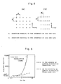
- the lattice constant of InAs (approx. 6.05 A) is 0 greater than that of GaAs (approx. 5.65 A)
- the atomic configuration in the I nAs crystal has a structure as shown in Fig. 5 (b) because of elastic distortion, different from the original structure free from elastic distortion as shown in Fig. 5 (a).
- the probability of existence of electrons at the InAs layer side where crystal lattice is elastically deformed tetragonally is increased on the interface of InAs-GaAs.
- the difference of energy gap between GaAs and InAs is about 1.0 eV, which is greater than the energy gap difference between GaAs and AlAs. Therefore, the decrease of effect of electron confinement into the InAs layer is notably restrained as compared with the case of combination of GaAs-AlAs.
- the probability of existence of electrons can be increased.
- the energy gap difference of InAs and GaAs is greater than that of conventional GaAs and Ga x Al 1-x As, and even at room temperature, the probability of existence of electrons in the InAs layer is greater, so that the electron mobility is increased.
- the degree of lattice scattering due to thermal vibration of atoms may be controlled smaller than in the case of Fig. 5 (a) free from elastic distortion.
- the lattice scattering which is a scattering mechanism of electrons at room temperature may be also decreased.
- the electron mobility at room temperature in GaAs crystal and InAs crystal is greater in the InAs crystal, but as the InAs crystal is tetragonally deformed due to elastic distortion as mentioned above, the mobility at room temperature of electrons advancing in the X-direction in the tetragonally deformed InAs layer is greater as compared with the original InAs crystal free from tetragonal deformation. Therefore, as compared with the conventional compound semiconductor device, a faster operating compound semiconductor device can be realized. Meanwhile, such compound semiconductor device fabricated by alternately laminating thin film layers of InAs layer and GaAs layer, and doping n-type impurities only at GaAs layer side to form a channel layer has not been present so far.
- the difference of energy gap between In x Ga 1-x As layer (0. 7 S x S 1.0) and In y Ga 1-y As (0 S y ⁇ 0.3) is similar to or greater than the energy gap difference of In 0.53 Ga 0.47 As and In 0.52 Al 0.48 As.
- this inventor discovered that the electric characteristics could be improved by setting the ratio of In to Ga in the entire channel structure composed of the multi-layer periodic structure stated above, In/Ga, at 1.1 or more. This fact has been found on the basis that, when the electric characteristics were measured by fabricating a compound semiconductor device by variously changing the ratio of In to Ga in the entire channel layer above, the electric characteristics were better when the ratio In/Ga was 1.1 or more than when it was less than 1.1.
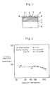
- Fig. 1 is a sectional view illustrating the FET as an embodiment of a compound semiconductor device by this invention.
- the FET shown in Fig. 1 possesses a channel layer in a structure in which InAs layer (3 atomic planes thick) 1 and GaAs layer (1 atomic plane thick) '2, which are formed by MBE growth method, are alternately laminated on a semi-insulating InP substrate 8.
- 1 atomic plane thickness means the distance between lattice planes where group III atoms (Ga, In, etc.) are present.
- Si is doped as an n-type impurity.
- the number of layers laminated is 150 for both InAs layer and GaAs layer, and the thickness of channel layer is about 0 .18 um.
- the mean carrier density of the entire channel layer was selected somewhere between approx. 1 x 10 17 c m7 3 to 5 x 1017 cm-3.
- Fig. 2 shows the results of measurement relating to temperature dependency of electron mobility of this channel layer (sample S3).
- sample Al the electron mobility of an In Ga 1-x As mixed crystal (x 1 0.8) of which In composition is greater than sample S3 was also measured (sample Al).
- sample Al the electron mobility of sample S3 is greater than that of sample Al.
- the In composition is higher, the electron mobility in high temperature region should be greater, but the In composition of sample S3 is lower than that of sample Al.
- the degree of scattering due to thermal vibration of atoms is smaller by periodic structure as in sample S3 as the scattering factor on electrons predominant in the high temperature region is due to thermal vibration of atoms.
- the mobility of sample S3 may be greater than the electron mobility estimated from the mean In composition of channel layer.
- a source electrode 3 and drain electrode 4 are disposed so as to form an ohmic junction against the channel layer, by using AuGeNi alloy.
- AuGeNi alloy After evaporating AuGeNi alloy, the alloy was heated at 400°C. At this time, atoms of Au and Ge diffused within the channel layer, and in this diffused region 6, the periodic structure of InAs and GaAs was broken and a mixed crystal was formed, so that an ohmic junction could be formed easily.
- Such phenomenon of mixed crystal due to breakage of periodic structure composed of thin film layers by partial selective diffusion was described in details by N. Holonyak et al., A. P.
- a gate electrode 5 is disposed on the outermost surface of the sample.
- the gate electrode forming method is not limited to this, and any known method may be employed.
- the InAs layer has its crystal structure elastically deformed tetragonally as shown in Fig. 5 (b), and a greater energy discontinuity is present on the interface of InAs and GaAs, than on the conventional GaAs-Ga x A 1-x As system, and also the probability of existence of electrons in the InAs layer can be heightened than that in the GaAs layer because only the GaAs layer is doped with Si.
- the degree of depletion of channel layer of about 0.18 ⁇ m thickness under the gate electrode can be controlled, and the characteristics in high electric field application or at room temperature are superior in this FET, as compared with the FET using the conventional GaAs-Ga x Al 1-x As system.
- the lowermost layer of the channel layer is the InAs layer 1, but when the channel layer is formed by using GaAs layer as the lowermost layer, the flatness of the outermost surface of the channel layer is improved, and a gate electrode with excellent Schottky characteristics may be obtained.
Landscapes
- Junction Field-Effect Transistors (AREA)
- Recrystallisation Techniques (AREA)
Applications Claiming Priority (2)
| Application Number | Priority Date | Filing Date | Title |
|---|---|---|---|
| JP78499/86 | 1986-04-05 | ||
| JP7849986 | 1986-04-05 |
Publications (2)
| Publication Number | Publication Date |
|---|---|
| EP0240953A2 true EP0240953A2 (de) | 1987-10-14 |
| EP0240953A3 EP0240953A3 (de) | 1990-05-02 |
Family
ID=13663654
Family Applications (1)
| Application Number | Title | Priority Date | Filing Date |
|---|---|---|---|
| EP87104995A Withdrawn EP0240953A3 (de) | 1986-04-05 | 1987-04-03 | Halbleiterbauelement aus Schichtverbund |
Country Status (5)
| Country | Link |
|---|---|
| US (1) | US4823171A (de) |
| EP (1) | EP0240953A3 (de) |
| JP (1) | JP2557373B2 (de) |
| AU (1) | AU593086B2 (de) |
| CA (1) | CA1262293A (de) |
Families Citing this family (5)
| Publication number | Priority date | Publication date | Assignee | Title |
|---|---|---|---|---|
| JPS62256478A (ja) * | 1986-04-30 | 1987-11-09 | Sumitomo Electric Ind Ltd | 化合物半導体装置 |
| JP2786327B2 (ja) * | 1990-10-25 | 1998-08-13 | 三菱電機株式会社 | ヘテロ接合電界効果トランジスタ |
| FR2691839B1 (fr) * | 1992-05-27 | 1994-08-05 | Schlumberger Ind Sa | Capteur a effet hall. |
| US11245011B2 (en) * | 2018-09-25 | 2022-02-08 | Taiwan Semiconductor Manufacturing Co., Ltd. | Vertical tunnel field-effect transistor with U-shaped gate and band aligner |
| US11605722B2 (en) * | 2020-05-18 | 2023-03-14 | Teledyne Scientific & Imaging, Llc | Ohmic contact for multiple channel FET |
Family Cites Families (11)
| Publication number | Priority date | Publication date | Assignee | Title |
|---|---|---|---|---|
| DE3072175D1 (de) * | 1979-12-28 | 1990-04-26 | Fujitsu Ltd | Halbleitervorrichtungen mit heterouebergang. |
| DE3279795D1 (en) * | 1981-04-23 | 1989-08-03 | Fujitsu Ltd | High electron mobility semiconductor device |
| JPS5891682A (ja) * | 1981-11-27 | 1983-05-31 | Hitachi Ltd | 半導体装置 |
| US4471367A (en) * | 1981-12-04 | 1984-09-11 | At&T Bell Laboratories | MESFET Using a shallow junction gate structure on GaInAs |
| JPS5974618A (ja) * | 1982-10-21 | 1984-04-27 | Agency Of Ind Science & Technol | 超格子結晶 |
| JPS5976478A (ja) * | 1982-10-26 | 1984-05-01 | Nippon Telegr & Teleph Corp <Ntt> | 電界効果トランジスタ及びその製法 |
| US4607272A (en) * | 1983-10-06 | 1986-08-19 | The United States Of America As Represented By The United States Department Of Energy | Electro-optical SLS devices for operating at new wavelength ranges |
| JPH0810751B2 (ja) * | 1983-12-23 | 1996-01-31 | 株式会社日立製作所 | 半導体装置 |
| JPS6158268A (ja) * | 1984-08-30 | 1986-03-25 | Fujitsu Ltd | 高速半導体装置 |
| US4665415A (en) * | 1985-04-24 | 1987-05-12 | International Business Machines Corporation | Semiconductor device with hole conduction via strained lattice |
| US4652896A (en) * | 1985-06-27 | 1987-03-24 | The United States Of America As Represented By The Secretary Of The Air Force | Modulation doped GaAs/AlGaAs field effect transistor |
-
1987
- 1987-03-23 JP JP62069698A patent/JP2557373B2/ja not_active Expired - Fee Related
- 1987-03-31 US US07/032,765 patent/US4823171A/en not_active Expired - Fee Related
- 1987-03-31 CA CA000533472A patent/CA1262293A/en not_active Expired
- 1987-04-03 AU AU71046/87A patent/AU593086B2/en not_active Ceased
- 1987-04-03 EP EP87104995A patent/EP0240953A3/de not_active Withdrawn
Non-Patent Citations (5)
| Title |
|---|
| APPLIED PHYSIC LETTERSvol. 46, no. 10, 15 May 1985, pages 983-985; F.J. GRUNTHANER et al.: "Molecular beam epitaxial growth and transmission electron microscopy studies of thin GaAs/InAs(100) multiple quantum well structures" * |
| APPLIED PHYSICS LETTERS vol. 46, no. 6, 15 March 1985, pages 569-571; M.C. TAMARGO et al.: "Growth of a novel InAs-GaAs strained layer superlattice on Inp" * |
| INTERNATIONAL ELECTRON DEVICES MEETING - TECHNICAL DIGEST 5-7 December 1983, pages 696-698, IEEE New York, USA; T.E.ZIPPERIAN et al.: "An In0.2Ga0.8As/GaAs, modulation-doped, strained-layer superlatice field-effect transistor" * |
| LANDOLT-BOERNSTEIN: NUMERICAL DATA AND FUNCTIONAL RELATIONSHIPS IN SCIENCE AND TECHNOLOGY vol. 17 (Semiconductors), Group III, page 618, Springer-Verlag Berlin, DE, 1982 * |
| PROCEEDINGS OF THE YAMADA CONFERENCE XII ON MODULATED SEMICONDUCTOR STRUCTURES published in Surface Science vol. 174, 1986, pages 600-605, Amsterdam, North-Holland; Y. MATSUI et al.: "(InAs)m(GaAs)n superlattice grown by beam-spearation MBE method" * |
Also Published As
| Publication number | Publication date |
|---|---|
| CA1262293A (en) | 1989-10-10 |
| US4823171A (en) | 1989-04-18 |
| JPS6344774A (ja) | 1988-02-25 |
| AU7104687A (en) | 1987-10-08 |
| JP2557373B2 (ja) | 1996-11-27 |
| AU593086B2 (en) | 1990-02-01 |
| EP0240953A3 (de) | 1990-05-02 |
Similar Documents
| Publication | Publication Date | Title |
|---|---|---|
| US4845049A (en) | Doping III-V compound semiconductor devices with group VI monolayers using ALE | |
| US4163237A (en) | High mobility multilayered heterojunction devices employing modulated doping | |
| US4194935A (en) | Method of making high mobility multilayered heterojunction devices employing modulated doping | |
| US5281543A (en) | Fabrication method for quantum devices in compound semiconductor layers | |
| US5837565A (en) | Semiconductor device | |
| EP0312237A2 (de) | Anreicherung der Grenzschichtladung in einer delta-dotierten Heterostruktur | |
| EP0531550A1 (de) | Feldeffekttransistor | |
| GB2189345A (en) | High mobility p channel semi conductor devices | |
| US6100542A (en) | InP-based HEMT with superlattice carrier supply layer | |
| US4894691A (en) | Compound semiconductor device with superlattice channel region | |
| JPH0570309B2 (de) | ||
| JP2604377B2 (ja) | 共振トンネル装置 | |
| US4828935A (en) | Passivating layer for III-V semiconductor materials | |
| US4823171A (en) | Compound semiconductor device | |
| JPH0661270A (ja) | 半導体装置の製造方法および半導体装置 | |
| US5841156A (en) | Semiconductor device including T1 GaAs layer | |
| USRE33671E (en) | Method of making high mobility multilayered heterojunction device employing modulated doping | |
| EP0196517B1 (de) | Verbindungshalbleiterbauelement | |
| JPH09237889A (ja) | 半導体結晶積層体及びそれを用いた半導体装置 | |
| KR900007049B1 (ko) | 전계효과트랜지스터 | |
| Luscher | Molecular beam epitaxy: An emerging epitaxy technology | |
| JPH035059B2 (de) | ||
| JPS621277A (ja) | 化合物半導体装置 | |
| KR910007414B1 (ko) | 도핑 효과를 개선한 이질구조 화합물 반도체 소자의 제조방법 | |
| JPH025439A (ja) | 半導体基板 |
Legal Events
| Date | Code | Title | Description |
|---|---|---|---|
| PUAI | Public reference made under article 153(3) epc to a published international application that has entered the european phase |
Free format text: ORIGINAL CODE: 0009012 |
|
| AK | Designated contracting states |
Kind code of ref document: A2 Designated state(s): DE FR GB NL |
|
| PUAL | Search report despatched |
Free format text: ORIGINAL CODE: 0009013 |
|
| AK | Designated contracting states |
Kind code of ref document: A3 Designated state(s): DE FR GB NL |
|
| 17P | Request for examination filed |
Effective date: 19900628 |
|
| 17Q | First examination report despatched |
Effective date: 19911220 |
|
| STAA | Information on the status of an ep patent application or granted ep patent |
Free format text: STATUS: THE APPLICATION HAS BEEN WITHDRAWN |
|
| 18W | Application withdrawn |
Withdrawal date: 19920413 |
|
| RIN1 | Information on inventor provided before grant (corrected) |
Inventor name: MATSUI, YUICHIC/O OSAKA WORKS |