EP0240618A2 - Leistungspufferschaltung - Google Patents
Leistungspufferschaltung Download PDFInfo
- Publication number
- EP0240618A2 EP0240618A2 EP86201845A EP86201845A EP0240618A2 EP 0240618 A2 EP0240618 A2 EP 0240618A2 EP 86201845 A EP86201845 A EP 86201845A EP 86201845 A EP86201845 A EP 86201845A EP 0240618 A2 EP0240618 A2 EP 0240618A2
- Authority
- EP
- European Patent Office
- Prior art keywords
- voltage
- output signal
- signal
- output
- buffer circuit
- Prior art date
- Legal status (The legal status is an assumption and is not a legal conclusion. Google has not performed a legal analysis and makes no representation as to the accuracy of the status listed.)
- Withdrawn
Links
Images

Classifications
-
- H—ELECTRICITY
- H03—ELECTRONIC CIRCUITRY
- H03F—AMPLIFIERS
- H03F3/00—Amplifiers with only discharge tubes or only semiconductor devices as amplifying elements
- H03F3/50—Amplifiers in which input is applied to, or output is derived from, an impedance common to input and output circuits of the amplifying element, e.g. cathode follower
- H03F3/505—Amplifiers in which input is applied to, or output is derived from, an impedance common to input and output circuits of the amplifying element, e.g. cathode follower with field-effect devices
Definitions
- This invention relates to power buffer circuits for providing power gain to a signal while maintaining its voltage at unity gain and more particularly to such a circuit that combines the advantages of metal oxide semiconductor and bipolar power transistors without their separate drawbacks.
- Power buffer circuits are intended to provide power gain to a signal while maintaining that signal at its initial voltage level. They find common application in voltage regulators to provide high current gain with a constant output voltage. Another application of such circuits is in audio amplifiers, where they maintain the voltage level of the input signal while amplifying the signal's power.
- the emitter follower provides an output voltage on the emitter that closely follows the input voltage, differing only by the voltage drop across a forward-biased base emitter junction. Power gain is provided by the collector current summing with the base or input current. The result is a power gain between the input (base) and output (emitter) signals with only a small difference in voltage levels between the two.
- MOSFET metal oxide semiconductor field-effect transistor
- the emitter follower has several major disadvantages.
- a bipolar transistor requires a relatively large device area to provide a significant current gain when approaching saturation.
- a number of smaller bipolar transistors can be cascaded together with a large power device such as in a Darlington pair to improve current gain, but such an arrangement demands even more area.
- a second disadvantage is the high collector-to-emitter saturation voltage or "head room" necessary to operate the transistor in its linear region. This voltage difference multiplied by the high current flow through the transistor causes the emitter follower to dissipate considerable power.
- a power MOS device configured as a source follower does not have these drawbacks. It provides nearly infinite current gain. For the same device area, it responds much faster to changing current demands than the Darlington emitter follower. Moreover, its "head room” or voltage difference between drain and source can be made arbitrarily small, listed only by die area, because of its resistive saturation characteristics. But the source follower suffers from poor DC voltage gain. The output voltage at its source cannot accurately follow the input voltage at its gate at DC or low frequencies because of low transconductance in the ohmic saturation region. In such cases, a large voltage difference is required between the gate voltage and the source voltage to produce the desired current gain.
- a common technique to compensate for the DC gain limitation of the source follower is to tie the input voltage to the output voltage through a global feedback loop. Because of variations in the characteristics of MOS devices and variations in the device's response to changing drain voltage, however, this technique is largely ineffective. Cumulative gain variation can easily exceed a factor of l0, making prediction of stability and bandwidth nearly impossible at the device's upper frequency limits. The guarantee of stability requires drastically reducing the power bandwidth to far below the device's capability.
- an object of the invention is to provide a power buffer circuit that has better current handling capacity, higher gain, faster response, and a lower "head room” than prior power buffer circuits.
- a second object of the invention is to provide such a circuit that utilizes a power MOS device with a local feedback loop to cause the output voltage of the circuit to follow the input voltage to the circuit.
- Another object of the invention is to combine in such a circuit the advantages of the emitter follower and the power MOS transistor devices while avoiding their separate drawbacks.
- Still another object of the invention is to incorporate such a power buffer circuit into a voltage regulator that is stable over a wide bandwidth.
- a power buffer circuit includes an amplifying means and an adjusting means connected in local feedback relation directly to the amplifying means.
- the amplifying means amplifies the power of an input signal to produce an output signal.
- the adjusting means adjusts the amplifying means to cause the voltage level of the output signal to follow the voltage level of the input signal.
- the adjusting means samples the output signal voltage and the input signal voltage to sense a difference between the signal voltages. In response to a difference, the adjusting means signals the amplifying means to change the voltage level of the output signal.
- the amplifying means comprises a power transistor such as a MOS device
- the adjusting means comprises a differential amplifier such as a bipolar transistor.
- the differential amplifier senses a difference between the voltage levels of the input and output signals and generates in response to a difference an amplified difference signal that is transmitted to the power transistor. This difference signal causes the power transistor to change the voltage level of the output signal by changing current through the power transistor.
- the power buffer circuit may be incorporated into a voltage regulator that regulates the voltage applied to load circuitry.
- the regulator includes a means for sensing the output voltage level remotely throughout the load circuitry and a regulating means such as a error amplifier for comparing the remotely sensed output voltage level to a reference voltage level.
- the error amplifier generates in response to a difference between the output and reference voltage levels an error signal that becomes the input signal to the power buffer circuit. This input signal is also compared to the output voltage, but at the source of the power transistor.
- the regulator thus has a nested, two loop feedback arrangement. The inner feedback loop extends and stabilizes the gain-bandwidth of the power transistor while the outer feedback loop senses the output voltage at remote circuit locations.
- Circuit l0 includes an amplifying means such as a power MOS device l2 for amplifying the power of an input signal V in to produce an output signal V out .
- the circuit l0 also includes an adjusting means such as a differential amplifier l4 connected to the device l2 in local feedback relation for adjusting the MOS device to cause the voltage level of the output signal to follow the voltage level of the input signal.
- a local feedback loop between the amplifier l4 and the MOS device l2 is completed by a signal path l6, which connects the inverting input terminal l8 of the differential amplifier to the output of the MOS device at a node 20.
- the noninverting input terminal 22 of the amplifier l4 senses the input signal voltage.
- the differential amplifier samples a difference between the two voltage levels and generates in response a difference signal at its output terminal 24.
- the difference signal is transmitted through a path 25 to the MOS device l2.
- the value of the difference signal causes the MOS device l2 to change the voltage level of V out by modulating the channel resistance of the device to vary the current therethrough.
- This negative feedback of V out to the differential amplifier l4 enables the circuit l0 to continuously compensate for changes to V in , V out , the voltage supply V cc , or the device parameters.
- An example illustrates how the power buffer circuit l0 provides power gain to an input signal.
- the power of the output signal is transmitted via a terminal 26 and a path 27 to a connected load 28.
- the voltage of the output signal should be constant as the resistance of the load 28 varies or V cc fluctuates.
- a decreasing resistive load draws additional current from the circuit l0 and lowers V out as V out divides across the internal resistance of the MOS device l2 and the resistance of the load 28.
- This change in V out is transmitted via the path l6 to the inverting input terminal l8 of the differential amplifier l4, where V out is compared with V in senses at the noninverting input terminal 22.
- the difference between the two voltage levels is sensed by the differential amplifier l4, which generates at its output terminal 24 a difference signal proportional to the voltage difference between V in and V out .
- the difference signal raises via the path 25 the voltage to the power MOS device l2, thereby decreasing the channel resistance of the device and increasing the current from V cc to the load 28.
- the increased current raises the level of V out until V out again equals V in . If V cc fluctuates to increase or decrease V out , the same circuit response occurs.
- a first detailed embodiment of the power buffer circuit l0 is shown in Fig. 2 as the circuit l0a, with the same reference numerals used for similar elements in Fig. l.
- the device l2 comprises an n-channel enhancement-mode power MOSFET l2a having a drain 30, a source 32, and a gate 34.
- An unregulated voltage supply V cc for the output terminal 26 is connected to the drain 30.
- N-channel depletion and p-channel enhancement and depletion MOSFETS may, of course, also be used with appropriate changes to the circuit l0a.
- the differential amplifier l4 comprises a bipolar transistor l4a having a collector 36, a base 38 (equivalent to the inverting input terminal l8), and an emitter 40 (equivalent to the noninverting input terminal 22).
- the collector 36 is connected to the gate 34 via a common node 4l and the path 25.
- the source 32 is connected to the base 38 via the node 20 and path l6.
- V out appears as an output voltage at the source 32, which also is connected to the terminal 26 via the node 20.
- V in is received at the emitter 40.
- a current source 42 for the bipolar transistor l4a is connected to the collector 36 via the node 4l.
- V in and V out differ by the nearly constant voltage drop across the base-emitter junction of bipolar transistor l4a. If V cc fluctuates or the resistance of the load 28 changes, V out will change temporarily, but that change is signaled to the MOSFET l2a through the feedback path l6 and the transistor l4a to restore V out to its original level with respect to V in . For example, if V cc drops, V out will drop, causing the voltage difference between V in and V out to decrease.
- This decrease causes the voltage drop across the base-emitter junction to decrease and hence the collector current drawn through the transistor l4a to decrease.
- Current from the constant current source is then diverted to the gate 34, charging its gate capacitance and thereby causing the gate voltage to rise.
- the rising gate voltage decreases the channel resistance in the MOSFET l2a and increases the current through the MOSFET l2a into the connected load 28.
- the increased current in turn causes V out to rise to its former level.
- the voltage drop across the base-emitter junction increases, causing the collector current to increase to its former level.
- the voltage on gate 34 remains at its new level because of the stored charge of the gate capacitance. The net result is a higher gate voltage.
- Circuit l0b shown in Fig. 3 is a second detailed embodiment of the general power buffer circuit l0.
- An unregulated voltage supply -V cc is connected to the source 32.
- the current source 42 is connected to the collector 36 at a node 46.
- Connected between node 46 and the gate 34 is a means for shifting the level of the collector voltage downward, such as a Zener diode 48.
- the cathode end of the diode 48 is connected to the node 46 and the anode end is connected to a node 50.
- Also connected to the node 50 are the gate 34 and a second current source 5l.
- the second current source biases the Zener diode 48 to maintain its breakdown voltage from node 46 to node 50 during circuit operation.
- the gate voltage taken is always lower than the collector voltage by the constant voltage drop across the Zener diode 48. This voltage drop is chosen to allow the gate-to-source voltage to drop to zero, permitting cutoff of the current through MOSFET l2a at the highest expected magnitude of -V cc .
- V in is sensed at the base 38 (equivalent to the noninverting input terminal 22).
- the emitter 40 (equivalant to the inverting input terminal l8) and the drain 30 are tied together at a node 52 via feedback path l6.
- -V out appears as an output voltage at the drain 30, which also is connected to the terminal 26 via the node 52.
- the interconnections of the MOSFET l2a and bipolar transistor l4a enable the circuit l0b to sink current as indicated by arrow 53 while maintaining substantially unity voltage gain from input to output signal. If the load resistance increases, for example, -V out will initially fall to a lower level, causing the voltage drop across the base-emitter junction of l4a to increase. In response, the collector current increases, diverting current from the current source 42 away from the gate 34. The collector voltage is shifted downward through the diode 48 to the gate 34, whose capacitance loses charge and the gate-to-source voltage drops. The lower gate voltage increases the channel resistance and decreases the current into the MOSFET l2a from the load 28. -V out then rises to its former level. The net result is a lower gate voltage.
- circuits l0a and l0b demonstrate the advantages of the invention over prior circuits.
- the "head room" in the MOS device l2 such as a MOSFET l2a can be lower than in an emitter follower.
- the voltage difference between V in and V out in circuits l0a, l0b is more constant than in a conventional source follower operating at low frequencies.
- the power buffer circuit l0 may be incorporated into any number of circuits requiring a current source or sink with a constant output signal voltage.
- One such circuit is a voltage regulator which maintains a constant output voltage relative to a reference voltage, thereby allowing the voltage supply for the regulator to fluctuate.
- a block diagram of a voltage regulator 54 is shown.
- the input signal voltage V in is transmitted to the noninverting input terminal 22 via a path 56 from the output terminal 58 of a regulating means such as an error amplifier 60.
- the error amplifier 60 has a noninverting input terminal 62 that is connected to a reference voltage source V ref .
- the inverting input terminal 64 of the amplifier 60 is connected to a voltage sense line 66 through an optional voltage attenuator 68.
- the error amplifier 60, sense line 66, and attenuator 68 form part of a second, outer feedback loop for the regulator 54.
- Sense line 66 senses an output signal voltage V out2 at a sense point remote from the power MOS device l2 and transmits that sensed voltage through the attenuator 68 to the error amplifier 60.
- the amplifier 60 compares V out2 , properly attenuated, with V ref and generates in response an error signal voltage that forms the input signal voltage V in to the differential amplifier l4.
- Amplifier l4 senses a difference between the error signal and V out appearing at the node 20 and generates in response the difference signal that is transmitted to the MOS device l2.
- the regulator 54 thus has a nested, two loop feedback arrangement.
- the inner feedback loop of the power buffer circuit l0 extends and stabilizes the gain-bandwidth of the device l2. Fluctuations in the line voltage supply V cc have little effect on V out so long as V cc exceeds V out .
- the regulator 54 also responds quickly with excellent stability to transients in the load 28 because of the short length of the feedback path l6.
- the outer, slower feedback loop senses V out2 at the voltage sense point, so that voltage drops between the regulator 54 and other circuit locations where V out2 is required are compensated for.
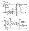
- a first detailed embodiment of a voltage regulator 54 according to the invention is shown in Fig. 5 as regulator 54a which incorporates circuit l0a.
- the path 56 from output terminal 58 of the error amplifier 60, the emitter 40 of the transistor l4a and the inverting input terminal 64 via a feedback path 70 all connect at a node 72.
- the path 70 contains resistive and capacitive elements to control the stability and bandwidth of the outer, global feedback loop.
- V ref is applied to the noninverting input terminal 62.
- the sense line 66 is connected to the inverting input terminal 64 through the attenuator 68 which comprises a voltage divider network of resistors 73 and 74.
- a resistor 76 is connected between the sense line 66 and the load path 26 to maintain stable operation of the regulator 54a in the event of an open sense line 66.
- Capacitors 80 and 8l provide known, stable impedances for both the regulator 54a and the load 28 for frequencies near and above the regulator bandwidth.
- Capacitor 82 connected to the noninverting input terminal 62 filters RF noise that otherwise may interfere with the operation of the regulator 54a.
- V out2 is sensed by the sense line 66 at a sense point remote from the MOSFET l2a and transmitted to the inverting input terminal 64 of the error amplifier 60 after appropriate attenuation.
- the error amplifier 60 senses a difference between the attenuated V out2 and the reference voltage V ref levels and generates in response an error signal at its output terminal 58.
- This error signal is routed via path 56 to the emitter 40 to form the input voltage V in .
- V in is then compared to V out appearing at the node 20 to change the voltage on gate 34 accordingly.
- V out2 thus follows the V ref .
- the voltage supply V cc to the regulator 54a can fluctuate to any level so long as it exceeds the "head room" required by the MOSFET l2a.
- a second detailed embodiment of a regulator 54 is shown in Fig. 6 as regulator 54b.
- the design of the regulator 54b is similar to that of 54a except for the following differences.
- the reference voltage V ref and sensed output voltage V out2 are summed at the inverting input terminal 64 of the error amplifier 60 and are compared with a zero reference voltage transmitted through a resistor 82 to the noninverting input terminal 62.
- Path 56 connects the output terminal 58 of amplifier 60 to the base 38 to transmit an error signal that forms V in .
- Zener diode 48 is connected between the collector 36 and the gate 34 to shift the voltage at the collector downward as it is transmitted to the gate.
- the regulator 54b also contains a protective diode 84 connected to the collector 36 to limit the maximum gate-to-source voltage of the MOSFET l2.
- a protective diode 86 limits the minimum gate-to-source voltage difference.
- the interconnections between the components of the regulator 54b enable it to sink current through the load path 26 while maintaining the sensed output voltage V out2 . substantially equal to a predetermined factor of the reference voltage V ref . Changes in V out2 are detected by the amplifier 60 and transmitted through the regulator 54b as described above to change the current drawn into the source 32 from the load 28.
Landscapes
- Engineering & Computer Science (AREA)
- Power Engineering (AREA)
- Continuous-Control Power Sources That Use Transistors (AREA)
- Amplifiers (AREA)
Applications Claiming Priority (2)
| Application Number | Priority Date | Filing Date | Title |
|---|---|---|---|
| US06/848,520 US4728901A (en) | 1986-04-07 | 1986-04-07 | Power buffer circuit |
| US848520 | 1986-04-07 |
Publications (2)
| Publication Number | Publication Date |
|---|---|
| EP0240618A2 true EP0240618A2 (de) | 1987-10-14 |
| EP0240618A3 EP0240618A3 (de) | 1988-08-31 |
Family
ID=25303513
Family Applications (1)
| Application Number | Title | Priority Date | Filing Date |
|---|---|---|---|
| EP86201845A Withdrawn EP0240618A3 (de) | 1986-04-07 | 1986-10-22 | Leistungspufferschaltung |
Country Status (3)
| Country | Link |
|---|---|
| US (1) | US4728901A (de) |
| EP (1) | EP0240618A3 (de) |
| JP (1) | JPH0736498B2 (de) |
Cited By (2)
| Publication number | Priority date | Publication date | Assignee | Title |
|---|---|---|---|---|
| GB2231179A (en) * | 1989-03-31 | 1990-11-07 | Marelli Autronica | Device for controlling and regulating a direct-current electric motor |
| GB2260045A (en) * | 1991-09-25 | 1993-03-31 | Nat Semiconductor Corp | Current source/sink MOSFET circuit |
Families Citing this family (15)
| Publication number | Priority date | Publication date | Assignee | Title |
|---|---|---|---|---|
| US4882056A (en) * | 1988-04-01 | 1989-11-21 | Pall Corporation | Fluid filter element with an overlapped wrap |
| US5187110A (en) * | 1990-10-05 | 1993-02-16 | Allied-Signal Inc. | Field effect transistor-bipolar transistor darlington pair |
| US5086282A (en) * | 1990-10-05 | 1992-02-04 | Allied-Signal Inc. | Field effect transistor-bipolar transistor Darlington pair |
| US5351242A (en) * | 1992-04-14 | 1994-09-27 | Marian Kramarczyk | Method and apparatus for configuring and maintaining token ring networks |
| US5539727A (en) * | 1992-04-14 | 1996-07-23 | Kramarczyk; Marian | Method and apparatus for configuring and maintaining token ring networks |
| US5485077A (en) * | 1993-08-09 | 1996-01-16 | Aphex Systems, Ltd. | Concentric servo voltage regulator utilizing an inner servo loop and an outer servo loop |
| US5861736A (en) * | 1994-12-01 | 1999-01-19 | Texas Instruments Incorporated | Circuit and method for regulating a voltage |
| US5612612A (en) * | 1995-12-21 | 1997-03-18 | Aphex Systems, Ltd. | Functional control block for voltage regulator with dual servo loops |
| US6547353B2 (en) | 1999-07-27 | 2003-04-15 | Stmicroelectronics, Inc. | Thermal ink jet printhead system with multiple output driver circuit for powering heating element and associated method |
| US6437956B1 (en) * | 2000-06-09 | 2002-08-20 | International Business Machines Corporation | Circuit for bipolar transistor stress and qualification |
| US7679418B2 (en) * | 2007-04-27 | 2010-03-16 | Mosaid Technologies Incorporated | Voltage level shifter and buffer using same |
| KR101153552B1 (ko) * | 2010-12-07 | 2012-06-12 | 한국과학기술원 | 선형 증폭기 |
| CA2968709C (en) | 2014-11-25 | 2021-11-02 | B Medical Systems S.A.R.L. | Cooling device |
| US10707683B2 (en) * | 2016-09-29 | 2020-07-07 | Tokitae Llc | Directing or modulating electrical power drawn by one or more loads from a solar photovoltaic module array while maintaining a buffer margin |
| JP6870403B2 (ja) * | 2017-03-16 | 2021-05-12 | セイコーエプソン株式会社 | 発振回路、回路装置、発振器、電子機器及び移動体 |
Family Cites Families (11)
| Publication number | Priority date | Publication date | Assignee | Title |
|---|---|---|---|---|
| US3244963A (en) * | 1961-11-01 | 1966-04-05 | Bausch & Lomb | Regulated power supply |
| US3315149A (en) * | 1963-09-04 | 1967-04-18 | Robert D Strait | High stability regulated voltage supply |
| US3448396A (en) * | 1966-12-21 | 1969-06-03 | Collins Radio Co | Electronic circuit-direct coupled totem pole emitter follower |
| JPS5726361B2 (de) * | 1974-04-25 | 1982-06-04 | ||
| JPS5253643A (en) * | 1975-10-29 | 1977-04-30 | Hitachi Ltd | Differential amplifier with source follower |
| JPS53128252A (en) * | 1977-04-15 | 1978-11-09 | Hitachi Ltd | Emitter follwoer circuit |
| JPS5446352A (en) * | 1977-09-21 | 1979-04-12 | Hitachi Ltd | Power source regulator circuit |
| FR2493069A1 (fr) * | 1980-10-23 | 1982-04-30 | Efcis | Amplificateur integre en classe ab en technologie cmos |
| JPS59106013A (ja) * | 1982-12-10 | 1984-06-19 | Fujitsu Ltd | 電圧安定器 |
| JPS59215121A (ja) * | 1983-05-21 | 1984-12-05 | Sony Corp | バツフア回路 |
| US4560918A (en) * | 1984-04-02 | 1985-12-24 | Rca Corporation | High-efficiency, low-voltage-drop series regulator using as its pass element an enhancement-mode FET with boosted gate voltage |
-
1986
- 1986-04-07 US US06/848,520 patent/US4728901A/en not_active Expired - Lifetime
- 1986-10-22 EP EP86201845A patent/EP0240618A3/de not_active Withdrawn
-
1987
- 1987-03-27 JP JP62073966A patent/JPH0736498B2/ja not_active Expired - Fee Related
Cited By (3)
| Publication number | Priority date | Publication date | Assignee | Title |
|---|---|---|---|---|
| GB2231179A (en) * | 1989-03-31 | 1990-11-07 | Marelli Autronica | Device for controlling and regulating a direct-current electric motor |
| GB2260045A (en) * | 1991-09-25 | 1993-03-31 | Nat Semiconductor Corp | Current source/sink MOSFET circuit |
| US5381082A (en) * | 1991-09-25 | 1995-01-10 | National Semiconductor Corporation | High-speed, fully-isolated current source/sink |
Also Published As
| Publication number | Publication date |
|---|---|
| JPH0736498B2 (ja) | 1995-04-19 |
| EP0240618A3 (de) | 1988-08-31 |
| JPS62239607A (ja) | 1987-10-20 |
| US4728901A (en) | 1988-03-01 |
Similar Documents
| Publication | Publication Date | Title |
|---|---|---|
| US4728901A (en) | Power buffer circuit | |
| US6407537B2 (en) | Voltage regulator provided with a current limiter | |
| US5506544A (en) | Bias circuit for depletion mode field effect transistors | |
| KR101288316B1 (ko) | 선형 조정기 및 그 방법 | |
| US5548205A (en) | Method and circuit for control of saturation current in voltage regulators | |
| US4008441A (en) | Current amplifier | |
| US6566954B2 (en) | High frequency amplifier bias circuit, high frequency power amplifier, and communication device | |
| US5982236A (en) | High-frequency power amplifier | |
| US4038607A (en) | Complementary field effect transistor amplifier | |
| US20020093316A1 (en) | Linear regulator enhancement technique | |
| JP2003223232A (ja) | 電流源回路 | |
| US4442408A (en) | Differential amplifier with auto bias adjust | |
| US6747508B2 (en) | Resistance mirror circuit | |
| US4612514A (en) | Feedback amplifier | |
| KR100580748B1 (ko) | 게이트 바이어싱 장치 | |
| US10778111B1 (en) | Voltage controlled adjustable current source | |
| US7486143B2 (en) | Circuit for biasing a transistor and related system and method | |
| US4847566A (en) | CMOS Amplifier having enhanced current sinking and capacitance load drive | |
| US7230492B2 (en) | Robust monolithic automatic bias circuit with current setting apparatus | |
| US6100753A (en) | Bias stabilization circuit | |
| US4560948A (en) | Circuit for increasing voltage gain | |
| US4912431A (en) | Control amplifier | |
| US10848142B2 (en) | Constant resistance input pass switch with overvoltage protection | |
| US5939943A (en) | Amplifier with improved output voltage swing | |
| US20250125773A1 (en) | Radio frequency circuit providing temperature compensation |
Legal Events
| Date | Code | Title | Description |
|---|---|---|---|
| PUAI | Public reference made under article 153(3) epc to a published international application that has entered the european phase |
Free format text: ORIGINAL CODE: 0009012 |
|
| AK | Designated contracting states |
Kind code of ref document: A2 Designated state(s): DE FR GB NL |
|
| PUAL | Search report despatched |
Free format text: ORIGINAL CODE: 0009013 |
|
| AK | Designated contracting states |
Kind code of ref document: A3 Designated state(s): DE FR GB NL |
|
| 17P | Request for examination filed |
Effective date: 19880926 |
|
| 17Q | First examination report despatched |
Effective date: 19900824 |
|
| STAA | Information on the status of an ep patent application or granted ep patent |
Free format text: STATUS: THE APPLICATION IS DEEMED TO BE WITHDRAWN |
|
| 18D | Application deemed to be withdrawn |
Effective date: 19961228 |
|
| RIN1 | Information on inventor provided before grant (corrected) |
Inventor name: PEPPER, STEVEN H. |