EP0232184B1 - Infrared detector - Google Patents
Infrared detector Download PDFInfo
- Publication number
- EP0232184B1 EP0232184B1 EP87301053A EP87301053A EP0232184B1 EP 0232184 B1 EP0232184 B1 EP 0232184B1 EP 87301053 A EP87301053 A EP 87301053A EP 87301053 A EP87301053 A EP 87301053A EP 0232184 B1 EP0232184 B1 EP 0232184B1
- Authority
- EP
- European Patent Office
- Prior art keywords
- infrared
- substrate
- dielectric layer
- layer
- cold shield
- Prior art date
- Legal status (The legal status is an assumption and is not a legal conclusion. Google has not performed a legal analysis and makes no representation as to the accuracy of the status listed.)
- Expired - Lifetime
Links
Images
Classifications
-
- H—ELECTRICITY
- H10—SEMICONDUCTOR DEVICES; ELECTRIC SOLID-STATE DEVICES NOT OTHERWISE PROVIDED FOR
- H10F—INORGANIC SEMICONDUCTOR DEVICES SENSITIVE TO INFRARED RADIATION, LIGHT, ELECTROMAGNETIC RADIATION OF SHORTER WAVELENGTH OR CORPUSCULAR RADIATION
- H10F77/00—Constructional details of devices covered by this subclass
- H10F77/30—Coatings
- H10F77/306—Coatings for devices having potential barriers
- H10F77/331—Coatings for devices having potential barriers for filtering or shielding light, e.g. multicolour filters for photodetectors
- H10F77/334—Coatings for devices having potential barriers for filtering or shielding light, e.g. multicolour filters for photodetectors for shielding light, e.g. light blocking layers or cold shields for infrared detectors
-
- H—ELECTRICITY
- H10—SEMICONDUCTOR DEVICES; ELECTRIC SOLID-STATE DEVICES NOT OTHERWISE PROVIDED FOR
- H10F—INORGANIC SEMICONDUCTOR DEVICES SENSITIVE TO INFRARED RADIATION, LIGHT, ELECTROMAGNETIC RADIATION OF SHORTER WAVELENGTH OR CORPUSCULAR RADIATION
- H10F77/00—Constructional details of devices covered by this subclass
- H10F77/40—Optical elements or arrangements
- H10F77/413—Optical elements or arrangements directly associated or integrated with the devices, e.g. back reflectors
Definitions
- the present invention relates to an infrared detector, more particularly, it relates to a structure of a cold shield for an infrared detector array.
- Infrared images are detected by an infrared detector of an imaging system.
- the infrared detector comprises an infrared detector array and an infrared shielding device, which absorbs infrared radiation (below, "infrared") and is fully cooled so that the shielding device does not become an infrared emitting source. Since the infrared shielding device is cooled, it is known as a cold shield.
- the cold shield excludes unnecessary and undesired infrared, and necessary and desired infrared to be detected is allowed to pass through the cold shield, whereby the infrared image to be detected is accurately detected by the detector array.
- infrared reflected by an electrode of a detector element in an array is reflected by optical parts and then sometimes impinges on the detecting area. Thus, the detection accuracy for the infrared is lowered. This phenomenon is known as optical crosstalk.
- JP-A-60 198774 by the present applicant discloses an infrared ray detector having the features of the preamble of accompanying claim 1.
- An embodiment of the present invention may provide an infrared detector of an imaging system wherein an infrared image can be accurately detected.
- An embodiment of the present invention may provide an infrared detector having a cold shield wherein infrared rays absorbed in the cold shield are not emitted therefrom.
- an embodiment of the present invention may provide an infrared detector having openings in a cold shield, through which openings only necessary and desired infrared rays are allowed to pass.
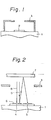
- Figure 1 is a schematic cross-sectional view of a previously proposed infrared detector, and as shown in Fig.1, an infrared detector array 2, which detects an infrared image, is provided on a cold stage 1 which is cooled by, for example, liquid nitrogen. Further, a cold shield 3 is also provided on the cold stage 1 so that unnecessary and undesired infrared rays are shielded, and necessary and desired infrared rays are passed therethrough to lead the infrared to detector array 2.
- the cold shield 3 is made of aluminium having, for example, a black surface.
- the cold shield 3 absorbs the infrared (infrared radiation) and is fully cooled by a cooling device (not shown) at the cold stage 1 so that the cold shield 3 does not become an infrared emitting source.
- the cold shield 3 excludes unnecessary and undesired infrared.
- the detector array by leading only infrared passed through an opening of the cold shield to the detector array, an accurate detection of the infrared image is obtained.
- infrared rays 8 directly impinge on a detective (detecting) area 4, and infrared rays allowed to impinge on the detector array 2 through a window 7 are detected by the detective area 4.
- infrared rays 9 impinging on the electrodes 6 are reflected by the electrodes 6 so that the reflected infrared rays are reflected by the window 7, etc., and often impinge on, for example, another detective area 5, whereby the accuracy of the infrared detection is lowered.
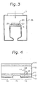
- Figure 3 shows a schematic cross-sectional view of an embodiment of the present invention.
- an infrared detector comprising a cold shield 20 and infrared detector array 21 is provided on the cold stage 1, and spacers 25 are arranged between the cold shield and the infrared detector array 21.
- a light (i.e. infrared) shielding portion 16 of the cold shield consists of five layers; i.e. a dielectric layer 14, a substrate 10, an infrared absorbing layer 11 formed on one surface of the substrate 10, a dielectric layer 12 formed on the infrared absorbing layer 11, and an infrared reflecting layer 13 formed on the dielectric layer 12.
- the substrate 10 is made of an infrared penetrating (transmitting) material, for example, ZnS, ZnSe, and Ge, etc.
- the infrared absorbing layer 11 is made of, for example, Cr or Ni, etc.
- the dielectric layer is made of, for example, CeF3 or PbF2 etc.
- the infrared reflecting layer 13 is made of a metal such as Al or Au, etc.
- the light shielding portion 16 of the cold shield efficiently eliminates infrared rays by absorbing them and causing destructive interference when they impinge on the portion 16.
- the present invention is effective even without the dielectric layer 14.
- An opening portion (transmitting portion) 15 of the cold shield consists of three layers, i.e. the dielectric layer 14, the substrate 10, and the dielectric layer 12.
- Infrared rays impinging thereon from above are efficiently passed through the opening portion 15 of the cold shield, so that they are led to a detective area (not shown).
- the opening portion 15 of the cold shield is formed by the substrate 10 made of an infrared transmitting material and the dielectric layer 12, which have a proper refractive index for giving a good optical transmission property, the infrared rays impinging on the opening portion 15 can be efficiently led to a detective area.
- part of the infrared 17 impinging on the light shielding portion 16 is reflected at the interface between the substrate 10 and the infrared absorbing layer 11, due to the difference between the refractive indices n1 and n2 thereof.
- the part of the infrared reflected at the interface is designated 18 in Fig.4.
- This infrared reflected at the surface of the infrared reflecting layer 13 passes through the dielectric layer 12 again and is partly absorbed by the infrared absorbing layer 11, the rest being emitted from the infrared absorbing layer 11.
- the emitted infrared is designated 19.
- the infrared 18 and 19 are mutually cancelled and thus the emission of infrared from the light shielding portion 16 is prevented.
- the regulation of the intensity of the infrared 18 and 19 can be carried out by selecting the material and the thickness of the infrared absorbing layer 11. Further, regulation of the phase difference between the infrared 18 and 19 can be carried out by adjusting of the thickness of the dielectric layer 12.
- the thickness of the dielectric layers in the opening portion and the light receiving portion 16 may be made the same thickness, the cold shield can be produced advantageously.
- a substrate 10 of ZnS having a thickness of 200 to 500 ⁇ m, an absorbing layer of Cr having a thickness of about 0.05 ⁇ m, and an absorbing layer 13 of Al having a thickness of about 1 ⁇ m are used.
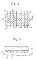
- Figure 5 shows a plan view of a cold shield provided on a detector array embodying the present invention
- Figure 6 shows a cross-sectional view taken along a line A-A' of Fig.5.
- the light shielding portion 16 of the cold shield 20 shields all portions except for the detective area 22.
- the opening portion 15 of the cold shield 20 is provided just above the detective area 22.
- infrared impinging on the opening portion 15 is led only to the detective area 22 just below the opening portion 15.
- infrared impinging on the light shielding portion 16 is eliminated by the absorbing effect and interference action of the light shielding portion 16, the problem of undesired infrared reaching another detective area because of reflection at the electrode-23, etc., as explained for the related art, does not occur.
Landscapes
- Photometry And Measurement Of Optical Pulse Characteristics (AREA)
- Radiation Pyrometers (AREA)
- Solid State Image Pick-Up Elements (AREA)
Applications Claiming Priority (2)
| Application Number | Priority Date | Filing Date | Title |
|---|---|---|---|
| JP25019/86 | 1986-02-07 | ||
| JP61025019A JPS62201325A (ja) | 1986-02-07 | 1986-02-07 | 赤外線検知器 |
Publications (3)
| Publication Number | Publication Date |
|---|---|
| EP0232184A2 EP0232184A2 (en) | 1987-08-12 |
| EP0232184A3 EP0232184A3 (en) | 1989-06-07 |
| EP0232184B1 true EP0232184B1 (en) | 1992-12-23 |
Family
ID=12154193
Family Applications (1)
| Application Number | Title | Priority Date | Filing Date |
|---|---|---|---|
| EP87301053A Expired - Lifetime EP0232184B1 (en) | 1986-02-07 | 1987-02-06 | Infrared detector |
Country Status (5)
| Country | Link |
|---|---|
| US (1) | US4795907A (OSRAM) |
| EP (1) | EP0232184B1 (OSRAM) |
| JP (1) | JPS62201325A (OSRAM) |
| KR (1) | KR900005916B1 (OSRAM) |
| DE (1) | DE3783144T2 (OSRAM) |
Families Citing this family (28)
| Publication number | Priority date | Publication date | Assignee | Title |
|---|---|---|---|---|
| JPH01164073A (ja) * | 1987-09-11 | 1989-06-28 | Canon Inc | 光電変換装置 |
| US4814620A (en) * | 1987-12-01 | 1989-03-21 | Honeywell Inc. | Tilted array with parallel cold shield |
| US4812653A (en) * | 1987-12-01 | 1989-03-14 | Honeywell Inc. | Sharp edge for thick coatings |
| US4812655A (en) * | 1987-12-09 | 1989-03-14 | Honeywell Inc. | Prism cold shield |
| FR2651315B1 (fr) * | 1989-08-22 | 1991-11-15 | Detecteurs Infra Rouges Ste Fs | Dispositif de detection infra-rouge. |
| US5089705A (en) * | 1990-02-16 | 1992-02-18 | Fujitsu Limited | Infrared detector having dewar with film coatings to suppress reflections |
| US5277782A (en) * | 1991-12-13 | 1994-01-11 | Optical Radiation Corporation | Baffled cold shields for infrared detector |
| JP2783238B2 (ja) * | 1996-02-09 | 1998-08-06 | 日本電気株式会社 | Ir信号通信装置 |
| US6374255B1 (en) * | 1996-05-21 | 2002-04-16 | Immersion Corporation | Haptic authoring |
| US6256011B1 (en) * | 1997-12-03 | 2001-07-03 | Immersion Corporation | Multi-function control device with force feedback |
| DE19842403B4 (de) * | 1998-09-16 | 2004-05-06 | Braun Gmbh | Strahlungssensor mit mehreren Sensorelementen |
| US6693626B1 (en) * | 1999-12-07 | 2004-02-17 | Immersion Corporation | Haptic feedback using a keyboard device |
| US6904823B2 (en) * | 2002-04-03 | 2005-06-14 | Immersion Corporation | Haptic shifting devices |
| AU2003285886A1 (en) | 2002-10-15 | 2004-05-04 | Immersion Corporation | Products and processes for providing force sensations in a user interface |
| GB2418475B (en) * | 2003-06-09 | 2007-10-24 | Immersion Corp | Interactive gaming systems with haptic feedback |
| JP5368847B2 (ja) * | 2009-03-26 | 2013-12-18 | パナソニック株式会社 | 赤外線放射素子 |
| US8692172B2 (en) * | 2009-04-21 | 2014-04-08 | Raytheon Company | Cold shield apparatus and methods |
| US9104791B2 (en) * | 2009-05-28 | 2015-08-11 | Immersion Corporation | Systems and methods for editing a model of a physical system for a simulation |
| US9466335B2 (en) | 2011-04-28 | 2016-10-11 | Entrotech, Inc. | Hermetic hard disk drives comprising integrally molded filters and related methods |
| US9190115B2 (en) * | 2011-04-28 | 2015-11-17 | Entrotech, Inc. | Method of assembling a disk drive |
| JP6003605B2 (ja) * | 2012-12-12 | 2016-10-05 | Tdk株式会社 | 赤外線検知装置 |
| US9866924B2 (en) | 2013-03-14 | 2018-01-09 | Immersion Corporation | Systems and methods for enhanced television interaction |
| WO2015164551A1 (en) | 2014-04-22 | 2015-10-29 | Entrotech, Inc. | Re-workable sealed hard disk drives, cover seals therefor, and related methods |
| US10002645B2 (en) | 2014-06-09 | 2018-06-19 | Entrotech, Inc. | Laminate-wrapped hard disk drives and related methods |
| US9601161B2 (en) | 2015-04-15 | 2017-03-21 | entroteech, inc. | Metallically sealed, wrapped hard disk drives and related methods |
| US10636777B2 (en) * | 2017-12-22 | 2020-04-28 | Ams Sensors Uk Limited | Infra-red device |
| US20230250292A1 (en) * | 2020-07-29 | 2023-08-10 | Dow Global Technologies Llc | Aromatic hydrocarbon-soluble anthraquinone |
| CN116479389B (zh) * | 2023-05-19 | 2025-09-12 | 中航凯迈(上海)红外科技有限公司 | 一种中波红外焦平面探测器冷屏内表面的处理方法 |
Family Cites Families (7)
| Publication number | Priority date | Publication date | Assignee | Title |
|---|---|---|---|---|
| US3963926A (en) * | 1975-01-09 | 1976-06-15 | Texas Instruments Incorporated | Detector cold shield |
| US4179181A (en) * | 1978-04-03 | 1979-12-18 | American Optical Corporation | Infrared reflecting articles |
| FR2487512A1 (fr) * | 1980-07-22 | 1982-01-29 | Thomson Csf | Dispositif detecteur de rayonnement infrarouge |
| US4431918A (en) * | 1981-03-27 | 1984-02-14 | Honeywell Inc. | Etchable glass cold shield for background limited detectors |
| US4446372A (en) * | 1981-07-01 | 1984-05-01 | Honeywell Inc. | Detector cold shield |
| JPS60195502A (ja) * | 1984-03-19 | 1985-10-04 | Canon Inc | 金属回転多面鏡 |
| FR2577073B1 (fr) * | 1985-02-06 | 1987-09-25 | Commissariat Energie Atomique | Dispositif matriciel de detection d'un rayonnement lumineux a ecrans froids individuels integres dans un substrat et son procede de fabrication |
-
1986
- 1986-02-07 JP JP61025019A patent/JPS62201325A/ja active Granted
-
1987
- 1987-02-06 DE DE8787301053T patent/DE3783144T2/de not_active Expired - Fee Related
- 1987-02-06 KR KR1019870000959A patent/KR900005916B1/ko not_active Expired
- 1987-02-06 US US07/011,536 patent/US4795907A/en not_active Expired - Fee Related
- 1987-02-06 EP EP87301053A patent/EP0232184B1/en not_active Expired - Lifetime
Also Published As
| Publication number | Publication date |
|---|---|
| DE3783144T2 (de) | 1993-04-22 |
| JPS62201325A (ja) | 1987-09-05 |
| KR870008175A (ko) | 1987-09-24 |
| DE3783144D1 (de) | 1993-02-04 |
| JPH0453369B2 (OSRAM) | 1992-08-26 |
| EP0232184A3 (en) | 1989-06-07 |
| US4795907A (en) | 1989-01-03 |
| KR900005916B1 (ko) | 1990-08-16 |
| EP0232184A2 (en) | 1987-08-12 |
Similar Documents
| Publication | Publication Date | Title |
|---|---|---|
| EP0232184B1 (en) | Infrared detector | |
| EP0187412B1 (en) | Monochromatic cathode ray tube | |
| CA1154881A (en) | Apparatus for detecting the location of incident radiation | |
| US4865405A (en) | Optical filter | |
| US5119232A (en) | Infrared-transmissive optical window | |
| US4446372A (en) | Detector cold shield | |
| US6655675B2 (en) | X-ray detector offering an improved light yield | |
| EP0041146B1 (en) | Method and apparatus for determination of angle incidence of electromagnetic energy | |
| EP0169966B1 (en) | Radiation image read-out apparatus | |
| US4739168A (en) | X-ray detector and method for manufacturing the same | |
| EP0299646A2 (en) | Improved method and apparatus for sensing or determining one or more properties or the identity of a sample | |
| EP0272689B1 (en) | Cathode ray tube with reflection prevention film | |
| US20020150204A1 (en) | X-ray phase contrast imaging using a fabry-perot interferometer concept | |
| EP0169965B1 (en) | Radiation image read-out apparatus | |
| GB2218875A (en) | Thermal imager | |
| US20250271302A1 (en) | Integrated spectral imaging device with reduced crosstalk | |
| US6392782B1 (en) | Photonic band gap dual-spectrum sensor | |
| JPH0915040A (ja) | 焦電型赤外線検出器 | |
| JPH06273232A (ja) | 測色計の受光光学系 | |
| US5015857A (en) | Infrared detector | |
| US4306762A (en) | Reflecting apparatus in an optical system | |
| US4195223A (en) | Apparatus for optically scanning a surface | |
| US7042000B2 (en) | Radiation image read-out apparatus and stimulating light cut filter | |
| US5103100A (en) | X-ray detector | |
| JPH0716016B2 (ja) | 赤外線検知素子 |
Legal Events
| Date | Code | Title | Description |
|---|---|---|---|
| PUAI | Public reference made under article 153(3) epc to a published international application that has entered the european phase |
Free format text: ORIGINAL CODE: 0009012 |
|
| AK | Designated contracting states |
Kind code of ref document: A2 Designated state(s): DE FR GB |
|
| PUAL | Search report despatched |
Free format text: ORIGINAL CODE: 0009013 |
|
| AK | Designated contracting states |
Kind code of ref document: A3 Designated state(s): DE FR GB |
|
| 17P | Request for examination filed |
Effective date: 19890810 |
|
| 17Q | First examination report despatched |
Effective date: 19901102 |
|
| GRAA | (expected) grant |
Free format text: ORIGINAL CODE: 0009210 |
|
| AK | Designated contracting states |
Kind code of ref document: B1 Designated state(s): DE FR GB |
|
| REF | Corresponds to: |
Ref document number: 3783144 Country of ref document: DE Date of ref document: 19930204 |
|
| ET | Fr: translation filed | ||
| PLBE | No opposition filed within time limit |
Free format text: ORIGINAL CODE: 0009261 |
|
| STAA | Information on the status of an ep patent application or granted ep patent |
Free format text: STATUS: NO OPPOSITION FILED WITHIN TIME LIMIT |
|
| 26N | No opposition filed | ||
| PGFP | Annual fee paid to national office [announced via postgrant information from national office to epo] |
Ref country code: GB Payment date: 19980128 Year of fee payment: 12 |
|
| PGFP | Annual fee paid to national office [announced via postgrant information from national office to epo] |
Ref country code: FR Payment date: 19980210 Year of fee payment: 12 |
|
| PGFP | Annual fee paid to national office [announced via postgrant information from national office to epo] |
Ref country code: DE Payment date: 19980213 Year of fee payment: 12 |
|
| PG25 | Lapsed in a contracting state [announced via postgrant information from national office to epo] |
Ref country code: GB Free format text: LAPSE BECAUSE OF NON-PAYMENT OF DUE FEES Effective date: 19990206 |
|
| GBPC | Gb: european patent ceased through non-payment of renewal fee |
Effective date: 19990206 |
|
| PG25 | Lapsed in a contracting state [announced via postgrant information from national office to epo] |
Ref country code: FR Free format text: LAPSE BECAUSE OF NON-PAYMENT OF DUE FEES Effective date: 19991029 |
|
| PG25 | Lapsed in a contracting state [announced via postgrant information from national office to epo] |
Ref country code: DE Free format text: LAPSE BECAUSE OF NON-PAYMENT OF DUE FEES Effective date: 19991201 |
|
| REG | Reference to a national code |
Ref country code: FR Ref legal event code: ST |