EP0226050A1 - Procédé de montage d'un circuit intégré sur un substrat - Google Patents
Procédé de montage d'un circuit intégré sur un substrat Download PDFInfo
- Publication number
- EP0226050A1 EP0226050A1 EP86115782A EP86115782A EP0226050A1 EP 0226050 A1 EP0226050 A1 EP 0226050A1 EP 86115782 A EP86115782 A EP 86115782A EP 86115782 A EP86115782 A EP 86115782A EP 0226050 A1 EP0226050 A1 EP 0226050A1
- Authority
- EP
- European Patent Office
- Prior art keywords
- frame
- substrate
- conductor
- strips
- adhesive
- Prior art date
- Legal status (The legal status is an assumption and is not a legal conclusion. Google has not performed a legal analysis and makes no representation as to the accuracy of the status listed.)
- Granted
Links
Images

Classifications
-
- H—ELECTRICITY
- H01—ELECTRIC ELEMENTS
- H01L—SEMICONDUCTOR DEVICES NOT COVERED BY CLASS H10
- H01L24/00—Arrangements for connecting or disconnecting semiconductor or solid-state bodies; Methods or apparatus related thereto
- H01L24/01—Means for bonding being attached to, or being formed on, the surface to be connected, e.g. chip-to-package, die-attach, "first-level" interconnects; Manufacturing methods related thereto
- H01L24/50—Tape automated bonding [TAB] connectors, i.e. film carriers; Manufacturing methods related thereto
-
- H—ELECTRICITY
- H01—ELECTRIC ELEMENTS
- H01L—SEMICONDUCTOR DEVICES NOT COVERED BY CLASS H10
- H01L24/00—Arrangements for connecting or disconnecting semiconductor or solid-state bodies; Methods or apparatus related thereto
- H01L24/80—Methods for connecting semiconductor or other solid state bodies using means for bonding being attached to, or being formed on, the surface to be connected
- H01L24/81—Methods for connecting semiconductor or other solid state bodies using means for bonding being attached to, or being formed on, the surface to be connected using a bump connector
-
- H—ELECTRICITY
- H01—ELECTRIC ELEMENTS
- H01L—SEMICONDUCTOR DEVICES NOT COVERED BY CLASS H10
- H01L24/00—Arrangements for connecting or disconnecting semiconductor or solid-state bodies; Methods or apparatus related thereto
- H01L24/80—Methods for connecting semiconductor or other solid state bodies using means for bonding being attached to, or being formed on, the surface to be connected
- H01L24/86—Methods for connecting semiconductor or other solid state bodies using means for bonding being attached to, or being formed on, the surface to be connected using tape automated bonding [TAB]
-
- H—ELECTRICITY
- H05—ELECTRIC TECHNIQUES NOT OTHERWISE PROVIDED FOR
- H05K—PRINTED CIRCUITS; CASINGS OR CONSTRUCTIONAL DETAILS OF ELECTRIC APPARATUS; MANUFACTURE OF ASSEMBLAGES OF ELECTRICAL COMPONENTS
- H05K3/00—Apparatus or processes for manufacturing printed circuits
- H05K3/30—Assembling printed circuits with electric components, e.g. with resistor
- H05K3/32—Assembling printed circuits with electric components, e.g. with resistor electrically connecting electric components or wires to printed circuits
- H05K3/321—Assembling printed circuits with electric components, e.g. with resistor electrically connecting electric components or wires to printed circuits by conductive adhesives
-
- H—ELECTRICITY
- H01—ELECTRIC ELEMENTS
- H01L—SEMICONDUCTOR DEVICES NOT COVERED BY CLASS H10
- H01L2224/00—Indexing scheme for arrangements for connecting or disconnecting semiconductor or solid-state bodies and methods related thereto as covered by H01L24/00
- H01L2224/80—Methods for connecting semiconductor or other solid state bodies using means for bonding being attached to, or being formed on, the surface to be connected
- H01L2224/81—Methods for connecting semiconductor or other solid state bodies using means for bonding being attached to, or being formed on, the surface to be connected using a bump connector
- H01L2224/818—Bonding techniques
- H01L2224/81801—Soldering or alloying
-
- H—ELECTRICITY
- H01—ELECTRIC ELEMENTS
- H01L—SEMICONDUCTOR DEVICES NOT COVERED BY CLASS H10
- H01L2924/00—Indexing scheme for arrangements or methods for connecting or disconnecting semiconductor or solid-state bodies as covered by H01L24/00
- H01L2924/01—Chemical elements
- H01L2924/01005—Boron [B]
-
- H—ELECTRICITY
- H01—ELECTRIC ELEMENTS
- H01L—SEMICONDUCTOR DEVICES NOT COVERED BY CLASS H10
- H01L2924/00—Indexing scheme for arrangements or methods for connecting or disconnecting semiconductor or solid-state bodies as covered by H01L24/00
- H01L2924/01—Chemical elements
- H01L2924/01076—Osmium [Os]
-
- H—ELECTRICITY
- H01—ELECTRIC ELEMENTS
- H01L—SEMICONDUCTOR DEVICES NOT COVERED BY CLASS H10
- H01L2924/00—Indexing scheme for arrangements or methods for connecting or disconnecting semiconductor or solid-state bodies as covered by H01L24/00
- H01L2924/10—Details of semiconductor or other solid state devices to be connected
- H01L2924/11—Device type
- H01L2924/14—Integrated circuits
-
- H—ELECTRICITY
- H05—ELECTRIC TECHNIQUES NOT OTHERWISE PROVIDED FOR
- H05K—PRINTED CIRCUITS; CASINGS OR CONSTRUCTIONAL DETAILS OF ELECTRIC APPARATUS; MANUFACTURE OF ASSEMBLAGES OF ELECTRICAL COMPONENTS
- H05K2201/00—Indexing scheme relating to printed circuits covered by H05K1/00
- H05K2201/10—Details of components or other objects attached to or integrated in a printed circuit board
- H05K2201/10227—Other objects, e.g. metallic pieces
- H05K2201/10424—Frame holders
-
- H—ELECTRICITY
- H05—ELECTRIC TECHNIQUES NOT OTHERWISE PROVIDED FOR
- H05K—PRINTED CIRCUITS; CASINGS OR CONSTRUCTIONAL DETAILS OF ELECTRIC APPARATUS; MANUFACTURE OF ASSEMBLAGES OF ELECTRICAL COMPONENTS
- H05K2201/00—Indexing scheme relating to printed circuits covered by H05K1/00
- H05K2201/10—Details of components or other objects attached to or integrated in a printed circuit board
- H05K2201/10613—Details of electrical connections of non-printed components, e.g. special leads
- H05K2201/10621—Components characterised by their electrical contacts
- H05K2201/10681—Tape Carrier Package [TCP]; Flexible sheet connector
-
- H—ELECTRICITY
- H05—ELECTRIC TECHNIQUES NOT OTHERWISE PROVIDED FOR
- H05K—PRINTED CIRCUITS; CASINGS OR CONSTRUCTIONAL DETAILS OF ELECTRIC APPARATUS; MANUFACTURE OF ASSEMBLAGES OF ELECTRICAL COMPONENTS
- H05K2201/00—Indexing scheme relating to printed circuits covered by H05K1/00
- H05K2201/10—Details of components or other objects attached to or integrated in a printed circuit board
- H05K2201/10613—Details of electrical connections of non-printed components, e.g. special leads
- H05K2201/10954—Other details of electrical connections
- H05K2201/10984—Component carrying a connection agent, e.g. solder, adhesive
-
- H—ELECTRICITY
- H05—ELECTRIC TECHNIQUES NOT OTHERWISE PROVIDED FOR
- H05K—PRINTED CIRCUITS; CASINGS OR CONSTRUCTIONAL DETAILS OF ELECTRIC APPARATUS; MANUFACTURE OF ASSEMBLAGES OF ELECTRICAL COMPONENTS
- H05K2203/00—Indexing scheme relating to apparatus or processes for manufacturing printed circuits covered by H05K3/00
- H05K2203/01—Tools for processing; Objects used during processing
- H05K2203/0195—Tool for a process not provided for in H05K3/00, e.g. tool for handling objects using suction, for deforming objects, for applying local pressure
Definitions
- the present invention relates to a method according to the preamble of patent claim 1.
- a conductive adhesive for electrically connecting the conductor tracks of components carrying ICs to the conductor tracks on the substrate of a liquid crystal display cell (LC cell) is, for. B. from DE-OS 32 43 227 known.
- the present invention is based on the object of specifying a method for the application and adhesive contacting of ICs which is particularly suitable for automated production, in particular on substrates consisting of glass.
- the described direct application of conductive adhesive to the conductive tapes of the IC in the area of the frame consisting of insulating material substantially reduces the risk of undesirable conductive breaks occurring between adjacent conductive tracks or conductive tapes due to the conductive adhesive.
- the adhesive is applied directly by means of screen printing or a dosing syringe.
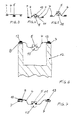
- FIG. 1 first shows a film with ICs known per se, a section of which is shown.
- the film 1 consists of an insulating material and expediently has markings 2 on the edge, e.g. B. in the form of breakthroughs that are in exact geometric relationship to the IC's on the film.
- This film has a plurality of ICs in a row, which are arranged above openings 9 in the film and are held on the film by means of conductor strips 4.
- the free ends 3 of the conductor strips 4 are attached to the film 1.
- the IC's 5 can be machine-processed in a simple manner.
- the part shown in FIG. 2 is punched out in accordance with the punched edges 6.
- This part shows the IC 5 in the opening 9, which is now held in a frame 7 by the ribbon 4.
- the parts of the conductor strips located on the frame 7 are designated by 8.
- FIGS. 3, 4 and 5 show different possibilities of how the IC 5 can be suspended in a self-supporting manner within the frame by the conductor strips 4.
- the IC 5 is located on the plane of the frame 7 and the ribbons 4 run essentially in a straight line.
- the IC 5 is again in the plane of the frame 7, but the conductor strips 4 are fastened to the lower surface of the frame 7, and the strips 4 run cranked.
- the ribbons 4 are bonded in a known manner to the corresponding location on the IC 5.
- 11 shows the bond bumps. The bond points are mechanically relieved by a plastic encapsulation 10.
- FIG. 5 shows an exemplary embodiment in which the IC 5 is located within the plane of the frame 7.
- the tapes 4 are in turn cranked and the bond points are mechanically relieved via a plastic encapsulation 10.
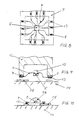
- Figure 6 now shows a method step according to the invention, in which the frame 7 is held by a pneumatic suction tool 12, in such a way that the free surface of the frame 7 is sucked in and the ends 8 of the conductor strips 4 on the Are top of the frame 7, the tool 12 holding the arrangement so that the ends 8 on the surface of the frame 7 are freely accessible from above.
- On these ends 8 is now either Screen printing or with a metering syringe in a precisely metered amount and size of adhesive conductive adhesive 13 applied.
- the other parts are denoted by the same numbers as in the other figures.
- this frame with the correspondingly mounted IC 5 and the applied adhesive spots 13 is shown again in cross section without the tool 12.
- FIG. 8 the same part is shown from above in the top view and one can see the applied adhesive spots 13 made of conductive adhesive, which are only located on the surface parts 8 of the conductor strips, which are arranged on the surface of the insulating frame 7.
- FIG. 9 now shows that is applied to a glass substrate 14 of an LC cell.
- the substrate 14 is preferably a corresponding glass plate of an LC cell and carries conductor tracks 15 which are led out of the LC cell as electrical leads.
- the tool 12 is in an upside-down state, so that the Klestoff points 13 on the conductor strips 4 now point downward.
- the tool 12 now presses this arrangement with the adhesive points 13 onto the substrate 14 in such a way that the adhesive points 13 are pressed onto the conductor tracks 15 and glued on. Since the adhesive is a conductive adhesive, an electrical contact is produced at the same time, which, after the adhesive has hardened, also forms a firm anchorage of the IC.
- FIG. 10 again shows a substrate 14 made of glass with the conductor tracks 15, on which the IC 5 is glued in the manner described above.
- a further plastic encapsulation 16 made of insulating material can further relieve the mechanical stress on the bond points and increase shock protection for the structure.
- the ICs represent integrated control circuits for the LC cell.
Landscapes
- Engineering & Computer Science (AREA)
- Microelectronics & Electronic Packaging (AREA)
- Computer Hardware Design (AREA)
- Power Engineering (AREA)
- Manufacturing & Machinery (AREA)
- Wire Bonding (AREA)
- Die Bonding (AREA)
Applications Claiming Priority (2)
| Application Number | Priority Date | Filing Date | Title |
|---|---|---|---|
| DE3543643 | 1985-12-11 | ||
| DE19853543643 DE3543643A1 (de) | 1985-12-11 | 1985-12-11 | Verfahren zum aufbringen eines ic auf ein substrat |
Publications (2)
| Publication Number | Publication Date |
|---|---|
| EP0226050A1 true EP0226050A1 (fr) | 1987-06-24 |
| EP0226050B1 EP0226050B1 (fr) | 1990-06-27 |
Family
ID=6288111
Family Applications (1)
| Application Number | Title | Priority Date | Filing Date |
|---|---|---|---|
| EP86115782A Expired - Lifetime EP0226050B1 (fr) | 1985-12-11 | 1986-11-13 | Procédé de montage d'un circuit intégré sur un substrat |
Country Status (2)
| Country | Link |
|---|---|
| EP (1) | EP0226050B1 (fr) |
| DE (2) | DE3543643A1 (fr) |
Cited By (1)
| Publication number | Priority date | Publication date | Assignee | Title |
|---|---|---|---|---|
| EP0408272A2 (fr) * | 1989-07-11 | 1991-01-16 | The Welding Institute | Liaison de conducteurs électriques |
Citations (4)
| Publication number | Priority date | Publication date | Assignee | Title |
|---|---|---|---|---|
| US4300715A (en) * | 1977-09-01 | 1981-11-17 | The Jade Corporation | Mechanical pulse reflow bonding process |
| EP0103889A2 (fr) * | 1982-09-20 | 1984-03-28 | Siemens Aktiengesellschaft | Procédé et dispositif pour le montage sur film de circuits intégrés individuels (micropacks) |
| FR2535110A1 (fr) * | 1982-10-20 | 1984-04-27 | Radiotechnique Compelec | Procede d'encapsulation d'un composant semi-conducteur dans un circuit electronique realise sur substrat et application aux circuits integres rapides |
| EP0111734A2 (fr) * | 1982-11-23 | 1984-06-27 | Licentia Patent-Verwaltungs-GmbH | Procédé de fabrication d'un dispostif d'affichage à cristal liquide |
-
1985
- 1985-12-11 DE DE19853543643 patent/DE3543643A1/de not_active Withdrawn
-
1986
- 1986-11-13 DE DE8686115782T patent/DE3672330D1/de not_active Expired - Fee Related
- 1986-11-13 EP EP86115782A patent/EP0226050B1/fr not_active Expired - Lifetime
Patent Citations (4)
| Publication number | Priority date | Publication date | Assignee | Title |
|---|---|---|---|---|
| US4300715A (en) * | 1977-09-01 | 1981-11-17 | The Jade Corporation | Mechanical pulse reflow bonding process |
| EP0103889A2 (fr) * | 1982-09-20 | 1984-03-28 | Siemens Aktiengesellschaft | Procédé et dispositif pour le montage sur film de circuits intégrés individuels (micropacks) |
| FR2535110A1 (fr) * | 1982-10-20 | 1984-04-27 | Radiotechnique Compelec | Procede d'encapsulation d'un composant semi-conducteur dans un circuit electronique realise sur substrat et application aux circuits integres rapides |
| EP0111734A2 (fr) * | 1982-11-23 | 1984-06-27 | Licentia Patent-Verwaltungs-GmbH | Procédé de fabrication d'un dispostif d'affichage à cristal liquide |
Non-Patent Citations (1)
| Title |
|---|
| ELECTRONIQUE ET APPLICATIONS INDUSTRIELLES, Nr. 260, November 1978, Seiten 29-32, Paris, FR; A. ROUALET: "Microcircuits sur film KAPTON: circuits intégrés sur bande" * |
Cited By (2)
| Publication number | Priority date | Publication date | Assignee | Title |
|---|---|---|---|---|
| EP0408272A2 (fr) * | 1989-07-11 | 1991-01-16 | The Welding Institute | Liaison de conducteurs électriques |
| EP0408272A3 (en) * | 1989-07-11 | 1991-12-11 | The Welding Institute | Bonding electrical conductors |
Also Published As
| Publication number | Publication date |
|---|---|
| DE3543643A1 (de) | 1987-06-19 |
| DE3672330D1 (de) | 1990-08-02 |
| EP0226050B1 (fr) | 1990-06-27 |
Similar Documents
| Publication | Publication Date | Title |
|---|---|---|
| DE2732529C2 (de) | Gedruckte Schaltungsplatine | |
| DE2512417B2 (de) | Elektronische uhr mit elektrooptischer anzeigevorrichtung und integrierter schaltung | |
| DE4242408C2 (de) | Verfahren zum Verbinden eines Schaltkreissubstrates mit einem Halbleiterteil | |
| DE102005019553A1 (de) | Füllmassenstruktur und Verfahren für WL-CSP | |
| DE3708309A1 (de) | Chip-packung | |
| DE4028556C1 (fr) | ||
| DE19543427A1 (de) | Chipmodul | |
| DE2058104C2 (de) | Anzeigeelement mit einem Flüssigkristall | |
| EP0391024A1 (fr) | Circuit pour dispositif d'affichage | |
| EP0226050B1 (fr) | Procédé de montage d'un circuit intégré sur un substrat | |
| EP0219659B1 (fr) | Procédé pour la fabrication d'un contact à adhesion | |
| EP0953186B1 (fr) | Module de carte a puce | |
| EP0769214A1 (fr) | Procede de realisation d'une connexion electro-conductrice | |
| DE4129964C2 (de) | Verfahren zur Herstellung einer elektrisch leitenden Befestigung einer integrierten Schaltung auf einer gedruckten Schaltung | |
| DE19860716C1 (de) | Verbindungsanordnung | |
| DE3211408A1 (de) | Substrat | |
| DE3731787C2 (de) | Anordnung von mehreren IC's auf einem Bandstreifen aus Isoliermaterial | |
| DE10228152A1 (de) | Selbsthaftende flexible Reparaturschaltung | |
| DE3533993C2 (fr) | ||
| WO1998039732A2 (fr) | Module de carte a puce et carte a puce comportant ce dernier | |
| DE3149295A1 (de) | Vorrichtung zum gleichmaessigen verteilen einer hochviskosen fluessigkeit | |
| DE2534783A1 (de) | Elektrooptische anzeigeeinrichtung und verfahren zu ihrer herstellung | |
| EP1186037B1 (fr) | Module multipuce pour montage "fils sur puce" et son procede de production | |
| DE10327515A1 (de) | Substratbasiertes IC-Package | |
| EP0406764B1 (fr) | Adaptateur pour tester des circuits intégrés montés sur une pellicule |
Legal Events
| Date | Code | Title | Description |
|---|---|---|---|
| PUAI | Public reference made under article 153(3) epc to a published international application that has entered the european phase |
Free format text: ORIGINAL CODE: 0009012 |
|
| AK | Designated contracting states |
Kind code of ref document: A1 Designated state(s): CH DE FR GB LI NL |
|
| 17P | Request for examination filed |
Effective date: 19871112 |
|
| 17Q | First examination report despatched |
Effective date: 19891006 |
|
| GRAA | (expected) grant |
Free format text: ORIGINAL CODE: 0009210 |
|
| AK | Designated contracting states |
Kind code of ref document: B1 Designated state(s): CH DE FR GB LI NL |
|
| REF | Corresponds to: |
Ref document number: 3672330 Country of ref document: DE Date of ref document: 19900802 |
|
| ET | Fr: translation filed | ||
| GBT | Gb: translation of ep patent filed (gb section 77(6)(a)/1977) | ||
| PLBE | No opposition filed within time limit |
Free format text: ORIGINAL CODE: 0009261 |
|
| STAA | Information on the status of an ep patent application or granted ep patent |
Free format text: STATUS: NO OPPOSITION FILED WITHIN TIME LIMIT |
|
| 26N | No opposition filed | ||
| PGFP | Annual fee paid to national office [announced via postgrant information from national office to epo] |
Ref country code: GB Payment date: 19931021 Year of fee payment: 8 |
|
| PGFP | Annual fee paid to national office [announced via postgrant information from national office to epo] |
Ref country code: FR Payment date: 19931108 Year of fee payment: 8 |
|
| PGFP | Annual fee paid to national office [announced via postgrant information from national office to epo] |
Ref country code: DE Payment date: 19931122 Year of fee payment: 8 |
|
| PGFP | Annual fee paid to national office [announced via postgrant information from national office to epo] |
Ref country code: NL Payment date: 19931130 Year of fee payment: 8 |
|
| PGFP | Annual fee paid to national office [announced via postgrant information from national office to epo] |
Ref country code: CH Payment date: 19931221 Year of fee payment: 8 |
|
| PG25 | Lapsed in a contracting state [announced via postgrant information from national office to epo] |
Ref country code: GB Effective date: 19941113 |
|
| PG25 | Lapsed in a contracting state [announced via postgrant information from national office to epo] |
Ref country code: LI Effective date: 19941130 Ref country code: CH Effective date: 19941130 |
|
| PG25 | Lapsed in a contracting state [announced via postgrant information from national office to epo] |
Ref country code: NL Effective date: 19950601 |
|
| GBPC | Gb: european patent ceased through non-payment of renewal fee |
Effective date: 19941113 |
|
| NLV4 | Nl: lapsed or anulled due to non-payment of the annual fee | ||
| PG25 | Lapsed in a contracting state [announced via postgrant information from national office to epo] |
Ref country code: FR Effective date: 19950731 |
|
| REG | Reference to a national code |
Ref country code: CH Ref legal event code: PL |
|
| PG25 | Lapsed in a contracting state [announced via postgrant information from national office to epo] |
Ref country code: DE Effective date: 19950801 |
|
| REG | Reference to a national code |
Ref country code: FR Ref legal event code: ST |