EP0222405A2 - Processeur de données - Google Patents
Processeur de données Download PDFInfo
- Publication number
- EP0222405A2 EP0222405A2 EP86115803A EP86115803A EP0222405A2 EP 0222405 A2 EP0222405 A2 EP 0222405A2 EP 86115803 A EP86115803 A EP 86115803A EP 86115803 A EP86115803 A EP 86115803A EP 0222405 A2 EP0222405 A2 EP 0222405A2
- Authority
- EP
- European Patent Office
- Prior art keywords
- processing
- data
- address
- section
- memory
- Prior art date
- Legal status (The legal status is an assumption and is not a legal conclusion. Google has not performed a legal analysis and makes no representation as to the accuracy of the status listed.)
- Granted
Links
Images


Classifications
-
- G—PHYSICS
- G06—COMPUTING; CALCULATING OR COUNTING
- G06T—IMAGE DATA PROCESSING OR GENERATION, IN GENERAL
- G06T1/00—General purpose image data processing
- G06T1/20—Processor architectures; Processor configuration, e.g. pipelining
Definitions
- the present invention relates to a data processor.
- an image processing system which includes a processor for processing image data and a processor for processing an address of the image data (JP-A-58-215813).
- a high operation speed is required for the arithmetic operation having an operation configuration unique to the image processing; moreover, the access and the transfer of a great amount of data arranged in a 2- dimensional structure must be accomplished at a high speed.
- the pipeline system has a simple hardware structure and a simple processing control, and hence a high-speed operation can be relatively easily accomplished.
- the processing speed is substantially proportional to the switching speed of the transistor, the very high speed operation is limited.
- the processing is restricted by the pipeline structure, which leads to a problem that the flexibility of the system is reduced.
- the speed of the data transfer in the parallel system is determined by the method of combining the processor elements and the memory.
- the combining method is classified into a shared memory type and a network type. Since the image processing handles a great amount of data, the combining method of shared memory type is adopted in many systems. In the pipeline system, the processing and the transfer is mixed, and hence the speed of each stage of the pipeline must be increased.
- the high-speed image processing system enables various image processing and the contents of the image processing include not only a simple linear processing but also nonlinear processing such as a conditional branch processing; consequently, the flexible system is required.
- this system is not sufficient to organically combine a plurality of processors so as to achieve a high-speed processing and a complex calculation.
- An example of the video image processing system of Fig. 1 aims at a higher-speed data processing and comprises an input/output section 1 (IOC), a memory section 2 (VIM) including an input image memory 2A (VIMIN) and an output image memory 2B (VIMOUT), a data processing section 3 including a position invariant processor 3A (PIP) for mainly calculating a pixel value and a position variant processor 3B (PVP) for accomplishing data flow control such as the address control and for effecting the timing control, and a processor 4 (TC) as a controller of the overall system for controlling the execution of processing, termination of processing, and program exchange.
- a host computer 5 HP is connected to control the overall video image processing system.
- the IOC 1 is configured such that, for example, a video signal from a video camera 6 or a VTR is subjected to an A/D conversion to obtain a digital image data, which is then written in the VIMIN 2A; furthermore, a processed image data is read from the VIMOUT 2B and is restored into an analog video signal through a D/A conversion, which is then recorded, for example, in a VTR 7 or is supplied to a monitor image receiver 8, thereby enabling a video image to be monitored.
- signals for externally controlling the VIM 2 such as a clock, a dominant mode signal, an address, and a write control signal are supplied from the IOC 1.
- the signals which can be inputted to or outputted from the IOC 1 are signals of the NTSC system or the R/G/B system.
- the signal system is specified through the TC 4.
- a pixel is a data item comprising eight bits, for example.
- a read or write operation of the VIM 2 is achieved in a group of an image, namely, a field or frame unit.
- the VIMIN 2A and VIMOUT 2B each include a plurality of memory sheets each having a capacity of a field or frame of image data.
- 12 sheets of 768 x 512 byte frame memory are provided.
- the utilization of these 12 sheets of frame memory is not fixed, namely, the 12 sheets can be arbitrarily allocated as the VIMIN 2A or the VIMOUT 2B according to the processing purpose or the processing objective image.
- the memory sheets are designed to be used in a pair and when a sheet of a pair is in the write state, the other sheet can be used for a read operation, which enables the IOC 1 to achieve parallel processing of an external processing through the VIM 2 and the internal processing through the VIM 2 by use of the PIP 3A and the PVP 3B.
- the dominant mode signal to determine whether the sheets of frame memory of the VIM 2 are under control of the IOC 1 or the PVP 3B is generated from the IOC 1 and is supplied to the VIM 2.
- the address of digital data to be processed, the write control signal, the read mode signal, and data select signal for internally controlling the VI M 2 are supplied from the PVP 3B to the VIM 2, and then the data stored at the address is transferred to the PIP 3A for the processing thereof.
- the data processed in the PIP 3A is supplied to the VIM system 2, and then an address and other information are supplied from the PVP 3B to the VIM 2. As a result, the digital data thus processed is written in the VOM 2.
- an address and other information are also supplied from the VIM 2 to the IOC 1, which causes the digital data read as a result to be supplied to the IOC 1, and then the digital data is converted into a predetermined analog video signal through a DA conversion and other processing so as to be fed to an output terminal.
- the data processing section 3 has a processor and reads the image data stored in the VIMIN 2A according to a program of the processor and executes various kinds of data work processing thereon, and then the processed data is written in the output image memory 2B.
- the data processing section 3 is subdivided into the PIP 3A and the PVP 3B; consequently, as compared with the conventional data processing section requiring the processing time equal to the total of the processing time of these subsections, the data processing section 3 requires only the larger processing time thereof because of provisions of these subsections. Consequently, the case of this example realizes a high-speed processing which almost allows the video data processing to be executed through a realtime processing.
- the processor of the data processing section 3 includes one sheet of processor or several sheets of processors, and the microprogram contained in the microprogram memory thereof can be changed if it is required to expand the processing capability.
- the microprogram is temporarily supplied from the HC 5 to the TC 4 so as to be stored in an RAM disposed therein; and thereafter, for example, in response to a program change request from the user (by setting the pertinent switch' to ON), the microprogram is supplied from the TC 4 to each processor, thereby changing the microprogram.
- the PIP 3A and the PVP 3B each are of the same architecture and are independent processors each including a control section, an arithmetic section, a memory section, and an input/output port. These systems are respectively structured in a multiprocessor configuration comprising a plurality of unit processors in which a high-speed processing is mainly implemented according to the parallel processing scheme.
- the PIP 3A has, for example, 60 sheets of PIP processors and several sheets of subprocessors, so that the working of the image data from the VIM 2 is accomplished or the image data is generated in the PIP 3A.
- the PVP 3B includes, for example, 30 sheets of processors to control the flow of the internal image data with respect to the VIM 2, for example, to effect allocation and recovery of the image data obtained from the VIM 2 on the PIP 3A.
- the PVP 3B generates an address data and a control signal to the VIM 2 and supplies them to the VIM 2; and the PVP 3B generates the input/output control signal of the PIP 3A and other control signals and supplies them to the PIP 3A.
- the image data processing there is not only the case where the data from a frame of the input image memory 2A is processed and the processed data is written in the output image memory 2B but also a case where the data stored in a plurality of frames from a plurality sheets of frame memory is processed.
- the number of bits to be processed in the PIP 3A and the PVP 3B is 16 in the standard specification, and for the arithmetic processing of the image data processing, it is enabled to implement a processing speed at which the processing can be implemented within a frame, namely, the realtime processing can be achieved for the 1-frame image data. There exist naturally a processing which requires a processing time exceeding a frame.
- the image data processing of the PIP 3A and the PVP 3B is accomplished in synchrony with the frame. Consequently, the PVP 3B is supplied from the IOC 1 with a processing start timing signal PS synchronized with the frame.
- the PS signal is normally at a high level and is set to a low level when the processing start timing is detected.
- the PVP 3B supplies the IOC 1 with a signal OK indicating that a processing has been completed. This signal OK is outputted from the primary processor among the processors of the PVP 3B when the processing is completed, the processor controlling the timing of the processing system.
- the primary processor of the PVP 3B softwarewise detects a fact that the processing start timing signal PS from the IOC 1 is set to the low level.
- the processor starts its operation and outputs a timing signal TS by use of a program to the other processors including the PIP 3A, and then supplies an address to the VIM 2, reads an image data from the VIM 2, and performs a work processing in the PIP 3A (step 102).
- the signal OK is outputted and the processing is terminated (step 103) to wait for the next processing start timing signal PS (step 101).
- the signal PS is generated by the IOC 1 as follows.
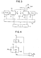
- the IOC 1 is configured as shown in Fig. 3, for example.
- the PLL circuit 11 for generating a clock generates the clock which is locked for the phase of, for example, the subcarrier of the input video signal.
- the interface 12 effects a division on the clock from the PLL circuit 11 and applies a delay on some of the resultant signals, and then the obtained signals are transmitted to the relevant sections in the IOC 1, the VIMIN 2A, and VIMOUT 2B.
- the input video signal is converted by use of a sampling clock (for example, 14.32 MHz) from the interface 12 into the digital image data in which eight bits are generated for each sampling.
- a sampling clock for example, 14.32 MHz
- the input circuit 14 is supplied with a digital image data from the A/D converter 13, and the data is transferred to the VIMIN 2A to be written therein.
- a signal specifying the signal system (NTSC or R/C/B system) is supplied from the TC 4 to the input circuit 14.
- NTSC NTSC
- R/C/B system a signal specifying the signal system
- the TC 4 TC 4 to the input circuit 14.
- NTSC NTSC
- two sheets of frame memory or exceeding two sheets
- the data is alternately written in the memory.
- the R/G/B signal six sheets of frame memory among the 12 sheets thereof are assigned as the input image memory and the data is alternately written in two sheets of frame memory for each principle color. The data is read from any frame memory for which the write operation is not conducted.
- the image data stored in the memory is separated from the IOC 1 and the data flow is then controlled by the PVP 3B.
- this input circuit 14 supplies the VIMIN 2 with only the effective signal of the image signal from which the sync signal and the burst signal portion are removed and the obtained signal is written in the frame units according to the clock delivered from the interface 12.
- the phase of the burst signal in the video signal and the phase of the clock are compared, and the output of the comparison result is supplied as a phase control signal to the PLL circuit 11.
- the clock from the PLL 11 is subjected to the phase lock operation with respect to the subcarrier in the video signal.
- a signal for extracting the burst signal, a valid/invalid signal indicating whether or not the sync signal and the burst signal portion are included in the image signal, a frame start signal FL indicating the first line of each frame, a signal indicating the vertical blanking of each field, and a video ID signal with a signal indicating the start of the line are generated and are used therein; furthermore, these signals are supplied for the processing thereof to the output circuit 15 to be described later.
- the output circuit 15 is supplied with the processed video data read from the VIMOUT 2B on the frame-by-frame basis.
- the sync signal does not include the burst signal; consequently, the output circuit 15 includes an ROM for generating a sync signal, a burst signal, and a vertical blanking signal.
- the data from the VIMOUT 2B is sent to the D/A converter together with the sync signal, the burst signal, and the vertical blanking signal (after being rearranged if necessary).
- the output circuit 15 generates a signal for controlling the VIM 2. Namely, a dominant mode signal for indicating whether the VIM 2 is in the mode to be controlled by the IOC 1 or by the PVP 3B is generated and is fed to the VIM 2. Among the frame memory sheets of the VIM 2, only a memory to which an input data is delivered or from which an output data is read according to the dominant mode signal is placed under control of the IOC 1. The change-over timing of the dominant mode signal is determined according to the signal OK.
- the output circuit 15 further generates an address signal of the VIM 2 and a write enable signal for controlling a read/write operation, and the signals are transmitted to the memory under control of the IOC 1 associated with the V I M 2.
- the memory dominated by the PVP 3A is supplied with the address and other control signals from the PVP 3B.
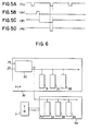
- the output circuit 15 generates a processing start timing signal PS from the frame start signal FL indicating the first line of each frame from the input circuit 14 and the processing end signal OK from the PVP 3B.
- the frame start signal FL is at a low level for a period of a clock at the start point of each frame (Fig. 5A).
- the frame start signal FL is delayed by a period of a clock in the delay circuit 17 and is then supplied to the clear terminal of the D-type flip-flop 18.
- the clock terminal of the flip-flop 18 is supplied with a signal OK from the PVP 3B to be set to a high level for a period of a clock 8 Fig. 5B).
- the D input of the flip-flop 18 is always at the high level.
- this flip-flop 18 is cleared by the frame start signal FL and hence the Q output DP thereof (Fig. 5C) is kept remained at the high level.
- the output DF is supplied to the OR gate 19.
- the OR gate 19 is in turn supplied with a frame start signal FL.
- the output from this OR gate 19 is the signal PS (Fig. 5D), and if the frame start signal FL is received when the output DF is at the low level, the output PS is set to the low level for a period in which the signal FL is at the low level.
- the signal OK is obtained for each frame end in any case, and hence the signal PS becomes identical with the frame start signal FL.
- the signal PS is different from the frame period and can be first obtained only in the next frame following an output of the signal OK.
- the entire data processing is automatically accomplished without necessitating the human intervention, namely, the frame next to the time of point when the preceding processing is finished is automatically fetched for the processing
- a manual switch is disposed for this purpose; and when the user specifies a frame to be processed, the signal PS is to be gated at the specified frame, that is, the signal PS is obtained only at the start point of the specified frame.
- the processing start timing signal is generated after a signal indicating the completion of a data processing is received from the data processing section, there does not occur an inconsistency that the next processing start signal is generated before the preceding processing is finished.
- the processing start timing need not be determined with a margin of rocessing time, and hence an effective data processing can be accomplished.
- the image data processing is effcted as described above.
- an image processor achieving the computer processing is used.
- a method for arranging a plurality of unit processors each having the same configuration and for simultaneously operating the processors at the same time is adopted as a method for processing the image data at a high speed.
- each processor in addition to a case where the plurality of processors can be controlled at the completely same operation tiding, there are cases where the different timing is required, namely, each processor must be started with a slight timing difference.
- a method for controlling the timing it is common to effect an independent timing control by independently sending a operation timing signal to each subsystem rather than to effect the timing control with a timing control system.
- the timing signal is shared among the plurality of subsystems.
- a timing control processor 30 is disposed as the main processor in the PVP 3B as described before.
- the processor 30 is supplied with the processing start signal PS from the IOC 1.
- the IOC 1 is in turn supplied with the processing end signal OK from the processor 30.
- the processor 30 sends as a timing signal TS a time series signal having a width of one bit to the other processors 31, 32, 33, etc. in the PVP 3B; furthermore, the timing signal TS is transmitted also to the processors 34, 35, 36, etc. of the PIP 3A.
- the 60 sheets of processors in the PIP 3A are controlled in groups each including ten sheets of processors.
- the processors 31, 32, 33, etc. and 34, 35, 36, etc. each are provided with a decoder for the timing signal TS.
- the decoder comprises a shift register 37, a bit pattern setting unit 38, and a comparator 39.
- the shift register 37 sequentially receives the timing signal TS from the control processor 30.
- the shift clock of the shift register 37 is synchronized with the transmission timing clock of the timing signal TS or is a clock having a frequency higher than the frequency of the transmission timing clock.
- the timing signal TS is transmitted in the bit-by-bit basis in response to the transmission timing clock, so that the signal is fetched into the shift register 37 such that, for example, a bit pattern of five bits are sequentially shitted bit by bit.
- a particular bit pattern specific to each processor is set to the pertinent bit pattern setting unit 38.
- the comparator 39 compares the 5-bit pattern of the timing signal TS stored in the shift register 37 with the 5-bit pattern in the setting unit 38. If the patterns match with each other, the operating timing signal TP of the processor to which this decoder is set is delivered from the comparator 39.
- the comparator Assuming now that, for example, a bit patter [1001] is contained in the setting unit 38, the comparator generates an operation timing signal TP at the timing when the bit pattern of the shift register 37 changing for each transmission clock becomes to be [1001].
- the timing control processor 30 saves the bit pattrn of the setting unit 38 of each decoder of the processors and performs and arithmetic processing, for example, to determine the transmission sequence of [0111] of the timing signal TS so as to supply a desired operation timing to each processor, and then the timing signal-TS is sent to the processors, thereby accomplishing the timing control of each processor.
- the bit pattern to be set by the bit,pattern setting unit 38 may contain data of which the number of bits is equal to or more than the number of bits of the shift register 37; furthermore, the number of bits may vary for each register.
- the processors 30 and 34 can be operated at the preceding timing of [101] and at the succeeding timing of [1001], respectively.
- the processors 33 can be operated at the preceding timing delayed by a transmission clock cycle with respect to the processor 32.
- each processor can perform a software processing to detect the bit pattern, thereby obtaining the operation timing.
- [1] may be transmitted in other than the transmission of the timing signal TS and [0] may be sent in the transmission of the timing signal TS, so that each processor counts the frequency of [1] to determine the operation timing.
- the frequency may be changed for each processor so as to determine the specific operation timing for each processor.
- the timing signal TS may be other than one bit wide, namely, the width may be of several bits; however, in such a case, the bit-parallel signal comprising a plurality of bits is required to be used as the timing signal, and hence a plurality of transmission lines are required. In a case of a 1-bit wide signal, only a transmission line is required.
- the timing signal is shared among a plurality of subsystems and the decode processing of the timing signal in each subsystem, namely, the algorithm for detecting the operation timing of each subsystem is changed, thereby enabling to supply the respective processing timing to the plurality of subsystems by use of a small-sized hardware.
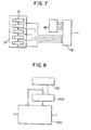
- the processors constituting the PIP 3A and the PVP 3B each comprises a control section provided with a microprogram stored therein for outputting a microinstruction and an arithmetic section for executing an arithmetic operation according to the microinstruction.
- the input digital data is supplied to the arithmetic section.
- a portion of the information of the arithmetic section is fed to the control section so as to reflect the arithmetic information to the program and the result of the arithmetic operation is obtained as an output digital data from the arithmetic section.
- the arithmetic section of the processor includes a multiplier, an adder/subtractor, and a factor memory for storing factors or coefficients necessary for the arithmetic operation such as for sing 0 and cos 0.
- Fig. 8 is a block diagram showing the overall configuration of an example of a processor for the digital operation to be used in the data processor according to the present invention.
- the microinstruction from the control section 100 is supplied to the main arithmetic section 300 and the auxiliary arithmetic section 200.
- the main arithmetic section 300 is supplied with an input data, which is then subjected to a signal value calculation, and then an output data is generated and is delivered.
- the auxiliary arithmetic section 200 generates addresses of the factor memory and the data memory disposed in the main arithmetic section 300 as will be described later and performs a computation for obtaining the value of repetition of the DO loop, and the addresses and the DO loop repetition value are delivered to the main arithmetic section 300 and the control section 100, respectively.
- Fig. 9 is a block diagram showing an example of the main arithmetic section 300 in which two systems of data operation units each for 8-bit operation are provide for the general-purpose processing, so that a 16-bit data operation is enabled in the system as a whole.
- the arithmetic units 300X and 300Y each have the completely same configuration, and hence the same reference numerals are assigned to the corresponding sections thereof together with suffix letters X and Y.
- the first arithmetic unit 300X comprises a multiplier 311X, an adder/subtractor 312X, a factor memory 313X, a data memory 314X, a plurality of registers 321X - 328X, and a tristate buffers 331X - 338X.
- the control section 100 sends microinstructions to determine whether or not the outputs from the registers 321X - 328X are to be enabled, whether or not the data is to be fetched, or whether or not the multiplier 311 is to be operated.
- the tristate buffers 331X - 338X are also controlled by the microinstructions.
- the input data is fed to the register 321X and the register 328X delivers an output data.
- the factor memory 313X contains the factor or coefficient data such as cos ⁇ and sin ⁇ .
- an address signal is supplied from the auxiliary arithmetic section 200 via the register 341XY to the factor memory 313X, a factor necessary for a signal value calculation is appropriately read therefrom.
- the data memory 314X is used to store the output data generated when necessary. when an address signal is supplied from the auxiliary arithmetic section 200 via the register 342XY to the data memory 314X, the data is read therefrom as appropriately.
- the second arithmetic unit 300Y is similarly configured in which the input data is supplied to the register 321Y and the register 328Y delivers an output data.
- An address from the auxiliary arithmetic section 200 is supplied via the register 341XY to the factor memory 313Y, whereas an address from the auxiliary arithmetic section 200 is fed via the register 342XY to the data memory 314Y.
- the first arithmetic unit 300X and the second arithmetic unit 301Y are so designed to process 16-bit data, namely, 32-bit data can be processed in the system as a whole.
- the system is configured to be capable of achieving a general-purpose processing so that the processing may be effected on either one of the first and second arithmetic units 300X and 300Y; moreover, the outputs from the adder/subtractor 312X and 312Y are supplied to the registers 323Y and 323X, respectively, whereas the outputs from the registers 327X and 327Y are delivered to the register 324 and the multiplier 311 and the register 324X and the multiplier 311X, respectively, thereby enabling information communication between the arithmetic sections 300X and 300Y.
- the adder/subtractor units 312X and 312Y are linked to each other by use of a joining section 350.
- a predetermined select signal is supplied to the joining section 350, the operation can be changed between two modes, namely, whether the respective adder/subtractor units 312X and 312Y each operate as a 16-bit adder/subtractor with the single precision or two adder/subtractor units 312X and 312Y operates as a unit to operate as a 32-bit adder/subtractor with the double precision.
- the adder/subtractor units 312X and 312Y each are constituted as a 16-bit adder/subtractor, for example, including four microprocessors Am2901 of AMD as a unit.
- the adder/subtractor for example, includes a RAM which is capable of storing 16 items of 16-bit data.
- the 16-bit data items are arranged so as to be shifted in the column direction according to the numeric relationships such as 1/2 time, 2 times, and so on.
- the TC 4 performs a comprehensive control in three modes to be described later, thereby enabling the processing execution, the processing termination, and the program transfer (exchange) without any inconsistency.
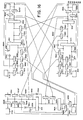
- Fig. 10 shows the connecting relationships between the TC and the control section 100 of one of the plural processors of the PIP 3A and the PVP 3B. This configuration applies to all the processors effecting the program exchange.
- the components other than the TC 4 constitute an example of the configuration of the control section of the processor.
- the microprogram controller 101 generates addresses of the microprogram memory 111 - 114a and 114b constituted from the RAM.
- microprogram memory 111 For example, four instruction bits are obtained to select one of a plurality of instructions of the microprogram controller 110, and the instruction bits are supplied via a register 115 to an instruction terminal I of the controller 110.
- the controller posseses 16 kinds of instructions.
- the selector 116 is supplied with a plurality of 1-bit information items, and one of these items is selected according to an information read from the microprogram memory 112.
- the 1-bit information from the selector 116 is supplied as a condition code to the terminal CC of the program controller 110 and is then combined with the instruction bits so as to be used as an information to select the next address as a data incremented, an address to be supplied to the direct input terminal D, or other address.
- An information for example, a destination address of a GO TO statement or an information of the repetition value of a DO loop is obtained from the microprogram memory 113 and is then latched into a register 117a.
- micro program memory 114a and 114b Form the micro program memory 114a and 114b, an information of the microinstruction is extracted. This information is supplied via the register 118 to the arithmetic section of this processor, and all or a part of the microinstruction is supplied to the add/subtract logic unit 201 as an auxiliary arithmetic section 200.
- the microprogram controller 110 is so designed to enable one of three enable signals PL, VECT, and MAP depending on the instruction bit. Consequently, one of the registers 117a - 117c is enabled by the instruction bit, and the address latched in the register is used as the direct input. In most instruction, the signal PL is enabled, namely, the signal VECT or MAP is enabled only for a particular instruction. Furthermore, whether the direct input is to be selected in the instruction bit state is determined according to the condition code from the selector 116.
- the add/subtract arithmetic unit 201 On receiving a microinstruction, the add/subtract arithmetic unit 201 obtains through calculation address signals of the factor memory 313X and 313Y and the data memory 314X and 314Y of the main arithmetic section 300 and supplies the obtained address signals to the registers 341XY and 342XY for the storage.
- an information such as the repetition value of a DO loop is obtained through a computation and is fed, for example, to the register 117b.for the storage.
- auxiliary arithmetic section 200 Operations in the auxiliary arithmetic section 200 are relatively simpler than the signal value calculation of the main arithmetic section 300; consequently, as the example described above, the auxiliary arithmetic section 200 can be of a small size as hardware like the add/subtract arithmetic unit 201.
- auxiliary arithmetic unit 200 when the auxiliary arithmetic unit 200 is provided, for example, in a case where a computation of the total of operations between the coefficients KA(a l ), KA(a 2 ), ... KA(an) at the addresses a 1 , a 2 , ... an of the factor memory 313X and the data TA(a l ), TA(a 2 ), ...
- TA(a n ) at the respective addresses of a 1 , a 2 , ⁇ an of the data memory 314X namely, KA(a 1 ) * TA(a 1 ) + KA(a 2 ) * TA(a 2 ) + ⁇ + KA(a n ) * TA(a n ) and a computation of the total of operations between the coefficients KB(a 1 ), KB(a 2 ), ⁇ KB(a n ) at the addresses a 1 , a 2 , ⁇ a n of the factor memory 313Y and the data TB(a 1 ), TB(a 2 ), ⁇ TB(an) at the respective addresses of a 1 , a 2 , ...
- the processing can be accomplished in n steps or slightly greater than n steps as compared with 2n steps required in the prior art technique, which enables to improve the processing speed.
- the auxiliary arithmetic section is provided to calculate values such as the memory address of the factor memory of the main arithmetic section performing the signal value calculation, the operations such as the address value calculation conventionally achieved in the main arithmetic section are relieved therefrom, and hence the main arithmetic section effects only the signal value calculation, thereby increasing the execution speed of the processing.
- the selector 116 is supplied as an input information the information from the arithmetic section and the information from other processor, and depending on the information, an instruction, for example, a conditional jump is effected.
- the memory units 114a and 114b are provided as the microprogram memory for supplying microinstructions to the first data system.
- the outputs from the memory 114a and 114b are connected (wired ORed) with each other and are linked via the register 118 to the first data system.
- the information from the first data system is supplied as the chip select signal CS 1 to the memory 114a and is delivered via an inverter 122 to the memory 114b.
- the contents of the microprogram memory 114a and 114b in a case where a computation of C A +
- is achieved will be as follows.
- an adaptive processing such as a calculation of an absolute value can be conducted.
- the address capacity of the program memory is greater than the program length, it is possible to dispose two memory such as the memory 114a and 114b of the example described above. These memory units are not selected through a chip select operation, namely, two kinds of program contents are written in a memory device, thereby enabling to select one of these two kinds of programs by supplying the information from the data system to the MSB of the address.
- the adaptive processing associated with the information from the data system can be simply achieved without changing the program flow.
- the TC 4 comprises an RAM 41 for storing programs to be supplied to the microprogram memory 111 - 114a and 114b and an address generator 42 for generating the addresses thereof.
- the mode signal generate means 43 is disposed to generate 1-bit mode signals MA and MB; furthermore, there is provided the write signal generate means 44 for generating a program write signal for the microprogram memory 111 - 114a and 114b in the program exchange mode.
- the mode signal generate means 43 is configured, for example, as shown in Fig. 11.
- switches SWA and SWB are to be changed over by the operator.
- Each switch has an input A applied with a positive direct current (dc) voltage and other terminal B grounded.
- a signal a to be obtained by the switch SWA is supplied to an input terminal of an OR gate 45.
- a signal b obtained by the switch SWB is delivered as a mode signal MB and is supplied to other input terminal of the OR gate 45, which in turn delivers a mode signal MA.
- the mode is set as follows depending on the 1-bit mode signals MA and MB.
- the execution mode is set regardless of the state of the switch SWA. If the switch SWA is set to the terminal A and the switch SWB is set to the terminal B, the reset mode is set. If the switch SWB is set to the terminal B and the switch SWA is set to the terminal B, the program exchange mode is set.
- this mode signal MB is signified as a reset (halt) signal.
- the selector 120 selects addresses for the microprogram memory 111 - 114a and 114b from the addresses from the program controller 110 and the TC 4.
- the signal MA is supplied.
- the signal MA is 1, the address from the microprogram controller 110 is selected, and when this MA is 0, the address from the TC 4 is selected.
- the gate circuit 121 gates the write signal WR according to the gate signal MA.
- the gate signal M A is 0, the gate is opened and the signal WR is supplied to each write enable terminal WE of the microprogram memory 111 - 114a and 114b.
- the microprogram memory are set to the write enable state.
- the signal MB is fed to the reset terminal of the register 115, and when this signal MB is 0, the register 115 is reset.
- the states of the mode signals.MA and MB are monitored by the load control section 46 so as to control the processing in the TC 4 according to the mode.
- the mode signal MA is 1, and hence an address from the microprogram controller 110 is obtained from the selector 120, and this address signal is subjected to a delay of a clock via the register 119 and the resultant signal is supplied to the microprogram memory 111 - 114a and 114b.
- the output from the OR gate 121 is 1 in any case when the signal MA is 1, and the memory 111 - 114a and 114b are therefore not set to the write enable state.
- the register 115 is not reset and the data read from the microprogram memory 111 is subjected to a delay of a clock in the register 115 and is supplied to the instructibn terminal of the microprogram controller 110, thereby executing a program.
- the microinstruction read from the microprogram memory 114 is delayed by a clock in the register 118 and is supplied to the arithmetic section.
- the pipeline registers are designed to be disposed as follows.
- a register 119 is located between the program controller 110 and the microprogram memory 111 - 114a and 114b, the registers 115 and 117a are disposed between the output sides of the microprogram memory 111 - 114a and 114b and the program controller 110, and a register (not shown) is connected to the input of the selector 116. This provision enables to decrease the clock cycle.
- the parallel processing method by use of the multiprocessor configuration is primarily adopted, however, the pipeline processing method as described above is also partly utilized to effect a high-speed processing.
- the mode signal MB is 0, and hence the register 115 is reset and [0000] is supplied to the instruction terminal of the program controller 110; consequently, the address supplied from this program controller 110 is kept to be 0 or the address output is stopped. Namely, the program addresses for all processors associated with the PIP 3A and PVP 3B are 0 and hence the program stop state is set.
- the selector 120 is set to the state to select the address from the address generator 42 of the TC 4.
- the microprogram memory of all processors is under control of the TC 4.
- the signal MA may be fed to the output enable terminal OE of the program controller 110 so as to set the output buffer of the program controller 110 to off.
- an instruction from the load control section 46 causes the address generator 42 to send an address to the R AM 41, and the program data to be transmitted to the microprogram memory 111 - 114a and 114b is read from the RAM 41.
- the write signal WR from the write signal generate means 44 is set to 0 and the mode signal MA is 0; consequently, the output from the OR gate 121 is also set to 0, which sets the microprogram memory 111 - 114a and 114b to the write enable state.
- the program data from the RAM 41 is sequentially written in the microprogram memory 111 - 114a and 114b according to the address from the address generate means 42, thereby achieving the program transfer.
- the program transfer is sequentially accomplished for each processor.
- the TC 4 is provided with the ROM 47 in which the processor select signal is stored.
- the processor select signal is read according to an instruction from the load control section 46.
- the processor select signal is decoded in the decoder 48 and only the select signal SEL for the processor to be selected is set to 0 and the other signals are set to 1.
- the select signal SEL is kept supplied to the OR gate 121, and only the microprogram memory 111 - 114a and 114b of the processor for which the select signal SEL is 0 is set to the write enable state, and then a program rewrite operation is effected.
- the execution start address is extracted from the RAM 49 and is supplied to the register 117c of each processor.
- the select signal SEL is delivered as a latch signal of the register 117c, and at a timing when the select signal changes from 0 to 1, the execution start address is latched.
- the register 117c is enabled by the enable signal MAP from the microprogram controller 110, and the latched data is supplied to the direct input terminal D.
- the address from this register above when a program starts, the address from this register 117c is fetched into the program controller 110, which in turn generate the addresses beginning from the fetched address.
- the execution start address for each processor stored in the RAM 49 is supplied from the host computer 5 in advance.
- the microprogram controller 110 continues sending address 0 or is in the stop state.
- a start address of a program to be executed is reassigned. That is, like in the program transfer operation, the processor select signals are sequentially outputted from the ROM 47 and the execution start address is sequentially supplied from the RAM 49 to each processor, and then the execution start address is sequentially latched into the register 117c of each processor according to the signal SEL.
- each processor executes the program beginning from the reassigned execution start address. Namely, without transferring the new program, another program can be executed in each processor.
- the three modes described above are controlled by a program of the processor in the TC 4.
- the data processing section 3 reads for processing the necessary items from the image data stored in the VIM 2 and writes the processed data again in the VIM 2. Consequently, for a group of image data, such as a field or frame of image data, in addition to a case where all pixel data items are read for the work thereof, there is a case where only the necessary image data is read from a plurality of fields, a plurality of fields obtained from a frame memory, or data astriding a plurality of frames, and the obtained data is subjected to the work processing to generate a field or'frame of data, which is then written in a field or a frame memory.
- the control of data internal with respect to the VIM 2 is effected mainly by the address generate section in the VIM 3.
- the address generation section a processor is utilized, and the processor operates to generate through a calculation addresses for various kinds of processing.
- the characteristic required for the address generation varies depending on the processing kind. Namely, the addresses required for the processing are mainly classified into two types as follows.
- the address generate section of the PVP 3B includes a first processor 301 for generating through a computation a simple address and a second processor 302 for generating through a calculation a complicated address as shown in Fig. 12.
- reference numeral 303 indicates an address generation control processor for controlling the first and second processors 301 and 302.
- Reference numeral 304 denotes a selector which selects from three address data including the address data from the first and second processors 301 and 302 and a compound address data obtained by executing a computation in the arithmetic circuit 305 on the address data from the first and second processors one address data according to a select signal from the address generation control processor 303.
- the first processor 301 generates an address for sepcifying, for example, a rectangular area on a screen and can be implemented by use of counters for this purpose.
- the rectangle addresses can be generated in the horizontal and vertical directions.
- the second processor 302 is, for example, a general-purpose processor which operates according to a microprogram, and in addition to the linear operation, this processor can achieve the nonlinear operation and an adaptive operation and the program is supplied thereto from the TC 4.
- the address generate control processor 303 supplies control signals such as a start signal and parameters to the first processor 301.
- the second processor 302 is supplied with control signals such as a program start signal, whereas the parameters and other information are delivered from the TC 4.
- microprogram is fed from the TC 4 to the address generation control processor 303.
- the address generation control processor 303 for example, the sum of the addresses from the first and second processors 301 and 302 is calculated.
- the second processor 302 obtains through a computation the position P of the uppr-left corner of the rectangular area, and the address data of the position is kept delivered from the second processor 302 so as to be supplied to the arithmetic circuit 305.
- the address generation control processor 303 delivers to the first processor 301 a parameter indicating the size of the rectangular area.
- the first processor 301 then generates the rectangle addresses ranging from the point Po of the upper-left corner of the screen A to the portion enclosed with the broken lines.
- the addresses are obtained for the objective area indicated with the shade in Fig. 13.
- the selector 304 selects an address from the arithmetic circuit 305 based on the select signal from the control processor 303.
- the address generation for the area indicated with the shade in Fig. 13 is to be accomplished by a processor,f a calculation to obtain the point P 1 and a calculation to regularly generate the addresses of the rectangular portion are required, and the processing speed is lowered; however, like in this example, the second processor 302 keeps outputting the address of the point P 1 and the first processor 301 regularly delivers an address at a high speed so that an addition is conducted in the arithmetic circuit 305, thereby enabling to generate a regular address at a high speed beginning from the address calculated by the second processor 302.
- the first processor can generate any regular data, for example, an address having the inversed bit order necessary for an operation of the Fast Fourier Transformation (FTT) is generated by the first processor 301.
- FTT Fast Fourier Transformation
- the selector 304 selects one of the addresses from the first and second processors 301 and 302
- one of the following methods can be adopted, namely, the first method in which the selection is effected according to the address generation speed, the second method in which the selection is achieved according to the processing speed in the PIP 3A executing the arithmetic processing on the pixel data, or the third method in which the selection is conducted according to the total of the processing time for the address generation and for the processing in the PIP 3A.
- the selector 304 is so designed to receive an address with the high speed.
- the system selects an address having the less probability of errors even if the processing speed is low.
- the addresses matched for the processing can be effectively generated.
- a plurality of processors are provided to generate a plurality of addresses, respectively, and in addition to the selection of the generated addresses by use of a selector, the plural addresses thus generated are appropriately computed by another arithmetic circuit and are combined to generate another address; consequently, the processing capacity is increased in the processing system.
- the configuration need only includes a simple arithmetic section and a control section; however, if the PIP 3A is to achieve a generation of a complicated address, a simple configuration of the PVP 3B cannot sufficiently cope with the condition.
- the PVP 3B is provided with a PVPP section 361 as a first processing section and information such as a frame start signal is communicated between the PVPP 361 and the IOC 1.
- a simple address such as an address of a rectangular area is generated according to a microprogram, and the signals such as a control signal and a timing signal for the other processing section are also generated, thereby controlling the entire operation of the PVP 3B.
- the addresses of the rectnagular area can be generated in the longitudinal and vertical directions and in the inversed bit sequence.
- the control signal from the PVPP 361 is supplied to the PVPCF 362 as the second processing section.
- an input/output control signal for the PIP 3A is generated depending on the control signal from the PVPP 361 according to the microprogram and is delivered to the PIP 3A.
- control signal from the PVPP 361 is supplied to the PVPCA's 363A and 363B as the third processing sections.
- Two systems of PVPCA's 363A and 363B are provided for the VIM's 2A and 2B; in addition, the PVPCA's include nine circuits Il - I9 and 01 - 09, respectively as the processor sections which are equivalent to the processor section of the PIP 2A.
- addresses having a nonlinear change or an adaptive change are generated according to the respective microprograms.
- control signal from the PVPP 361 is supplied to the processing control section (CAT) 364, which in turn sends a signal to control the input/output of each processor of the PVPCA's 363A and 363B. Addresses from the processors of the PVPCA's 363A and 363B are fed to the DOG's 365A and 365B.
- CAT processing control section
- the DOG's 365A and 365B are configured, for example, as shown in fig. 15.
- a 3-dimensions constituted from 16 bits for each of X, Y and Z is fed from the PVPCA 363A to the input register 367.
- the addresses associated with the 19 bits of the X and Y coordinates are outputted to the PVPCNT 366 to be described later.
- a 48-bit address is delivered from the register 367 to the address register 368 and is subjected to a predetermined timing matching and other processing; and then the resultant signal is supplied to the PVPCA 363A or the other DOG 365B through the first input of the multiplexer (MUX) 369.
- MUX multiplexer
- a 48-bit address from the DOG 365B is fed via the register 370 to the second input of the MUX 369. Moreover, the 19 bits address of the x-y coordinate from the register 37 and the eight bits of the z-coordinate address are delivered to the register 37a. The 19 bits thereof are transferred for an address of the memory 372 and the eight bits thereof are supplied for the data of the memory 372. This causes an 8-bit data associated with the z-coordinate to be stored in the memory 372 according to the x-y address.
- a 32-bit address of x-y coordinate is supplied from the register 367 to the register 373, and then the 32-bit address is fed to the third inpur of the MUX 369 together with the eight bits read from the memory 372 and additional eight bits, for example, comprising 0, namely, a total of 48 bits are'delivered as an address.
- a 4-bit control signal from the CAT 364 is fed to the register 374 and is used to control the timing of the register 368, the selection on the three inputs of the MUX 369, and the write operation on the memory 372.
- the addresses from the processors of the PVPCA's 363A and 363B are delivered and are further retransmitted to the PVPCA's 363A and 363B for complicated processing; furthermore, a communication is conducted with the other DOG to relate the addresses on the input and output sides to each other.
- the z-coordinate address data may be stored to be corresponded to the 3- dimensional information and the pixel index.
- the addresses from the DOG's 365A and 365B and the address generated by the PVPP 361 are transmitted to the select circuit PVPCNT 366, which in turn supplies the addresses to the MUX 366A and the MUX 366B.
- These MUX's 366A and 366B are controlled by the PVPP 361 to obtain the addresses from the DOG or PVPP or to generate an address by adding the addresses.
- the resultant addresses are delivered to the VIM's 2A and 2B.
- the address generation is conducted as described above. According to this system, since the functions necessary to generate addresses and control signals are efficiently subdivided, the loads on the respective processing sections can be reduced and the processing including the complex operations can be quite simply accomplished.
- Fig. 16 is a schematic circuit diagram showing the connection of the PVP 3B to calculate a 3- dimensional address in which the address generate section 300 is provided with an address generate section 30DZ for generating a z-directional address in addition to the configuration of Fig. 9.
- the address generate section 30DX, 30DY, and 30DZ each are provided with the registers 326X', 329X, 329X', and 330X in addition to the configuration of Fig. 9.
- the address generate sections 30DX, 30DY, and 30DZ of the three directions areconnected to each other, so that for an address generation in each direction, the results of the address generations in the other directions can be appropriately used.
- the outputs from the adder/subtractor units 312X, 312Y, and 312Z are supplied to registers so that one of the outputs related to a direction is supplied to the multiplier 311X of the address generate sections for the other two directions, and the outputs from the adder/subtractor units 312X, 312Y, and 312Z are temporarily stored in registers and then are further supplied to registers, so that the outputs are inputted to an adder/subtractor of the address generate sections related to the other two directions.
- the image to be inputted is represented with the address information in the X and Y directions
- the 3- dimensional, positional information of the original object to be displayed as an image namely, the depth information is stored in the Z memory (not shown).
- a parallelopiped in the 3-dimensional space is rotated by 0 about a line A parallel to the y axis.
- an arbitrary point (Xl, Y l , Z l ) on the parallelpiped is moved to a position (Xi, Yi, Zi).
- the values of X, Y, and Z can be obtained as follows.
- Fig. 18A is a flowchart of a program executed in the first address generate section
- Fig. 18B is a flowchart of a program executed in the PIP 3A
- Fig. 18C is a flowchart of a program executed in the second address generate section.
- the addresses of the X and Y directions are supplied to the VIMIN 2A beginning from "0", and the input image data for a screen is entirely read and is inputted to the P I P 3A.
- the image data supplied to the PIP 3A is delivered to the VIMOUT 2B.
- the obtained addresses of the Z direction are supplied as inputs to the arithmetic and generate section 300Z for the Z direction.
- the second address On receiving the address information of the three directions, the second address generate section conducts the calculation (a) described above.
- the address (X i , Y i ) in the two directions Xi and Yi are used to write.the data of (X 1 , Y 1 ) in the VIMOUT 2B.
- the addresses of the VIMIN 2A and the VIMOUT 2B are read and written with respect to the same two directions, an image of an object viewed from another direction can be easily obtained by changing the directions of the 2-dimensional addresses such that the addresses of the memory 2A are read and written in the X and Y directions and the addresses of the memory 2B are manipulated in the X and Z directions.
- contour extraction is an example of the neighborhood processing.
- the methods for processing the contour extraction includes a method using a logic filter, which will be described herebelow.
- each pixel data comprising eight bits is represented in the binary form, and the obtained data is subjected to an operation by use of a 3 x 3 logic filter, thereby extracting a contour of an image.
- the logical sum of the nine binary pixels is then obtained as follows.
- the binary central value b is subtracted from the logical sum values A, B, and C as follows.
- the result of this operation is outputted as a value of the central value b 2 of the ine pixels.
- the processing for each pixel is effected through the overall screen to achieve the contour extraction.
- the logical sum of pixel data in the binary form comprising 0 or 1 is generated.
- the region 401 indicated with the shade originally having the value 1 in the binary representation is slightly enlarged (by about one pixel), and the original region 401 of the value 1 is removed from the enlarged region, so that there remains the portion 402 indicated with the shade in Fig. 8.
- This region comprises the pixels enclosing the region the value of which has become to be 1 through the enlarging operation, thereby obtaining the contour.
- the methods of the binary conversion include the P tile method, the mode method, the defferential histogram method, and the discrimination analysis method.
- the binary conversion in this system is conducted by use of the threshold value determined according to one of these method.
- the delay circuits 403 and 404 each for delaying a period of a horizontal scanning are used to simultaneously extract for the current data DA the data DL l advanced with respect thereto by a horizontal scanning period and the data DL2 delayed with respect thereto by a horizontal scanning period, so that the data of three pixels to be vertically arranged on the screen is to be processed at the same time.
- the data for the nine pixels is fetched, for example, into the register section disposed as an input stage of the processor, thereby accomplishing the processing.
- the data processing is delayed for the delay time related to the delay circuits, which disables the realtime processing.
- the realtime processing is executed in this case, the following problem arises. That is, in a case of the neighborhood processing using a 3 x 3 logic filter as described above, for example, the data of nine pixels is necessary to obtain an output associated with a pixel. Consequently, the data transfer rate on the input side must be nine times the data transfer rate on the output side.
- the realtime processing cannot be accomplished only by inputting the data to the processor.
- the overall screen data is split into blocks B each including 20 horizontal lines as shown in Fig. 22, and 20 processors are disposed so that the neighborhood processing of a line of each block B is executed by one of the processors.
- a processor calculates the result of a line by use of data related to three lines.
- the input data to the processor for processing the data is read from the input image memory; however, in this example, the equal data transfer rates can be implemented on the input and output sides by appropriately setting the sequence for reading the pixels from the input image memory, by simultaneously transferring the pixel data to the processor requiring the data, and by using the register disposed in the input stage of each processor.
- F ig. 23 is a diagram showing a block including 20 lines of the input image memory in which lines L l , L 2 , ... L 20 correspond to processors P 1 , P 2 , ... P 20 , respectively.
- the pixel data is read from the input image memory in the sequence, namely, in the vertical direction as marked by an arrow mark 405.
- the 20 pixels arranged in the vertical direction are read from the block and are consecutively transferred to the processor side.
- the transfer data is simultaneously fetched into the.input register of the processor requiring the data.
- the pixel data d (1, 11) of the eleventh position of the line L l is transferred to the processors P 1 and P 2
- the pixel data d (2, 11) of the eleventh position of line L 2 is delivered to the processors P l , P 2 , and P 3
- the pixel d .(3, 11) of the eleventh position of the line L 3 is delivered to the processors P 2 , P 3 , and P 4
- the pixel d (4, 11) of the eleventh position of the line L 4 is transmitted to the processors P 3 , P 4 , and P 5 , and so on.
- the data is sent to the processors P 1 - P 20 through the input registers, respectively.
- the data stored in the input registers of the processors P 1 - P 20 is combined with the ninth and tenth pixel data d (i, 9) and d (i, 10) in the lines L l - L 20 so as to be processed as the data of the nine pixels necessary for calculating the output values of the tenth central pixel.
- the data of six pixels among the data of nine pixels is also used as the pixel data to calculate the output value of the preceding ninth central pixel data.
- buffer registers 421 - 425 are' included as the first stage.
- the input terminal for the input pixel data is configured to be commonly supplied to the buffer registers, and the timing to supply clocks to the registers are controlled, thereby fetching the necessary pixel data in the pertinent registers.
- the system achieves an operation so that the pixel data is simultaneously transferred from these registers to the shift registers 411 - 413 for the first, second, and third lines.
- the pixel data of the nine pixels is transferred to the arithmetic section of the processor so as to effect the contour extract processing described above.
- the transfer of the data from the shift registers 411 - 413 to the arithmetic section of the processor is accomplished by use of instructions of a processing program stored in the control section of the processor.
- the processing associated with the pixel data of the nine pixels is to be completed by the time when the pixel data of nine pixels for the next data in the line to be processed by the processor is fetched.
- the eleventh pixel data d (2, 11) in the line L 2 is fetched into the buffer register 423 for the third line in the input register of the processor P1, the buffer register 422 for the second line in the input register of the processor P 2 , and the buffer register 421 for the first line in the input register of the processor P 3 at the same time.
- the eleventh pixel data d (3, 11) in the line L 3 is fetched into the buffer register 423 for the third line in the processor P 2 , the buffer register 422 for the second line in the processor P 3 , and the buffer register 421 for the first line in the processor P 4 at the same time.
- each processor naturally posseses a processing speed which allows the contour extract processing to be completed by the time when the data each including three pixel data is transferred to the next stage in the shift registers 411 - 413:
- the first and last lines of the 20 lines cannot be appropriately processed. (This is because the preceding line is missing for the first line and the succeeding line is missing for the last line).
- the block division if an overlap of at least one line is provided for each block as shown in Fig. 26, the number of lines for which the appropriate processing is effected can be reduced.
- the input register section need not be necessarily disposed in the processor, namely, the same operation can be achieved even if the input register section is located as the preceding stage of the input of the processor.
- a plurality of processors are utilized and the data is simultaneously transferred to the processors requiring the data, which enables the same data transfer rate to be implemented on the input and output sides and hence to accomplish a realtime processing.
- the address is to be represented by use of ten bits and hence the configuration of the address generation and supply operation must be implemented for a total of 20 bits for two units of the factor memory. Consequently, the configuration of the address generate section in the control section 100 becomes complex and to be of a great size; furthermore, it is not easy to dispose two lines for supplying the address information.
- two input registers are supplied with a data select signal from the control section 100, and the selected data is fed to the input registers of the multipliers 311X and 311Y constituting the arithmetic sections 300X and 300Y, respectively.
- the factor memory units 313X and 313Y are supplied with the address read from the control section 100, and the factor thus read is delivered to the multipliers 311X and 311Y, which are then driven according to a control signal from the control section 100 and the operation results are fed to the adder/subtractor units 312X and 312Y, respectively.
- the data from the output reigsters of these adder/subtractor units 312X and 312Y is fed back thereto, and the adder/subtractor units are driven by the control signal from the control section 100 to deliver the operation result, which is in turn written in the output registers 328X and 328Y, respectively.
- the data from the output registers 328X and 328Y is fed to the output port according to the control signal from the control section 100.
- Xij indicates a data item
- Yij is an operation result.
- x i-1 , j-1 is read from FRA and is transmitted to the multiplier 311X.
- a 13 is read from the factor memory 313Y and is fed to the multiplier 311Y.
- X i+1 , j+j is read from the input register 321X and is delivered to the multiplier 311Y.
- the 3 x 3 spatial filter is implemented as described above.
- the factors all and a 13 of the step j, the factors a 21 and a 23 of the step j+l, and the factors a 31 and a 33 of the step j+3 are obtained from the factor memory units 313X and 313Y, which is required at the same point of time.
- these factors are written at the pertinent addresses of the respective memory units 313X and 313Y, so that address 0, address 1, address 2, address 3, and address 4 are read in the steps, j, j+l, j+2, j+3, and j+4, respectively, thereby extracting these factors in the similar fashion to the ordinary manner.
- the system described above is more effective as the number of the memory units is increased. For example, if the number is n, the number of the address generating sections as well as the signal supply lines can be reduced to 1/n time that required in the conventional system.
- each factor memory can be read by u,se of the common address, the read address generation in the control section is facilitated; furthermore, the number of the signal supply lines is reduced, which enables to simplify the configuration of the system.
Applications Claiming Priority (4)
| Application Number | Priority Date | Filing Date | Title |
|---|---|---|---|
| JP254528/85 | 1985-11-13 | ||
| JP25452885A JPS62114044A (ja) | 1985-11-13 | 1985-11-13 | アドレス発生装置 |
| JP259539/85 | 1985-11-19 | ||
| JP60259539A JP2610817B2 (ja) | 1985-11-19 | 1985-11-19 | アドレス生成装置 |
Publications (3)
| Publication Number | Publication Date |
|---|---|
| EP0222405A2 true EP0222405A2 (fr) | 1987-05-20 |
| EP0222405A3 EP0222405A3 (en) | 1989-08-23 |
| EP0222405B1 EP0222405B1 (fr) | 1994-09-14 |
Family
ID=26541714
Family Applications (1)
| Application Number | Title | Priority Date | Filing Date |
|---|---|---|---|
| EP19860115803 Expired - Lifetime EP0222405B1 (fr) | 1985-11-13 | 1986-11-13 | Processeur de données |
Country Status (6)
| Country | Link |
|---|---|
| EP (1) | EP0222405B1 (fr) |
| CA (2) | CA1283738C (fr) |
| DE (1) | DE3650069T2 (fr) |
| FR (2) | FR2593622B1 (fr) |
| GB (3) | GB2183067B (fr) |
| NL (1) | NL8602885A (fr) |
Cited By (3)
| Publication number | Priority date | Publication date | Assignee | Title |
|---|---|---|---|---|
| EP0325310A1 (fr) * | 1988-01-11 | 1989-07-26 | Koninklijke Philips Electronics N.V. | Système de traitement vidéo ainsi que système de reproduction d'images et de mémorisation d'images muni d'un tel système de traitement vidéo |
| US5434972A (en) * | 1991-01-11 | 1995-07-18 | Gec-Marconi Limited | Network for determining route through nodes by directing searching path signal arriving at one port of node to another port receiving free path signal |
| EP1555828A1 (fr) * | 2004-01-14 | 2005-07-20 | Sony International (Europe) GmbH | Procédé de prétraitement de données vidéo en blocks |
Families Citing this family (2)
| Publication number | Priority date | Publication date | Assignee | Title |
|---|---|---|---|---|
| GB2229336B (en) * | 1989-03-17 | 1993-09-15 | Sony Corp | Picture manipulation |
| US5237657A (en) * | 1989-03-17 | 1993-08-17 | Sony Corporation | Apparatus for manipulating a picture represented by a video signal |
Citations (4)
| Publication number | Priority date | Publication date | Assignee | Title |
|---|---|---|---|---|
| US4290133A (en) | 1977-10-25 | 1981-09-15 | Digital Equipment Corporation | System timing means for data processing system |
| JPS58215813A (ja) | 1982-06-09 | 1983-12-15 | Sony Corp | デイジタル信号処理装置 |
| GB2137847A (en) | 1983-03-28 | 1984-10-10 | Dainippon Screen Mfg | Picture Image Processing System |
| EP0150910A2 (fr) | 1984-01-04 | 1985-08-07 | Itek Corporation | Processeur digital de trame d'image |
Family Cites Families (48)
| Publication number | Priority date | Publication date | Assignee | Title |
|---|---|---|---|---|
| NO119615B (fr) * | 1966-02-25 | 1970-06-08 | Ericsson Telefon Ab L M | |
| FR2028240A1 (fr) * | 1969-01-13 | 1970-10-09 | California Computer Products | |
| NL7110608A (fr) * | 1970-10-05 | 1972-04-07 | ||
| US4330822A (en) * | 1971-09-02 | 1982-05-18 | Burroughs Corporation | Recursive system and method for binding compiled routines |
| FR2296221A1 (fr) * | 1974-12-27 | 1976-07-23 | Ibm France | Systeme de traitement du signal |
| US4024510A (en) * | 1975-08-28 | 1977-05-17 | International Business Machines Corporation | Function multiplexer |
| GB2017987B (en) * | 1978-03-29 | 1982-06-30 | British Broadcasting Corp | Method of and apparatus for processing data particularly digital audio signals |
| DE2963153D1 (en) * | 1978-06-26 | 1982-08-12 | Environmental Res Inst | Apparatus and method for generating a transformation of a first data matrix to form a second data matrix |
| US4244019A (en) * | 1978-06-29 | 1981-01-06 | Amdahl Corporation | Data processing system including a program-executing secondary system controlling a program-executing primary system |
| GB2052813B (en) * | 1979-05-31 | 1983-03-09 | Micronology Ltd | Interface unit between a computer and a hardcopy output device |
| US4363104A (en) * | 1980-09-22 | 1982-12-07 | Hughes Aircraft Company | Imaging system having multiple image copying and hierarchical busing |
| JPS5790650A (en) * | 1980-11-28 | 1982-06-05 | Toshiba Corp | Control device for copying machine |
| US4510568A (en) * | 1981-05-25 | 1985-04-09 | Fanuc Ltd. | Graphic processing method |
| US4503490A (en) * | 1981-06-10 | 1985-03-05 | At&T Bell Laboratories | Distributed timing system |
| JPS58139241A (ja) * | 1982-02-10 | 1983-08-18 | Toshiba Corp | 画像メモリアクセス方式 |
| US4542453A (en) * | 1982-02-19 | 1985-09-17 | Texas Instruments Incorporated | Program patching in microcomputer |
| GB2119594B (en) * | 1982-03-19 | 1986-07-30 | Quantel Ltd | Video processing systems |
| US4530051A (en) * | 1982-09-10 | 1985-07-16 | At&T Bell Laboratories | Program process execution in a distributed multiprocessor system |
| JPS5979349A (ja) * | 1982-10-29 | 1984-05-08 | Toshiba Corp | 演算装置 |
| DE3241189A1 (de) * | 1982-11-08 | 1984-05-10 | Siemens AG, 1000 Berlin und 8000 München | Taktstromversorgung fuer ein multimikrocomputersystem in eisenbahnsicherungsanlagen |
| US4590556A (en) * | 1983-01-17 | 1986-05-20 | Tandy Corporation | Co-processor combination |
| GB2138182B (en) * | 1983-04-14 | 1986-09-24 | Standard Telephones Cables Ltd | Digital processor |
| JPS59198513A (ja) * | 1983-04-26 | 1984-11-10 | Nec Corp | デイジタル信号処理装置 |
| EP0153439B1 (fr) * | 1983-06-03 | 1993-08-04 | Fondazione Pro Juventute Don Carlo Gnocchi | Système modulaire expansible pour traitement en temps réel d'un affichage TV, utile en particulier pour l'acquisition de coordonnées d'objets de forme connue et méthode utilisant cedit système en radiographie. |
| US4514647A (en) * | 1983-08-01 | 1985-04-30 | At&T Bell Laboratories | Chipset synchronization arrangement |
| FR2569071B1 (fr) * | 1983-09-30 | 1988-10-14 | Thomson Csf | Dispositif de traitement numerique de signal |
| US4646075A (en) * | 1983-11-03 | 1987-02-24 | Robert Bosch Corporation | System and method for a data processing pipeline |
| US4586038A (en) * | 1983-12-12 | 1986-04-29 | General Electric Company | True-perspective texture/shading processor |
| US4680628A (en) * | 1984-01-04 | 1987-07-14 | Itek Corporation | Realtime digital diagnostic image processing system |
| JPS60151789A (ja) * | 1984-01-19 | 1985-08-09 | Hitachi Ltd | 多機能画像処理プロセツサ |
| AU576348B2 (en) * | 1984-02-29 | 1988-08-25 | Measurex Corporation | Processing information |
| US4751637A (en) * | 1984-03-28 | 1988-06-14 | Daisy Systems Corporation | Digital computer for implementing event driven simulation algorithm |
| GB2161666A (en) * | 1984-07-09 | 1986-01-15 | Philips Electronic Associated | Video signal processing arrangement |
| GB2158321B (en) * | 1984-04-26 | 1987-08-05 | Philips Electronic Associated | Arrangement for rotating television pictures |
| JPS60231235A (ja) * | 1984-04-27 | 1985-11-16 | インタ−ナショナル ビジネス マシ−ンズ コ−ポレ−ション | イメ−ジ処理システム |
| GB8419291D0 (en) * | 1984-07-27 | 1984-08-30 | Micro Consultants Ltd | Image processing apparatus |
| DE3580552D1 (de) * | 1984-08-02 | 1990-12-20 | Telemecanique Electrique | Programmierbare steuereinrichtung mit zusatzprozessor. |
| NO843822L (no) * | 1984-09-24 | 1986-07-08 | Olav Holberg | Regnemaskinstruktur for ekstrapolasjon av boelgefelt. |
| GB8428443D0 (en) * | 1984-11-10 | 1984-12-19 | Int Computers Ltd | Data processing |
| US4742443A (en) * | 1985-03-28 | 1988-05-03 | Allen-Bradley Company | Programmable controller with function chart interpreter |
| GB2174860B (en) * | 1985-05-08 | 1989-06-28 | Sony Corp | Methods of and circuits for video signal processing |
| DE3579924D1 (de) * | 1985-05-20 | 1990-10-31 | Howard D Shekels | Superrechnersystemarchitektur. |
| GB2177871B (en) * | 1985-07-09 | 1989-02-08 | Sony Corp | Methods of and circuits for video signal processing |
| JPH0632053B2 (ja) * | 1985-07-17 | 1994-04-27 | シャープ株式会社 | 集積回路装置 |
| JPS6247786A (ja) * | 1985-08-27 | 1987-03-02 | Hamamatsu Photonics Kk | 近傍画像処理専用メモリ |
| GB8521672D0 (en) * | 1985-08-30 | 1985-10-02 | Univ Southampton | Data processing device |
| US4720780A (en) * | 1985-09-17 | 1988-01-19 | The Johns Hopkins University | Memory-linked wavefront array processor |
| IT1182575B (it) * | 1985-09-27 | 1987-10-05 | Elsag | Sistema per realizzare elaborazioni convolutive veloci su informazioni rappresentative di immagini |
-
1986
- 1986-11-12 CA CA000522694A patent/CA1283738C/fr not_active Expired - Lifetime
- 1986-11-13 EP EP19860115803 patent/EP0222405B1/fr not_active Expired - Lifetime
- 1986-11-13 DE DE19863650069 patent/DE3650069T2/de not_active Expired - Fee Related
- 1986-11-13 GB GB8627179A patent/GB2183067B/en not_active Expired - Lifetime
- 1986-11-13 FR FR8615761A patent/FR2593622B1/fr not_active Expired - Fee Related
- 1986-11-13 NL NL8602885A patent/NL8602885A/nl active Search and Examination
-
1989
- 1989-03-17 GB GB8906179A patent/GB2213621B/en not_active Expired - Lifetime
- 1989-03-17 GB GB8906178A patent/GB2213620B/en not_active Expired - Lifetime
-
1990
- 1990-01-26 CA CA000615628A patent/CA1293818C/fr not_active Expired - Lifetime
- 1990-02-23 FR FR9002311A patent/FR2641100B1/fr not_active Expired - Fee Related
Patent Citations (4)
| Publication number | Priority date | Publication date | Assignee | Title |
|---|---|---|---|---|
| US4290133A (en) | 1977-10-25 | 1981-09-15 | Digital Equipment Corporation | System timing means for data processing system |
| JPS58215813A (ja) | 1982-06-09 | 1983-12-15 | Sony Corp | デイジタル信号処理装置 |
| GB2137847A (en) | 1983-03-28 | 1984-10-10 | Dainippon Screen Mfg | Picture Image Processing System |
| EP0150910A2 (fr) | 1984-01-04 | 1985-08-07 | Itek Corporation | Processeur digital de trame d'image |
Non-Patent Citations (1)
| Title |
|---|
| JOURNAL OF THE INSTITUTE OF ELECTRONICS AND COMMUNICATION ENGINEERS OF JAPAN, vol. J68-D, no. 4, pages 85 - 4 |
Cited By (4)
| Publication number | Priority date | Publication date | Assignee | Title |
|---|---|---|---|---|
| EP0325310A1 (fr) * | 1988-01-11 | 1989-07-26 | Koninklijke Philips Electronics N.V. | Système de traitement vidéo ainsi que système de reproduction d'images et de mémorisation d'images muni d'un tel système de traitement vidéo |
| US5434972A (en) * | 1991-01-11 | 1995-07-18 | Gec-Marconi Limited | Network for determining route through nodes by directing searching path signal arriving at one port of node to another port receiving free path signal |
| EP1555828A1 (fr) * | 2004-01-14 | 2005-07-20 | Sony International (Europe) GmbH | Procédé de prétraitement de données vidéo en blocks |
| US7756207B2 (en) | 2004-01-14 | 2010-07-13 | Sony Deutschland Gmbh | Method for pre-processing block based digital data |
Also Published As
| Publication number | Publication date |
|---|---|
| FR2593622A1 (fr) | 1987-07-31 |
| GB2213620A (en) | 1989-08-16 |
| GB2183067B (en) | 1990-04-25 |
| FR2641100A1 (fr) | 1990-06-29 |
| EP0222405A3 (en) | 1989-08-23 |
| FR2641100B1 (fr) | 1994-09-30 |
| NL8602885A (nl) | 1987-06-01 |
| GB2213621B (en) | 1990-04-25 |
| GB2183067A (en) | 1987-05-28 |
| EP0222405B1 (fr) | 1994-09-14 |
| DE3650069T2 (de) | 1995-01-19 |
| DE3650069D1 (de) | 1994-10-20 |
| GB2213621A (en) | 1989-08-16 |
| GB2213620B (en) | 1990-04-25 |
| FR2593622B1 (fr) | 1994-05-06 |
| CA1293818C (fr) | 1991-12-31 |
| GB8906179D0 (en) | 1989-05-04 |
| CA1283738C (fr) | 1991-04-30 |
| GB8627179D0 (en) | 1986-12-10 |
| GB8906178D0 (en) | 1989-05-04 |
Similar Documents
| Publication | Publication Date | Title |
|---|---|---|
| US5657403A (en) | Vision coprocessing | |
| EP0118053B1 (fr) | Processeur de signal d'image | |
| JP3687107B2 (ja) | 画像処理システム | |
| US5136662A (en) | Image processor for sequential processing of successive regions of an image | |
| JP3869947B2 (ja) | 並列処理プロセッサ、および、並列処理方法 | |
| US4606066A (en) | Programmable image processor | |
| US20020002666A1 (en) | Conditional operand selection using mask operations | |
| EP0398881A1 (fr) | Unite de commande de memoire pour un processeur de signaux video. | |
| US5239628A (en) | System for asynchronously generating data block processing start signal upon the occurrence of processing end signal block start signal | |
| EP0577102A2 (fr) | Circuit de formation d'adresse pour traitement d'images et méthode pour générer les adresses | |
| EP0222405A2 (fr) | Processeur de données | |
| US5946222A (en) | Method and apparatus for performing a masked byte addition operation | |
| US5448301A (en) | Programmable video transformation rendering method and apparatus | |
| EP0247383A2 (fr) | Appareil de traitement arithmétique | |
| US7595844B2 (en) | Method for assisting video compression in a computer system | |
| US6317817B1 (en) | Image operation processing apparatus storing discrete data efficiently in a memory and operating method thereof | |
| CN112162942B (zh) | 一种多模态图像处理硬件加速系统 | |
| JP2001109627A (ja) | プロセッサ | |
| JP2682402B2 (ja) | データ処理装置 | |
| US5715175A (en) | Device for providing pixels to a series of operators of a circuit for compressing motion pictures | |
| US5475828A (en) | Digital processor having plurality of memories and plurality of arithmetic logic units corresponding in number thereto and method for controlling the same | |
| JP3786329B2 (ja) | 符号化復号化装置 | |
| Fountain et al. | The CLIP4S system | |
| JP2515724B2 (ja) | 画像処理装置 | |
| JP3255808B2 (ja) | 圧縮伸長装置 |
Legal Events
| Date | Code | Title | Description |
|---|---|---|---|
| PUAI | Public reference made under article 153(3) epc to a published international application that has entered the european phase |
Free format text: ORIGINAL CODE: 0009012 |
|
| AK | Designated contracting states |
Kind code of ref document: A2 Designated state(s): AT BE CH DE ES FR GB GR IT LI LU NL SE |
|
| RBV | Designated contracting states (corrected) |
Designated state(s): DE SE |
|
| PUAL | Search report despatched |
Free format text: ORIGINAL CODE: 0009013 |
|
| AK | Designated contracting states |
Kind code of ref document: A3 Designated state(s): DE SE |
|
| 17P | Request for examination filed |
Effective date: 19900223 |
|
| RBV | Designated contracting states (corrected) |
Designated state(s): DE |
|
| 17Q | First examination report despatched |
Effective date: 19910814 |
|
| GRAA | (expected) grant |
Free format text: ORIGINAL CODE: 0009210 |
|
| AK | Designated contracting states |
Kind code of ref document: B1 Designated state(s): DE |
|
| REF | Corresponds to: |
Ref document number: 3650069 Country of ref document: DE Date of ref document: 19941020 |
|
| PLBE | No opposition filed within time limit |
Free format text: ORIGINAL CODE: 0009261 |
|
| STAA | Information on the status of an ep patent application or granted ep patent |
Free format text: STATUS: NO OPPOSITION FILED WITHIN TIME LIMIT |
|
| 26N | No opposition filed | ||
| PGFP | Annual fee paid to national office [announced via postgrant information from national office to epo] |
Ref country code: DE Payment date: 20011126 Year of fee payment: 16 |
|
| PG25 | Lapsed in a contracting state [announced via postgrant information from national office to epo] |
Ref country code: DE Free format text: LAPSE BECAUSE OF NON-PAYMENT OF DUE FEES Effective date: 20030603 |