EP0214537B1 - Reizstromgerät zur Erzeugung von mindestens zwei Wechselspannungen - Google Patents
Reizstromgerät zur Erzeugung von mindestens zwei Wechselspannungen Download PDFInfo
- Publication number
- EP0214537B1 EP0214537B1 EP86111655A EP86111655A EP0214537B1 EP 0214537 B1 EP0214537 B1 EP 0214537B1 EP 86111655 A EP86111655 A EP 86111655A EP 86111655 A EP86111655 A EP 86111655A EP 0214537 B1 EP0214537 B1 EP 0214537B1
- Authority
- EP
- European Patent Office
- Prior art keywords
- address
- area
- output
- current waveform
- location
- Prior art date
- Legal status (The legal status is an assumption and is not a legal conclusion. Google has not performed a legal analysis and makes no representation as to the accuracy of the status listed.)
- Expired - Lifetime
Links
- 230000005284 excitation Effects 0.000 title 1
- 230000035559 beat frequency Effects 0.000 claims abstract description 10
- 101100004158 Drosophila melanogaster bab2 gene Proteins 0.000 claims abstract description 8
- 230000007704 transition Effects 0.000 claims abstract description 6
- 238000010009 beating Methods 0.000 claims abstract 6
- 101100214367 Homo sapiens ZNF215 gene Proteins 0.000 claims description 17
- 102100039974 Zinc finger protein 215 Human genes 0.000 claims description 17
- 102100037086 Bone marrow stromal antigen 2 Human genes 0.000 claims description 13
- 101000740785 Homo sapiens Bone marrow stromal antigen 2 Proteins 0.000 claims description 13
- 238000011144 upstream manufacturing Methods 0.000 claims description 2
- 230000015654 memory Effects 0.000 description 72
- 230000006870 function Effects 0.000 description 7
- 230000010363 phase shift Effects 0.000 description 6
- 230000000638 stimulation Effects 0.000 description 5
- 230000008520 organization Effects 0.000 description 3
- 239000011159 matrix material Substances 0.000 description 2
- 238000012544 monitoring process Methods 0.000 description 2
- 230000002093 peripheral effect Effects 0.000 description 2
- 229910002056 binary alloy Inorganic materials 0.000 description 1
- 230000008859 change Effects 0.000 description 1
- 238000006243 chemical reaction Methods 0.000 description 1
- 230000001419 dependent effect Effects 0.000 description 1
- 238000010586 diagram Methods 0.000 description 1
- 230000002123 temporal effect Effects 0.000 description 1
- 230000003936 working memory Effects 0.000 description 1
Images

Classifications
-
- A—HUMAN NECESSITIES
- A61—MEDICAL OR VETERINARY SCIENCE; HYGIENE
- A61N—ELECTROTHERAPY; MAGNETOTHERAPY; RADIATION THERAPY; ULTRASOUND THERAPY
- A61N1/00—Electrotherapy; Circuits therefor
- A61N1/18—Applying electric currents by contact electrodes
- A61N1/32—Applying electric currents by contact electrodes alternating or intermittent currents
- A61N1/323—Interference currents, i.e. treatment by several currents summed in the body
Definitions
- the invention relates to an electrical stimulation device for generating at least two AC voltages according to the preamble of claim 1.
- Such a device is known from DE-A 30 49 530.
- the amplitude values required for each treatment case are in each case calculated by a microcomputer on the basis of stored data and algorithms and stored in the current shape memory under consecutive addresses. Therefore, the shape of the alternating voltages of the device and the beat functions and beat frequencies that can be generated can be varied within a wide range with a relatively small amount of memory.
- this concept is too complex if only the beat frequency of the beat voltage resulting from two AC voltages should be able to be varied over a wide range.
- the invention is therefore based on the object of developing a stimulation current device according to the preamble of claim 1 in such a way that it manages with a current shape memory with a practically and economically appropriate capacity, and yet allows the resulting beat frequency to be varied over a wide range.
- the inventive solution to this problem is characterized in claim 1. It is based on a phase-modulated AC voltage, which is stored in the form of rectangular periods with different phase positions in a preprogrammed current shape memory of relatively low storage capacity.
- the beat function that is the temporal course of the beat voltage, depends on the position of the 1/0 and 0/1 transitions in the individual successive memory areas. It can also be varied by assigning the area addresses to the memory areas and by the readout control, that is to say the sequence of the area addresses and / or the space addresses and the read cycle: each memory area can be read out several times or a memory area can be skipped. It is also possible to jump from one location address in one memory area to the next location address in another memory area.
- the beat function can be varied over a wide range by the combination of such measures, the beat frequency additionally being dependent on the selected clock frequency.
- phase shift can also be controlled in a simple manner if the current shape memory is designed accordingly. To e.g. To obtain a phase shift of 2, it is only necessary to cyclically read out those memory areas of the current shape memory which are in an angular range s symmetrical to a central memory area with the phase position 0.
- a current shape memory (ROM, RAM, EPROM) is primarily suitable for the invention, which has only one memory cell per address - that is, only one bit. According to a development of the invention, however, conventional memories with a memory cells per address - that is, memories with a bit per memory location - can also be used.
- the a output lines of such a memory are then connected according to claim 2 via an a digit position switch to the output terminal of the respective channel, the position switch having a coded control input which is connected to a part of the least significant digits of the range address transmitter.
- the a memory cells of each memory location (each speech address) form a group of a memory areas, to which a common group address is assigned.
- a binary counter is referred to here as an area address counter.
- Its input is connected to a control device which supplies counting pulses for advancing the area address counter.
- This control device is preferably a peripheral component of a microcomputer, e.g. in the form of a programmable counter.
- Each channel has a current shape memory SF2 (SF3) - e.g. an EPROM - with a bit per address, with an address input SF2E (SF3E) and with an output SF2A (SF3A) with a digits.
- the output of the position switch is connected via an amplifier device V to the output terminal A2 (A3).
- the amplifier device contains a switching amplifier VS and one or two downstream active filters VF, as shown in the lowest channel.
- the switching amplifiers VS of all amplifier devices V are connected via decoupling resistors R to the output of a control amplifier RS, which specifies the operating voltage for the switching amplifiers: this enables the size of the rectangular output signal to be controlled simultaneously in all three channels.
- n full periods - with different phase positions - are stored, with m storage locations being provided for each period.
- r ld m digits are required in the binary system.
- a location address transmitter PAG in the form of a binary counter with r outputs is connected via a location address bus PAB to the r low-order digits of the address inputs of both current form memories SF2, SF3.
- the more significant y digits of the area address counter are connected via an area address bus BAB2 (BAB3) to the more significant digits of the address input of the current shape memory SF2 (SF3);
- BAB3 area address bus BAB2
- Id n - Id a Id M
- Each area address counter BAZ2 receives the counting pulses for advancing from an assigned area control part BST2 (BST3), which is connected to the data bus DB, the address bus AB and a control bus SB of a microcomputer.
- Each area control section essentially consists of a programmable counter.
- the microcomputer comprises a microprocessor ⁇ P, a working memory AS, a read-only memory FS, an input field EF and a display field AF. Furthermore, a clock - not shown - a monitoring unit UE and a clock generator T are provided.
- the already mentioned range control parts BST2 (BST3) and a digital-to-analog converter DAW with an assigned address decoder AD are provided as specific peripherals: the digital-to-analog converter supplies the control amplifier RS with the desired value for the magnitude of the alternating voltages at the output terminals A1 to A3 according to the respective input via the input field EF.
- the clock generator T supplies a basic clock of 2.56 MHz to the microprocessor fl P and counting pulses with a repetition frequency of 1.28 MHz to the location address transmitter PAG: in this cycle, this cyclically gives the location addresses for the m memory locations of the two current shape memories SF2, SF3 out.
- Each of the area control parts BST2 receives ignition pulses from its own clock generator or from the clock generator T and delivers switching pulses to the downstream area address counter BAZ2 (BAZ3).
- the interval between successive switching pulses is determined by the microcomputer: this outputs numerical values via its data bus DB, by means of which the chronological sequence of the switching pulses is determined. These numerical values in turn depend on the respective input via the input field EF and on data and programs stored in the read-only memory FA; a change in the beat frequency over time is also possible.
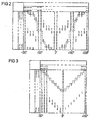
- FIGS. 2 and 3 illustrate the memory organization of the current shape memories SF2 (SF3) in the form of a matrix: an area address is assigned to each column of the matrix and a location address is assigned to each row. Each column contains a full period of the AC voltage as a sequence of 1 and 0. This sequence is read out periodically during the cyclical output of the location addresses, which creates a square-wave voltage, the 0-crossings of which are due to the position of the transitions from 1 to 0 and 0 to 1 in each column are determined. If the columns are now read out one after the other and the transitions 0/1 and 1/0 are located at different location addresses, this results in a square wave whose phase position changes. For example, if the one shown in FIG.
- phase position changes from -360 ° to + 360 ° according to an approximately sinusoidal function (see the dashed stair curve).
- a beat voltage then follows the same function, which results from the superimposition of the phase-modulated voltage thus obtained with an unmodulated AC voltage of the same center frequency - at output terminal A1.
- the latter AC voltage is tapped directly from the most significant digit of the r-digit address output of the location address transmitter PAG.
- phase modulation shown in FIG. 2 sometimes requires the same position of the 1/0 and 0/1 transitions in several columns.
- the same result can, however, be achieved by using a corresponding control of the area control part BST from the microcomputer with a smaller memory requirement by reading out the same column several times in succession before the area address counter BAZ advances to the next column.
- a halving of the beat frequency can also be achieved with the same read cycle.
- the beat frequency is doubled according to the same principle in that only half of the space addresses of one column and then the other half of space addresses are read from another column.
- the current shape memory SF2 (SF3) has a (eight) memory cells per memory location; accordingly, a columns form an area group with the same group address.
- the a columns (memory areas) with the same group address are read out in sequence using the SS2 (SS3) switch before switching to the next higher group address.
- the three least significant outputs of the area address counter BAZ2 (BAZ3) are connected to the respective position switch SS2 (SS3), which thereby controls each of the a outputs of the current form memory to the amplifier device V in sequence.
Landscapes
- Health & Medical Sciences (AREA)
- Animal Behavior & Ethology (AREA)
- Biomedical Technology (AREA)
- Nuclear Medicine, Radiotherapy & Molecular Imaging (AREA)
- Radiology & Medical Imaging (AREA)
- Life Sciences & Earth Sciences (AREA)
- Engineering & Computer Science (AREA)
- General Health & Medical Sciences (AREA)
- Public Health (AREA)
- Veterinary Medicine (AREA)
- Electrotherapy Devices (AREA)
- Ac-Ac Conversion (AREA)
- Surgical Instruments (AREA)
- Measurement And Recording Of Electrical Phenomena And Electrical Characteristics Of The Living Body (AREA)
Priority Applications (1)
| Application Number | Priority Date | Filing Date | Title |
|---|---|---|---|
| AT86111655T ATE57842T1 (de) | 1985-09-05 | 1986-08-22 | Reizstromgeraet zur erzeugung von mindestens zwei wechselspannungen. |
Applications Claiming Priority (2)
| Application Number | Priority Date | Filing Date | Title |
|---|---|---|---|
| DE3531739 | 1985-09-05 | ||
| DE3531739 | 1985-09-05 |
Publications (2)
| Publication Number | Publication Date |
|---|---|
| EP0214537A1 EP0214537A1 (de) | 1987-03-18 |
| EP0214537B1 true EP0214537B1 (de) | 1990-10-31 |
Family
ID=6280216
Family Applications (1)
| Application Number | Title | Priority Date | Filing Date |
|---|---|---|---|
| EP86111655A Expired - Lifetime EP0214537B1 (de) | 1985-09-05 | 1986-08-22 | Reizstromgerät zur Erzeugung von mindestens zwei Wechselspannungen |
Country Status (4)
| Country | Link |
|---|---|
| EP (1) | EP0214537B1 (da) |
| AT (1) | ATE57842T1 (da) |
| DE (1) | DE3675300D1 (da) |
| DK (1) | DK415286A (da) |
Family Cites Families (4)
| Publication number | Priority date | Publication date | Assignee | Title |
|---|---|---|---|---|
| DE2931638C2 (de) * | 1979-08-03 | 1982-12-16 | Siemens AG, 1000 Berlin und 8000 München | Interferenzstromtherapiegerät |
| DE2937984A1 (de) * | 1979-09-20 | 1981-04-02 | Robert Bosch Gmbh, 7000 Stuttgart | Schaltungsanordnung zum erzeugen zweier rechteckfoermiger wechselspannungen |
| DE3049530A1 (de) * | 1980-12-31 | 1982-07-29 | Deutsche Nemectron GmbH, 7500 Karlsruhe | Vorrichtung zur reizstromtherapie |
| DE3335849A1 (de) * | 1983-10-03 | 1985-04-18 | Siemens AG, 1000 Berlin und 8000 München | Interferenzstromtherapiegeraet |
-
1986
- 1986-08-22 AT AT86111655T patent/ATE57842T1/de not_active IP Right Cessation
- 1986-08-22 DE DE8686111655T patent/DE3675300D1/de not_active Expired - Lifetime
- 1986-08-22 EP EP86111655A patent/EP0214537B1/de not_active Expired - Lifetime
- 1986-09-01 DK DK415286A patent/DK415286A/da not_active Application Discontinuation
Also Published As
| Publication number | Publication date |
|---|---|
| EP0214537A1 (de) | 1987-03-18 |
| DE3675300D1 (de) | 1990-12-06 |
| DK415286A (da) | 1987-03-06 |
| ATE57842T1 (de) | 1990-11-15 |
| DK415286D0 (da) | 1986-09-01 |
Similar Documents
| Publication | Publication Date | Title |
|---|---|---|
| DE3003099C2 (de) | Digital-Analog-Wandler mit Kompensationsschaltung | |
| DE3329049A1 (de) | Datenuebertragungssystem | |
| DE2834387A1 (de) | Elektro-optische zeitanzeigeeinrichtung | |
| CH645473A5 (en) | Method for activating a liquid crystal display | |
| DE69213585T2 (de) | Signalpegel-Anzeigevorrichtung | |
| EP0214537B1 (de) | Reizstromgerät zur Erzeugung von mindestens zwei Wechselspannungen | |
| EP0029490B1 (de) | Verfahren zur Umwandlung von linear codierten digitalen Signalen in nicht linear codierte digitale Signale gemäss einer dem A-Gesetz oder dem My-Gesetz gehorchenden Mehrfachsegmentkennlinie | |
| DE68906959T2 (de) | Verfahren zur aus einer Steuereinheit quasiparallelen Steuerung einer Anzahl Peripherieeinheiten und System zum Durchführen dieses Verfahrens. | |
| EP0177803B1 (de) | Verfahren und Anordnung zum hochauflösenden Digitalisieren eines Signales | |
| DE2337132C3 (de) | Schaltungsanordnung zur Anzeige der Überschreitung wenigstens eines Grenzwertes durch ein digitales, binär codiertes Meßsignal | |
| EP0137936A1 (de) | Interferenzstromtherapiegerät | |
| CH669048A5 (de) | Verfahren zur messung des verhaeltnisses einer messgroessenabhaengigen kapazitaet zu einer referenzkapazitaet und einrichtung zur durchfuehrung des verfahrens. | |
| DE2343092A1 (de) | Programmierbarer funktionsgenerator | |
| DE2733875C2 (de) | Verfahren zur digitalen Informationsübertragung und Anordnung zur Durchführung des Verfahrens | |
| DE2424930C3 (de) | Anordnung zur Analog/Digitalumwandlung | |
| DE2804110C3 (de) | Elektronische Uhr | |
| DE2906471A1 (de) | Schaltungsanordnung zur sequentiellen erzeugung der funktionswerte mehrerer schwingungen, deren folgefrequenzen n-fache einer grundschwingung sind | |
| DE3142495C2 (de) | Digitaler Hörtongenerator | |
| DE3417816A1 (de) | Programmierbares schaltnetz | |
| CH620036A5 (en) | Liquid-crystal display device and use of the device as an oscillograph | |
| DE3019865A1 (de) | Elektronische uhr | |
| DE2319986C3 (de) | Digital-Analog-Umsetzer | |
| DE2825449C2 (de) | Statischer Rundsteuerempfänger | |
| DE3609430A1 (de) | Verfahren zur chronologisch richtigen registrierung von informationsinhalten einer vielzahl von informationsquellen | |
| DE2231216A1 (de) | Digital-Analog-Umsetzer |
Legal Events
| Date | Code | Title | Description |
|---|---|---|---|
| PUAI | Public reference made under article 153(3) epc to a published international application that has entered the european phase |
Free format text: ORIGINAL CODE: 0009012 |
|
| AK | Designated contracting states |
Kind code of ref document: A1 Designated state(s): AT CH DE GB LI NL |
|
| 17P | Request for examination filed |
Effective date: 19870407 |
|
| 17Q | First examination report despatched |
Effective date: 19900226 |
|
| GRAA | (expected) grant |
Free format text: ORIGINAL CODE: 0009210 |
|
| AK | Designated contracting states |
Kind code of ref document: B1 Designated state(s): AT CH DE GB LI NL |
|
| PG25 | Lapsed in a contracting state [announced via postgrant information from national office to epo] |
Ref country code: GB Effective date: 19901031 |
|
| REF | Corresponds to: |
Ref document number: 57842 Country of ref document: AT Date of ref document: 19901115 Kind code of ref document: T |
|
| REF | Corresponds to: |
Ref document number: 3675300 Country of ref document: DE Date of ref document: 19901206 |
|
| GBV | Gb: ep patent (uk) treated as always having been void in accordance with gb section 77(7)/1977 [no translation filed] | ||
| PG25 | Lapsed in a contracting state [announced via postgrant information from national office to epo] |
Ref country code: LI Effective date: 19910831 Ref country code: CH Effective date: 19910831 |
|
| PLBE | No opposition filed within time limit |
Free format text: ORIGINAL CODE: 0009261 |
|
| STAA | Information on the status of an ep patent application or granted ep patent |
Free format text: STATUS: NO OPPOSITION FILED WITHIN TIME LIMIT |
|
| 26N | No opposition filed | ||
| PG25 | Lapsed in a contracting state [announced via postgrant information from national office to epo] |
Ref country code: NL Effective date: 19920301 |
|
| NLV4 | Nl: lapsed or anulled due to non-payment of the annual fee | ||
| REG | Reference to a national code |
Ref country code: CH Ref legal event code: PL |
|
| PGFP | Annual fee paid to national office [announced via postgrant information from national office to epo] |
Ref country code: AT Payment date: 19940729 Year of fee payment: 9 |
|
| PG25 | Lapsed in a contracting state [announced via postgrant information from national office to epo] |
Ref country code: AT Effective date: 19950822 |
|
| PGFP | Annual fee paid to national office [announced via postgrant information from national office to epo] |
Ref country code: DE Payment date: 19970325 Year of fee payment: 11 |
|
| PG25 | Lapsed in a contracting state [announced via postgrant information from national office to epo] |
Ref country code: DE Free format text: LAPSE BECAUSE OF NON-PAYMENT OF DUE FEES Effective date: 19980501 |