EP0214476B1 - Verfahren und Schaltungsanordnung zum Übertragen von Datensignalen zwischen zwei zu einem Ringleitungssystem gehörenden Steuereinrichtungen - Google Patents
Verfahren und Schaltungsanordnung zum Übertragen von Datensignalen zwischen zwei zu einem Ringleitungssystem gehörenden Steuereinrichtungen Download PDFInfo
- Publication number
- EP0214476B1 EP0214476B1 EP86110945A EP86110945A EP0214476B1 EP 0214476 B1 EP0214476 B1 EP 0214476B1 EP 86110945 A EP86110945 A EP 86110945A EP 86110945 A EP86110945 A EP 86110945A EP 0214476 B1 EP0214476 B1 EP 0214476B1
- Authority
- EP
- European Patent Office
- Prior art keywords
- signal
- block
- control device
- address
- arrangement
- Prior art date
- Legal status (The legal status is an assumption and is not a legal conclusion. Google has not performed a legal analysis and makes no representation as to the accuracy of the status listed.)
- Expired - Lifetime
Links
- 238000000034 method Methods 0.000 title claims abstract description 20
- 230000005540 biological transmission Effects 0.000 title claims abstract description 16
- 238000012545 processing Methods 0.000 claims abstract description 4
- 238000011156 evaluation Methods 0.000 claims abstract description 3
- 101100301524 Drosophila melanogaster Reg-5 gene Proteins 0.000 claims description 10
- 101100412401 Rattus norvegicus Reg3a gene Proteins 0.000 claims description 8
- 238000012546 transfer Methods 0.000 claims description 7
- 102100031438 E3 ubiquitin-protein ligase RING1 Human genes 0.000 claims description 3
- 101000707962 Homo sapiens E3 ubiquitin-protein ligase RING1 Proteins 0.000 claims description 3
- 208000035217 Ring chromosome 1 syndrome Diseases 0.000 claims description 3
- 230000008859 change Effects 0.000 claims description 3
- 238000012217 deletion Methods 0.000 claims description 2
- 230000037430 deletion Effects 0.000 claims description 2
- 230000000694 effects Effects 0.000 claims description 2
- 210000000352 storage cell Anatomy 0.000 claims 6
- 230000003213 activating effect Effects 0.000 claims 1
- 230000004044 response Effects 0.000 abstract description 3
- 230000008569 process Effects 0.000 description 8
- 101100120298 Rattus norvegicus Flot1 gene Proteins 0.000 description 5
- 101100412403 Rattus norvegicus Reg3b gene Proteins 0.000 description 5
- 238000013475 authorization Methods 0.000 description 5
- 102100023882 Endoribonuclease ZC3H12A Human genes 0.000 description 3
- 101710112715 Endoribonuclease ZC3H12A Proteins 0.000 description 3
- 230000008054 signal transmission Effects 0.000 description 3
- 101150103187 Reg4 gene Proteins 0.000 description 2
- 230000008901 benefit Effects 0.000 description 2
- 230000000903 blocking effect Effects 0.000 description 2
- 238000010586 diagram Methods 0.000 description 2
- 101100102598 Mus musculus Vgll2 gene Proteins 0.000 description 1
- 102100023477 Transcription cofactor vestigial-like protein 2 Human genes 0.000 description 1
- 238000004891 communication Methods 0.000 description 1
- 230000001419 dependent effect Effects 0.000 description 1
- 238000001514 detection method Methods 0.000 description 1
- 230000006870 function Effects 0.000 description 1
- 230000003993 interaction Effects 0.000 description 1
- 230000007246 mechanism Effects 0.000 description 1
- 239000013307 optical fiber Substances 0.000 description 1
- 230000000717 retained effect Effects 0.000 description 1
- 230000011664 signaling Effects 0.000 description 1
Images


Classifications
-
- H—ELECTRICITY
- H04—ELECTRIC COMMUNICATION TECHNIQUE
- H04L—TRANSMISSION OF DIGITAL INFORMATION, e.g. TELEGRAPHIC COMMUNICATION
- H04L12/00—Data switching networks
- H04L12/28—Data switching networks characterised by path configuration, e.g. LAN [Local Area Networks] or WAN [Wide Area Networks]
- H04L12/42—Loop networks
- H04L12/427—Loop networks with decentralised control
- H04L12/433—Loop networks with decentralised control with asynchronous transmission, e.g. token ring, register insertion
-
- H—ELECTRICITY
- H04—ELECTRIC COMMUNICATION TECHNIQUE
- H04L—TRANSMISSION OF DIGITAL INFORMATION, e.g. TELEGRAPHIC COMMUNICATION
- H04L1/00—Arrangements for detecting or preventing errors in the information received
- H04L1/12—Arrangements for detecting or preventing errors in the information received by using return channel
- H04L1/16—Arrangements for detecting or preventing errors in the information received by using return channel in which the return channel carries supervisory signals, e.g. repetition request signals
- H04L1/1607—Details of the supervisory signal
- H04L1/1671—Details of the supervisory signal the supervisory signal being transmitted together with control information
-
- H—ELECTRICITY
- H04—ELECTRIC COMMUNICATION TECHNIQUE
- H04L—TRANSMISSION OF DIGITAL INFORMATION, e.g. TELEGRAPHIC COMMUNICATION
- H04L1/00—Arrangements for detecting or preventing errors in the information received
- H04L2001/0092—Error control systems characterised by the topology of the transmission link
- H04L2001/0095—Ring
Definitions
- the invention relates to a method and a circuit arrangement for transmitting data signals between control devices connected to one another via a clock-controlled, directionally dependent ring line system, according to the preamble of claim 1 and claim 2.
- the method according to claim 1 has the advantage that the received signal block is used directly for the generation of an acknowledgment signal intended for the transmitter of a signal block just received, by deleting the block start identifier belonging to the signal block only to the transmitter address identified by the block end identifier an acknowledgment signal relating to the reception of the signal block is added.
- the forwarded signal block is no longer identified as such by the deletion of the block start identifier.
- the sender address transmitted in connection with the block end identifier can also be seen, to which an acknowledgment signal relating to the reception of the signal block is appended by the control device selected as the receiver. In the control device from which the signal block was previously delivered, it is therefore only necessary to monitor the occurrence of the sender address in connection with the end of block identification in order to take over the acknowledgment signal intended for it.
- the circuit arrangement according to claim 2 has a reception control and a receiver arrangement consisting of a reception memory for the reception of signal blocks and an acknowledgment receiver.
- Claims 7 and 8 relate to advantageous refinements of the reception control and the receipt receiver.
- the reception control and the receipt receiver are characterized both by a low outlay in terms of circuitry and by a low outlay on control.
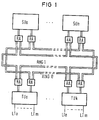
- FIG. 1 shows a data switching system with a plurality of switching units SUO to SUn. These switching units perform the switching functions required for the transmission of data signals based on the load sharing principle.
- the switching units are jointly connected to a ring line system.
- a ring line system can consist of a single closed ring line arrangement.
- Such a ring line system can, however, as shown in FIG. 1, for example, be made up of two parallel, independent ring line arrangements RING0 and RING1.
- Such redundancy makes it possible, for example, if one of the ring line arrangements fails, to carry out the transmission of signal blocks and acknowledgment signals on the other ring line arrangement.
- connection of the mentioned switching units SU0 to SUn The two ring line arrangements are each carried out via an interface circuit RA which is separate for each of the ring line arrangements and which will be discussed in more detail below.
- a plurality of line connection units TU0 to TUk are in each case connected to the ring line arrangements RING0 and RING1 again via an interface circuit RA separate for each of the ring line arrangements.
- These line connection units together with the associated interface circuits, serve for the data signal transmission between the aforementioned switching units and transmission lines connected to subscriber devices, which are connected to the line connection units TU0 to TUk.
- Each of the line connection units has a plurality of line connections LT0 to Ltm for such a connection of transmission lines.
- the circuit units formed from the aforementioned switching units or the line connection units and the associated interface circuits are also referred to below as control devices.
- control devices In the event that the ring line system consists of only one ring line arrangement, only one interface circuit belongs to a control device.
- data signals are transmitted in the form of signal blocks, each of which as data signals in the course of establishing a connection, signaling information and, in the case of an established connection, that between the subscriber devices in question have transmitting message signals.
- Each signal block to be transmitted contains in addition to the actual data signals, each consisting of a plurality of bits, e.g. B. 8 bits, are formed, at least one of the control devices as a receiver address, a start identifier denoting the start of a signal block, an end identifier denoting the end of a signal block, a sender address denoting the control unit emitting the signal block and at least one acknowledgment signal or an empty receipt.
- a signal block constructed in this way can only be delivered to one of the ring line arrangements if the control device in question has previously received a transmission authorization signal transmitted from control device to control device and controlling it in a transmission authorization state.
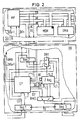
- FIG. 2 shows the structure of a control device in greater detail.
- a control device consists either of a switching unit or of a line connection unit, indicated in FIG. 2 by the designation SU / TU, and a number of interface circuits RA corresponding to the number of ring line arrangements. Only one of these interface circuits is shown in FIG. 2, since all of the interface circuits connected to the switching units or line connection units have the same internal structure.
- the unit shown in FIG. 2 with SU / TU and shown in sections has a microprocessor arrangement which controls both transmission and reception processes.
- Microprocessor MP a read-only memory (program memory) and read / write memory comprising memory arrangement MEM and a device for direct memory access DMA.
- the memory arrangement and the latter device are connected to the microprocessor MP via a bus line system.
- the bus line system consists of a data bus DB, an address bus AB and a control bus SB.
- the interface circuit RA is also connected to the microprocessor MP via the data bus and the lines of the control bus labeled RD and BC.
- INTn-1 and INTn lead to interrupt inputs IN-Tn-1 and INTn of the microprocessor MP.
- the interface circuit RA is connected to the device for direct memory access DMA via a further line labeled DMA.
- An interface circuit RA has both devices for the treatment of received signal blocks and acknowledgment signals and devices for the transmission of signal blocks available in the associated control device. In FIG. 2, of these devices, only the devices relating to the treatment of received signal blocks and acknowledgment signals relating to the present invention are shown.
- the interface circuit RA shown in FIG. 2 has a receive register Reg1 at the interface to the associated ring line arrangement, which may be the ring line arrangement RING0, for example, which receives signals transmitted in parallel via the ring line arrangement.
- This register is controlled by a clock generator, which Feeds clock signals corresponding to the transmission speed of the ring line arrangement to a clock input of the input register Reg1 via a line T.
- This input register is connected on the output side via a line arrangement ED on the one hand to a receive buffer arrangement EP and on the other hand to first inputs of a data switch DW1.
- the receive buffer arrangement serves, as will be explained in the following, for receiving signal blocks and acknowledgment signals and for forwarding them to the control device downstream in the ring line system.
- the receive buffer arrangement EP is connected to the unit SU / TU via the data bus DB, the lines RD and BC of the control bus SB already mentioned and via the lines DMA and INTn-1.
- the receive buffer arrangement receives clock signals via the already mentioned line T and itself outputs control signals via lines QE, QD, QK and F to a status register ZReg and via a line TL to a clock input of a register Reg2 serving as an acknowledgment receiver.
- the receive buffer arrangement is connected via a line arrangement ED 'to first inputs of a further data switch DW2.
- Second inputs of the data switch DW2 and data switch DW1 just mentioned are connected to outputs of the status register ZReg. Both data switches are controlled by the status register via lines SL1 and SL2.
- the data switch DW1 is connected to signal inputs of the already mentioned register Reg2, which is connected with its signal outputs to the data bus DB.
- the data switch DW2, on the other hand, is connected on the output side to signal inputs of an output register Reg3.
- This register receives Via the line T clock signals are supplied and at its signal outputs from the data switch DW2 signals supplied to the ring line arrangement connected to the interface circuit RA.
- the signal inputs of the output register are, moreover, also connected to devices for sending signal blocks available in the associated control device. However, as already mentioned, the structure of these facilities is not discussed in detail.
- data signals can optionally be transmitted to a single control device selected as a receiver or to a group of control devices. It is initially assumed that data signals from a control device of the ring line system are only to be transmitted to a single control device. For this transmission, the control device, from which the data signals are to be delivered, assembles the data signals in the associated unit SU / TU into a signal block. Such a signal block is shown schematically in FIG. 5a. It is initiated by a recipient address EADR which designates the control device selected as the recipient. The data signals DS1 to DSn to be transmitted follow this receiver address. Attached to these data signals is a transmitter address SADR that designates the control unit sending this signal block as a transmitter.
- SADR transmitter address
- a first identification bit designated A in FIG. 5, serves to identify the start of a signal block.
- the identification bit labeled E serves to identify the end of a signal block.
- the start and end of a signal block may be indicated, for example, by the logic state "1" of the respective identification bit.
- the logical state "1" of the identification bit A is referred to below as the block start identifier and the logical state "1" of the identification bit E as the block end identifier.
- the block start identifier is transmitted together with the recipient address and the block end identifier together with the sender address.
- a signal block compiled in the manner just described is then output upon arrival of a transmission authorization signal transmitted from the control device to the control device and controlling it in a transmission authorization state from the unit SU / TU (FIG. 2) via the output register Reg3 to the ring line arrangement connected to the interface circuit RA .
- Each of the interface circuits connected to the ring line arrangement receives the signals belonging to the transmitted signal block via the input register Reg1.
- a comparison is made of the receiver address transmitted in the signal block together with the block start identifier with the address assigned to the respective control device within the ring line system.
- the respective receive buffer arrangement EP continues to receive the received signal block unchanged via the line arrangement ED 'to the data switch DW2.
- the signal block then arrives at the ring line arrangement again via this and the output register Reg3.
- the signal block just received is copied in the receive buffer arrangement EP.
- the signal block itself is forwarded to the control device following in the ring line system by deleting the block start identifier (A) via the line arrangement ED '.
- the status register ZReg adds an acknowledgment signal (EADR, QS) to the transmitter address (SADR), so that the empty acknowledgment (LQ) originally contained in the signal block is overwritten.
- the status register ZReg receives a control signal from the receive buffer arrangement EP, which monitors the occurrence of the end-of-block identifier (E) and the sender address (SADR), via the line QE.
- the transmitted signal block is shown in FIG 5b.
- the reception buffer arrangement EP After the copying of a signal block mentioned, the reception buffer arrangement EP outputs a control signal indicating the availability of a received signal block via the line DMA to the device for direct memory access DMA. This device then causes the relevant signal block to be transferred to the SU / TU unit. The end of the signal block is indicated to the microprocessor MP by an interrupt signal at its interrupt input INTn-1 from the receive buffer arrangement EP.
- the block start identifier (A) originally transmitted in the signal block is deleted when it is forwarded, the signal block is no longer recognized as such, so that it cannot be picked up by subsequent control devices. Only the sender address (SADR) transmitted together with the block end identifier (E) can still be recognized as such.
- SADR sender address
- the occurrence of the end-of-block identifier and the sender address is monitored in the control device from which the signal block just acknowledged was previously delivered, specifically in the associated receive buffer arrangement EP. If the occurrence of end-of-block identification and sender address is recognized by the latter, it outputs a control signal via line TL to the associated acknowledgment register Reg2, which then receives the acknowledgment signal QS transmitted after the sender address from line arrangement ED via data switch DW1. Upon receipt of such an acknowledgment signal, the acknowledgment register issues an interrupt signal to the microprocessor MP via the line INTn. On the basis of this signal, the latter then accepts the acknowledgment signal available in the acknowledgment register for evaluation. A send process is now
- a signal block is to be transmitted to a group of control devices.
- a signal block is first compiled in the control device emitting the signal block in the manner shown in FIG. 5a and delivered to the ring line arrangement.
- the recipient address now designates a group of control devices.
- a group can optionally include all of the control devices belonging to the ring line arrangement or only a part of these control devices.
- the microprocessor MP of the control device in question also sends a broadcast signal BC to the receive buffer arrangement EP via the line of the same name.
- This broadcast signal indicates that a signal block has been delivered to a group of control devices.
- the signal block is again transmitted in the manner shown from control device to control device.
- Control devices that are not designated by the recipient address pass on the received signal block unchanged.
- the first control device belonging to the group designated by the recipient address copies the received signal block in the associated receive buffer arrangement EP.
- the signal block itself is passed on to the control device following in the ring line arrangement, omitting the previous block end identifier (E).
- the status register ZReg adds an acknowledgment information together with a block end identifier to the transmitter address (SADR) in response to a control signal emitted by the receive buffer arrangement, which is transmitted via the line QK.
- SADR transmitter address
- the acknowledgment information consists of the address (EADR1) assigned to the relevant control device within the ring line arrangement and the actual acknowledgment signal (QS1) relating to the reception of the signal block.
- the signal block emitted by the first control device belonging to the group is shown in FIG. 5c.
- the data switch DW2 shown in FIG. 2 is controlled accordingly via the line SL1 from the status register ZReg.
- the received signal block is copied to control devices and passed on to the control device following in the loop system, omitting the previous block end identifier. Acknowledgment information and a block end identifier are added to the last acknowledgment information transmitted in the signal block.
- the signal block emitted by the m-th control unit belonging to the group is shown in FIG. 5d. It follows from this that the signal block which the last control device belonging to the group emits has acknowledgment information for all control devices belonging to the group.
- the signal block containing the acknowledgment signals of all control devices belonging to the group is adopted in the control device from which the original signal block was emitted.
- This transfer can in turn take place in the form of a copying process in the associated receive buffer arrangement EP, to which a broadcast signal BC was supplied when the signal block was originally delivered.
- the copying process is initiated upon the occurrence of the block start identifier together with the broadcast signal.
- the signal block itself is returned to the associated ring line arrangement by deleting both the block start identifier and the block end identifier via the output register Reg3. Since both identifiers have now been deleted, the transmitted signal block can no longer be recognized by the control devices following in the ring line arrangement.
- the Receive buffer arrangement EP After copying the signal block including the acknowledgment information, ie when the end of block identification associated with this signal block occurs, the Receive buffer arrangement EP via the line QD from a control signal to the associated status register ZReg.
- This status register then provides an acknowledgment signal relating to the reception of this signal block, which is transferred to the acknowledgment register Reg2 via the data switch DW1.
- the acknowledgment register receives a corresponding control signal from the receive buffer arrangement via line TL.
- the data switch DW1 is controlled accordingly for this transfer from the status register ZReg via the line SL2.
- the receive buffer arrangement contains a read / write memory RAM with a plurality of memory cells for receiving signal blocks, including the associated block end identifiers.
- This memory is connected with its data signal inputs / outputs on the one hand for the reception of signal blocks with the line arrangement ED already shown in FIG. 2 and on the other hand for the delivery of signal blocks via a register Reg4 to the data bus DB also provided in FIG. He receives for the delivery of a signal block Reading clocks supplied via the line RD belonging to the control bus SB. These reading cycles correspond to the working speed of the respective control device.
- the read / write memory RAM is supplied with write clocks at an input WR. These write clocks occur on line T and are output via an AND gate G1 to the aforementioned input of the memory.
- This AND gate is controlled into the transferable state by a control signal appearing on a line ANF. This control signal is emitted by a receiving control EPS.
- the read / write memory is connected with its address inputs via a data switch DW3 on the one hand to a counter LZ and on the other hand to a counter SZ.
- the counter SZ serving as a write counter is connected with its clock input to the output of the previously mentioned AND gate G1, ie it receives the write clocks simultaneously with the read / write memory RAM.
- the counter SZ outputs its counter readings, which change in accordance with these write cycles, as address signals for the read / write memory.
- These counter outputs are also connected to a register Reg5, which receives a takeover clock via an AND gate G2.
- This AND gate is connected on the input side to line T and a line AK connected to the reception controller EPS.
- register Reg5 is connected to set inputs of counter SZ. These set inputs are released by a set signal appearing on a line F and output by the reception controller EPS.
- the counter LZ serves as a read counter. It receives the reading cycles occurring on line RD at its clock input and outputs its counter readings, which change according to these reading cycles, as address signals when reading a signal block to the read / write memory RAM.
- the data switch DW3 connected to the two counters mentioned is also connected to the line ANF with its control input.
- the receive buffer arrangement EP has a further counter IZ.
- This counter is an up / down counter which receives write clocks for counting in the one direction from the output of the AND gate G1 and for reading in the other direction the read clocks occurring on line RD.
- the counter IZ is connected to inputs of a decoder DEC, which at a specific counter reading of the counter IZ emits a message signal to the reception controller EPS via a line SUE.
- the counter IZ is also connected to a register Reg6 and to an OR gate G3.
- the register Reg6 receives a takeover clock at a clock input from the AND gate G2.
- this register is connected to set inputs of the counter IZ, which are released again by a set signal occurring on line F.
- OR gate G3 The output of the aforementioned OR gate G3 is connected to first inputs of an OR gate G4.
- This OR gate is connected to the negating output of a flip-flop FF with a further input.
- the output of the OR gate G4 is on line DMA connected.
- the non-negating output of flip-flop FF on the other hand, is connected to line INTn-1.
- the clock input of this flip-flop receives the reading clocks occurring on line RD.
- the data input of the flip-flop is connected to the line EK of the data bus DB which carries the block end identifier.
- the already mentioned receive control EPS is connected to a plurality of the lines shown in FIG. 2.
- these are the line arrangement ED and the lines BC and T.
- On the output side there is a connection on the one hand to the line arrangement ED 'and on the other hand to the lines TL, QE, QD, QK and F.
- the reception controller EPS emits a control signal via the line ANF.
- write / read memory RAM and the two counters SZ and IZ are supplied with write pulses for the reception of a received signal block via AND gate G1.
- Both counters may initially be in a basic counter reading, which may be counter reading "0", for example.
- the counter status is then changed with each write cycle, the memory cells of the read / write memory RAM being continuously addressed with the changing current counter status of the counter SZ, while the current counter status of the counter IZ corresponds to the current fill level of the read / write memory corresponds.
- the presence of a received signal block from the unit SU / TU is indicated by a control signal transmitted via the line DMA.
- the signal block located in the read / write memory is then converted into the unit by supplying read clocks via the line RD and continuously addressing the memory cells of the read / write memory from the counter LZ by means of direct memory access via the register Reg4 SU / TU taken over until the block end identifier contained in the signal block just read occurs.
- This end of block identifier occurs on line EK1 of data bus DB.
- This occurrence brings the flip-flop FF into its active state, in which it signals the microprocessor the end of a signal block via the line INTn-1.
- the microprocessor then interrupts the supply of further reading cycles.
- the flip-flop FF interrupts the control signal transmitted via line DMA for direct memory access.
- the counter LZ may also begin to count from a predetermined basic counter reading, which may also be the counter reading "0". The instantaneous counter reading which is then given by the counter LZ when the end of the block occurs occurs until a further reading process is initiated.
- the read clocks are also fed to the counter IZ. These reading cycles cause counting in the reverse direction, so that the current counter reading of this counter is reduced with each reading cycle.
- the current counter reading thus corresponds to the number of signals in the signal block which have not yet been read from the read / write memory.
- the OR gate G4 is blocked so that the supply of the control signal transmitted via the line DMA is interrupted.
- the control processes already explained also run again.
- the counters SZ, LZ and IZ continue to count from their pending counter readings.
- the initial counter readings of these counters now correspond to the counter readings last reached when transferring or reading out signal blocks.
- the rewriting of signal blocks in the read / write memory can also take place at a point in time at which previously received signal blocks have not yet or not yet been completely adopted into the unit SU / TU. In this case, the recording of a signal block just received has priority over the reading of previously received signal blocks.
- the counter IZ changes its counter reading in accordance with the number of memory cells in the read / write memory RAM which are occupied by signals from the signal blocks and have not yet been read out.
- a signal transmitted via line AK is used to indicate the occurrence of the block start identifier transmitted with it issued a takeover clock via the AND gate G2 to the two registers REG5 and Reg6. Each of these then takes over the current counter reading given by its associated counter as the initial counter reading for a further recording of signal blocks.
- the decoder does so DEC forth a message signal to the receiving controller EPS, which then transmits via the line F a set signal for the release of the set inputs of the counters SZ and IZ.
- the initial counter readings transferred to registers Reg5 and Reg6 at the beginning of the signal block just received are thus transferred to counters SZ and IZ, i.e. the memory cells of the write / store RAM, which have already been occupied by signals from the signal block which cannot be completely recorded, are released again.
- the recording of the signal block just received in the read / write memory is ended. This is done by blocking the AND gate G1 on the basis of a control signal transmitted via the line ANF.
- the incomplete recording of a signal block is also signaled via line F to the status register ZReg shown in FIG. 2, which then appends a corresponding acknowledgment signal to the transmitter address transmitted with the signal block just received.
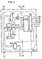
- FIG. 4 shows the structure of the reception control EPS.
- This contains two comparator arrangements Vg11 and Vg12 for comparing the receiver address transmitted in a signal block together with the block start identifier or that together with an acknowledgment signal Transmitted sender address with an address assigned to the associated control device within the ring line arrangement.
- the comparator arrangement Vg11 is used for an address comparison when a signal block intended only for one of the control devices is received and when an acknowledgment signal is received.
- the comparator arrangement VGL2, on the other hand is used for address comparison when a signal block intended for a group of control devices is received.
- the comparison address to be used for the respective comparison is provided by an arrangement S1 or S2, which is connected to the comparator arrangement Vg11 or Vg12 and is represented as a switch arrangement. These arrangements can be any storage devices.
- the comparator arrangement to be used for an address comparison is controlled by a signal on line GA. This signal is part of the receiver address that designates a group of control devices and designates it as such.
- the outputs of the two comparator arrangements are connected via an OR gate G5 to one of the address inputs of a read-only memory PROM. Further address inputs of this memory are connected to a line AK carrying the block start identifier, a line EK2 carrying the block end identifier, the lines SUE, BC and to the output of the comparator arrangement Vg12.
- the two lines AK and EK2 are associated with the line arrangement ED.
- the read-only memory PROM has a plurality of memory locations in which all control signals for the treatment of received signal blocks and acknowledgment signals are stored.
- This read-only memory is connected to a register Reg7 with its data outputs.
- This register is connected via data outputs to the lines ANF, QE, QD, QK, TL and F already shown in FIG.
- a data output is also connected to a first control input of a Reg8 register.
- the register is Reg7 with a clock input finally connected to line T.
- a second control input of the register Reg8 is connected to the line BC already shown in FIG. This register is connected on the input side to the line arrangement ED and on the output side to the line arrangement ED '.
- the read-only memory PROM Depending on the signals that the read-only memory PROM is currently receiving at its address inputs, it emits a control signal corresponding to these signals, which is accepted by the register Reg7 and sent to the line in question.
- the effect of the control signals occurring on the lines ANF, QE, QD, QK, TL and F has already been explained with reference to FIG. 2.
- Each of the signal blocks received by the associated control device is forwarded via register Reg8 to the control device downstream in the ring line arrangement.
- the signal block in question is possibly treated with regard to the block start identifier and block end identifier contained in it.
- the treatment consists, as already mentioned above, in that, depending on the type of signal block to be forwarded, the block start identifier, the block end identifier or both identifiers are deleted.
Landscapes
- Engineering & Computer Science (AREA)
- Computer Networks & Wireless Communication (AREA)
- Signal Processing (AREA)
- Small-Scale Networks (AREA)
- Communication Control (AREA)
- Selective Calling Equipment (AREA)
- Exchange Systems With Centralized Control (AREA)
- Use Of Switch Circuits For Exchanges And Methods Of Control Of Multiplex Exchanges (AREA)
- Arrangements For Transmission Of Measured Signals (AREA)
- Apparatus For Radiation Diagnosis (AREA)
Priority Applications (1)
| Application Number | Priority Date | Filing Date | Title |
|---|---|---|---|
| AT86110945T ATE64804T1 (de) | 1985-09-11 | 1986-08-07 | Verfahren und schaltungsanordnung zum uebertragen von datensignalen zwischen zwei zu einem ringleitungssystem gehoerenden steuereinrichtungen. |
Applications Claiming Priority (2)
| Application Number | Priority Date | Filing Date | Title |
|---|---|---|---|
| DE3532460 | 1985-09-11 | ||
| DE3532460 | 1985-09-11 |
Publications (2)
| Publication Number | Publication Date |
|---|---|
| EP0214476A1 EP0214476A1 (de) | 1987-03-18 |
| EP0214476B1 true EP0214476B1 (de) | 1991-06-26 |
Family
ID=6280708
Family Applications (1)
| Application Number | Title | Priority Date | Filing Date |
|---|---|---|---|
| EP86110945A Expired - Lifetime EP0214476B1 (de) | 1985-09-11 | 1986-08-07 | Verfahren und Schaltungsanordnung zum Übertragen von Datensignalen zwischen zwei zu einem Ringleitungssystem gehörenden Steuereinrichtungen |
Country Status (14)
| Country | Link |
|---|---|
| US (1) | US4700018A (enExample) |
| EP (1) | EP0214476B1 (enExample) |
| JP (1) | JP2818163B2 (enExample) |
| AT (1) | ATE64804T1 (enExample) |
| AU (1) | AU588364B2 (enExample) |
| BR (1) | BR8604336A (enExample) |
| CA (1) | CA1266920A (enExample) |
| DE (1) | DE3679949D1 (enExample) |
| ES (1) | ES2002316A6 (enExample) |
| GR (1) | GR862300B (enExample) |
| IN (1) | IN166388B (enExample) |
| PT (1) | PT83341B (enExample) |
| YU (1) | YU158186A (enExample) |
| ZA (1) | ZA866882B (enExample) |
Families Citing this family (3)
| Publication number | Priority date | Publication date | Assignee | Title |
|---|---|---|---|---|
| EP0215276B1 (de) * | 1985-09-11 | 1991-06-26 | Siemens Aktiengesellschaft | Verfahren und Schaltungsanordnung zum Übertragen von Datensignalen an eine Gruppe von zu einem Ringleitungssystem gehörenden Steuereinrichtungen |
| ATE225585T1 (de) * | 1994-05-09 | 2002-10-15 | Europlex Res Ltd | Ringnetzsystem |
| GB2289394B (en) * | 1994-05-09 | 1998-06-10 | Europlex Res Ltd | A ring network system |
Family Cites Families (7)
| Publication number | Priority date | Publication date | Assignee | Title |
|---|---|---|---|---|
| CH591190A5 (enExample) * | 1975-04-25 | 1977-09-15 | Hasler Ag | |
| JPS607812B2 (ja) * | 1977-07-11 | 1985-02-27 | 富士電機株式会社 | デ−タバツフアリング装置 |
| DE3136495A1 (de) * | 1981-09-15 | 1983-03-24 | Siemens AG, 1000 Berlin und 8000 München | Verfahren und schaltungsanordnung zum uebertragen voninformationssignalen zwischen ueber ein richtungsabhaengig betriebenes ringleitungssystem miteinander verbundenen steuereinrichtungen |
| DE3136586A1 (de) * | 1981-09-15 | 1983-03-31 | Siemens AG, 1000 Berlin und 8000 München | Verfahren und schaltungsanordnung zum uebertragen von signalen zwischen beliebigen steuereinrichtungen eines taktgesteuerten, richtungsabhaengig betriebenen ringleitungssystems |
| JPS60132441A (ja) * | 1983-12-21 | 1985-07-15 | Hitachi Ltd | デ−タ伝送方法 |
| DE3679948D1 (de) * | 1985-09-11 | 1991-08-01 | Siemens Ag | Schaltungsanordnung zum uebertragen von datensignalen zwischen ueber ein ringleitungssystem miteinander verbundenen steuereinrichtungen. |
| EP0215276B1 (de) * | 1985-09-11 | 1991-06-26 | Siemens Aktiengesellschaft | Verfahren und Schaltungsanordnung zum Übertragen von Datensignalen an eine Gruppe von zu einem Ringleitungssystem gehörenden Steuereinrichtungen |
-
1986
- 1986-08-07 DE DE8686110945T patent/DE3679949D1/de not_active Expired - Lifetime
- 1986-08-07 AT AT86110945T patent/ATE64804T1/de not_active IP Right Cessation
- 1986-08-07 EP EP86110945A patent/EP0214476B1/de not_active Expired - Lifetime
- 1986-08-26 IN IN649/CAL/86A patent/IN166388B/en unknown
- 1986-08-27 US US06/900,900 patent/US4700018A/en not_active Expired - Lifetime
- 1986-09-09 GR GR862300A patent/GR862300B/el unknown
- 1986-09-09 CA CA000517748A patent/CA1266920A/en not_active Expired - Lifetime
- 1986-09-10 ZA ZA866882A patent/ZA866882B/xx unknown
- 1986-09-10 BR BR8604336A patent/BR8604336A/pt not_active IP Right Cessation
- 1986-09-10 JP JP61211826A patent/JP2818163B2/ja not_active Expired - Lifetime
- 1986-09-10 PT PT83341A patent/PT83341B/pt not_active IP Right Cessation
- 1986-09-10 YU YU01581/86A patent/YU158186A/xx unknown
- 1986-09-10 AU AU62535/86A patent/AU588364B2/en not_active Ceased
- 1986-09-11 ES ES8601820A patent/ES2002316A6/es not_active Expired
Also Published As
| Publication number | Publication date |
|---|---|
| DE3679949D1 (de) | 1991-08-01 |
| JP2818163B2 (ja) | 1998-10-30 |
| PT83341A (pt) | 1986-10-01 |
| ZA866882B (en) | 1987-04-29 |
| AU588364B2 (en) | 1989-09-14 |
| BR8604336A (pt) | 1987-05-12 |
| CA1266920A (en) | 1990-03-20 |
| GR862300B (en) | 1987-01-12 |
| PT83341B (pt) | 1992-10-30 |
| YU158186A (en) | 1989-02-28 |
| US4700018A (en) | 1987-10-13 |
| JPS6262694A (ja) | 1987-03-19 |
| ATE64804T1 (de) | 1991-07-15 |
| AU6253586A (en) | 1987-03-12 |
| ES2002316A6 (es) | 1988-08-01 |
| EP0214476A1 (de) | 1987-03-18 |
| IN166388B (enExample) | 1990-04-28 |
Similar Documents
| Publication | Publication Date | Title |
|---|---|---|
| DE3043894C2 (enExample) | ||
| DE69916937T2 (de) | Eingang-ausgangsuntersystem eines steuersystems | |
| DE3127321C2 (enExample) | ||
| DE69031266T2 (de) | Übertragungsarchitektur für Hochgeschwindigkeitsnetzwerk | |
| DE4104601C2 (de) | Empfangsdatenverarbeitungsanlage | |
| DE3642324C2 (de) | Multiprozessoranlage mit Prozessor-Zugriffssteuerung | |
| EP0329005B1 (de) | Verfahren zum Einrichten von über Koppelvielfache einer mehrstufigen Koppelanordnung verlaufenden virtuellen Verbindungen | |
| DE2943149C2 (de) | Ringnetzwerk mit mehreren an eine Daten-Ringleitung angeschlossenen Prozessoren | |
| DE3301628A1 (de) | Schaltungsanordnung fuer den datenaustausch zwischen zwei rechnern | |
| EP0453607A1 (de) | Verfahren und Schaltungsanordnung zur Reduzierung des Verlustes von Nachrichtenpaketen, die über eine Paketvermittlungseinrichtung übertragen werden | |
| DE69032723T2 (de) | FIFO mit variablem Zuweisungszeiger | |
| EP0214474B1 (de) | Verfahren und Schaltungsanordnung zum Ubertragen von Datensignalen zwischen über ein Ringleitungssystem miteinander verbundenen Steuereinrichtungen | |
| EP0453606B1 (de) | Verfahren und Schaltungsanordnung zur Reduzierung des Verlustes von Nachrichtenpaketen, die über eine Paketvermittlungseinrichtung übertragen werden | |
| DE3400464A1 (de) | Datenuebertragungssystem | |
| DE2027159B2 (de) | Datenverarbeitungsanlage | |
| EP0215276B1 (de) | Verfahren und Schaltungsanordnung zum Übertragen von Datensignalen an eine Gruppe von zu einem Ringleitungssystem gehörenden Steuereinrichtungen | |
| EP0214476B1 (de) | Verfahren und Schaltungsanordnung zum Übertragen von Datensignalen zwischen zwei zu einem Ringleitungssystem gehörenden Steuereinrichtungen | |
| EP0009600B1 (de) | Verfahren und Schnittstellenadapter zum Durchführen von Wartungsoperationen über eine Schnittstelle zwischen einem Wartungsprozessor und einer Mehrzahl einzeln zu prüfender Funktionseinheiten eines datenverarbeitenden Systems | |
| DE3788417T2 (de) | Verfahren zur Datenübertragungssteuerung. | |
| DE68925524T2 (de) | System zum Detektieren, dass Daten in einem Pufferspeicher gelöscht worden sind, insbesondere für einen Datenschalter | |
| EP0214475B1 (de) | Schaltungsanordnung zum Übertragen von Datensignalen zwischen über ein Ringleitungssystem miteinander verbundenen Steuereinrichtungen | |
| DE3136586C2 (enExample) | ||
| DE3329228A1 (de) | Datenuebertragungsverfahren in einem digitalen uebertragungsnetzwerk und vorrichtung zur durchfuehrung des verfahrens | |
| EP0214473B1 (de) | Schaltungsanordnung zum Übertragen von Datensignalen zwischen, über ein Ringleitungssystem miteinander verbundenen Steuereinrichtungen | |
| DE3136495C2 (enExample) |
Legal Events
| Date | Code | Title | Description |
|---|---|---|---|
| PUAI | Public reference made under article 153(3) epc to a published international application that has entered the european phase |
Free format text: ORIGINAL CODE: 0009012 |
|
| AK | Designated contracting states |
Kind code of ref document: A1 Designated state(s): AT BE CH DE FR GB IT LI LU NL SE |
|
| 17P | Request for examination filed |
Effective date: 19870914 |
|
| 17Q | First examination report despatched |
Effective date: 19890607 |
|
| GRAA | (expected) grant |
Free format text: ORIGINAL CODE: 0009210 |
|
| AK | Designated contracting states |
Kind code of ref document: B1 Designated state(s): AT BE CH DE FR GB IT LI LU NL SE |
|
| REF | Corresponds to: |
Ref document number: 64804 Country of ref document: AT Date of ref document: 19910715 Kind code of ref document: T |
|
| REF | Corresponds to: |
Ref document number: 3679949 Country of ref document: DE Date of ref document: 19910801 |
|
| ET | Fr: translation filed | ||
| ITF | It: translation for a ep patent filed | ||
| GBT | Gb: translation of ep patent filed (gb section 77(6)(a)/1977) | ||
| PLBE | No opposition filed within time limit |
Free format text: ORIGINAL CODE: 0009261 |
|
| STAA | Information on the status of an ep patent application or granted ep patent |
Free format text: STATUS: NO OPPOSITION FILED WITHIN TIME LIMIT |
|
| 26N | No opposition filed | ||
| PGFP | Annual fee paid to national office [announced via postgrant information from national office to epo] |
Ref country code: GB Payment date: 19920717 Year of fee payment: 7 |
|
| PGFP | Annual fee paid to national office [announced via postgrant information from national office to epo] |
Ref country code: AT Payment date: 19920722 Year of fee payment: 7 |
|
| PGFP | Annual fee paid to national office [announced via postgrant information from national office to epo] |
Ref country code: SE Payment date: 19920814 Year of fee payment: 7 |
|
| PGFP | Annual fee paid to national office [announced via postgrant information from national office to epo] |
Ref country code: LU Payment date: 19920820 Year of fee payment: 7 |
|
| PGFP | Annual fee paid to national office [announced via postgrant information from national office to epo] |
Ref country code: FR Payment date: 19920821 Year of fee payment: 7 |
|
| PGFP | Annual fee paid to national office [announced via postgrant information from national office to epo] |
Ref country code: NL Payment date: 19920831 Year of fee payment: 7 |
|
| PGFP | Annual fee paid to national office [announced via postgrant information from national office to epo] |
Ref country code: CH Payment date: 19921120 Year of fee payment: 7 |
|
| EPTA | Lu: last paid annual fee | ||
| PG25 | Lapsed in a contracting state [announced via postgrant information from national office to epo] |
Ref country code: LU Free format text: LAPSE BECAUSE OF NON-PAYMENT OF DUE FEES Effective date: 19930807 Ref country code: GB Effective date: 19930807 Ref country code: AT Effective date: 19930807 |
|
| PG25 | Lapsed in a contracting state [announced via postgrant information from national office to epo] |
Ref country code: SE Effective date: 19930808 |
|
| PG25 | Lapsed in a contracting state [announced via postgrant information from national office to epo] |
Ref country code: LI Effective date: 19930831 Ref country code: CH Effective date: 19930831 |
|
| PG25 | Lapsed in a contracting state [announced via postgrant information from national office to epo] |
Ref country code: NL Effective date: 19940301 |
|
| GBPC | Gb: european patent ceased through non-payment of renewal fee |
Effective date: 19930807 |
|
| NLV4 | Nl: lapsed or anulled due to non-payment of the annual fee | ||
| PG25 | Lapsed in a contracting state [announced via postgrant information from national office to epo] |
Ref country code: FR Effective date: 19940429 |
|
| REG | Reference to a national code |
Ref country code: CH Ref legal event code: PL |
|
| REG | Reference to a national code |
Ref country code: FR Ref legal event code: ST |
|
| EUG | Se: european patent has lapsed |
Ref document number: 86110945.2 Effective date: 19940310 |
|
| PGFP | Annual fee paid to national office [announced via postgrant information from national office to epo] |
Ref country code: BE Payment date: 19980818 Year of fee payment: 13 |
|
| PGFP | Annual fee paid to national office [announced via postgrant information from national office to epo] |
Ref country code: DE Payment date: 19981020 Year of fee payment: 13 |
|
| PG25 | Lapsed in a contracting state [announced via postgrant information from national office to epo] |
Ref country code: BE Free format text: LAPSE BECAUSE OF NON-PAYMENT OF DUE FEES Effective date: 19990831 |
|
| BERE | Be: lapsed |
Owner name: SIEMENS A.G. Effective date: 19990831 |
|
| PG25 | Lapsed in a contracting state [announced via postgrant information from national office to epo] |
Ref country code: DE Free format text: LAPSE BECAUSE OF NON-PAYMENT OF DUE FEES Effective date: 20000601 |
|
| PG25 | Lapsed in a contracting state [announced via postgrant information from national office to epo] |
Ref country code: IT Free format text: LAPSE BECAUSE OF NON-PAYMENT OF DUE FEES;WARNING: LAPSES OF ITALIAN PATENTS WITH EFFECTIVE DATE BEFORE 2007 MAY HAVE OCCURRED AT ANY TIME BEFORE 2007. THE CORRECT EFFECTIVE DATE MAY BE DIFFERENT FROM THE ONE RECORDED. Effective date: 20050807 |