EP0214464A1 - Boîtier pour un module de circuit opto-électronique - Google Patents
Boîtier pour un module de circuit opto-électronique Download PDFInfo
- Publication number
- EP0214464A1 EP0214464A1 EP86110752A EP86110752A EP0214464A1 EP 0214464 A1 EP0214464 A1 EP 0214464A1 EP 86110752 A EP86110752 A EP 86110752A EP 86110752 A EP86110752 A EP 86110752A EP 0214464 A1 EP0214464 A1 EP 0214464A1
- Authority
- EP
- European Patent Office
- Prior art keywords
- housing
- holder
- section
- attached
- thermal expansion
- Prior art date
- Legal status (The legal status is an assumption and is not a legal conclusion. Google has not performed a legal analysis and makes no representation as to the accuracy of the status listed.)
- Withdrawn
Links
- 230000005693 optoelectronics Effects 0.000 title claims abstract description 17
- 230000003287 optical effect Effects 0.000 claims abstract description 35
- 239000003365 glass fiber Substances 0.000 claims abstract description 22
- 239000000463 material Substances 0.000 claims abstract description 17
- 238000010438 heat treatment Methods 0.000 claims abstract description 4
- 238000003466 welding Methods 0.000 claims description 10
- 230000017525 heat dissipation Effects 0.000 claims description 7
- 239000000835 fiber Substances 0.000 claims description 5
- 239000011521 glass Substances 0.000 claims description 3
- 239000003973 paint Substances 0.000 claims description 2
- 239000010453 quartz Substances 0.000 claims description 2
- VYPSYNLAJGMNEJ-UHFFFAOYSA-N silicon dioxide Inorganic materials O=[Si]=O VYPSYNLAJGMNEJ-UHFFFAOYSA-N 0.000 claims description 2
- 238000004519 manufacturing process Methods 0.000 claims 1
- 238000000034 method Methods 0.000 claims 1
- 241000219739 Lens Species 0.000 description 6
- 239000013307 optical fiber Substances 0.000 description 4
- 238000001816 cooling Methods 0.000 description 3
- 239000002184 metal Substances 0.000 description 3
- 239000004065 semiconductor Substances 0.000 description 3
- 239000000956 alloy Substances 0.000 description 2
- 229910045601 alloy Inorganic materials 0.000 description 2
- 238000005452 bending Methods 0.000 description 2
- 240000004322 Lens culinaris Species 0.000 description 1
- 206010037660 Pyrexia Diseases 0.000 description 1
- 240000004808 Saccharomyces cerevisiae Species 0.000 description 1
- 239000004020 conductor Substances 0.000 description 1
- 238000010276 construction Methods 0.000 description 1
- 230000003111 delayed effect Effects 0.000 description 1
- 238000011161 development Methods 0.000 description 1
- 230000018109 developmental process Effects 0.000 description 1
- 230000000694 effects Effects 0.000 description 1
- 230000002349 favourable effect Effects 0.000 description 1
- 230000007774 longterm Effects 0.000 description 1
- 230000001020 rhythmical effect Effects 0.000 description 1
- 239000007787 solid Substances 0.000 description 1
- 238000011144 upstream manufacturing Methods 0.000 description 1
- 239000002966 varnish Substances 0.000 description 1
Images
Classifications
-
- H—ELECTRICITY
- H01—ELECTRIC ELEMENTS
- H01L—SEMICONDUCTOR DEVICES NOT COVERED BY CLASS H10
- H01L33/00—Semiconductor devices with at least one potential-jump barrier or surface barrier specially adapted for light emission; Processes or apparatus specially adapted for the manufacture or treatment thereof or of parts thereof; Details thereof
- H01L33/48—Semiconductor devices with at least one potential-jump barrier or surface barrier specially adapted for light emission; Processes or apparatus specially adapted for the manufacture or treatment thereof or of parts thereof; Details thereof characterised by the semiconductor body packages
- H01L33/64—Heat extraction or cooling elements
- H01L33/641—Heat extraction or cooling elements characterized by the materials
-
- G—PHYSICS
- G02—OPTICS
- G02B—OPTICAL ELEMENTS, SYSTEMS OR APPARATUS
- G02B6/00—Light guides; Structural details of arrangements comprising light guides and other optical elements, e.g. couplings
- G02B6/24—Coupling light guides
- G02B6/42—Coupling light guides with opto-electronic elements
- G02B6/4201—Packages, e.g. shape, construction, internal or external details
- G02B6/4202—Packages, e.g. shape, construction, internal or external details for coupling an active element with fibres without intermediate optical elements, e.g. fibres with plane ends, fibres with shaped ends, bundles
-
- G—PHYSICS
- G02—OPTICS
- G02B—OPTICAL ELEMENTS, SYSTEMS OR APPARATUS
- G02B6/00—Light guides; Structural details of arrangements comprising light guides and other optical elements, e.g. couplings
- G02B6/24—Coupling light guides
- G02B6/42—Coupling light guides with opto-electronic elements
- G02B6/4201—Packages, e.g. shape, construction, internal or external details
- G02B6/4204—Packages, e.g. shape, construction, internal or external details the coupling comprising intermediate optical elements, e.g. lenses, holograms
-
- H—ELECTRICITY
- H01—ELECTRIC ELEMENTS
- H01L—SEMICONDUCTOR DEVICES NOT COVERED BY CLASS H10
- H01L31/00—Semiconductor devices sensitive to infrared radiation, light, electromagnetic radiation of shorter wavelength or corpuscular radiation and specially adapted either for the conversion of the energy of such radiation into electrical energy or for the control of electrical energy by such radiation; Processes or apparatus specially adapted for the manufacture or treatment thereof or of parts thereof; Details thereof
- H01L31/02—Details
- H01L31/0232—Optical elements or arrangements associated with the device
- H01L31/02325—Optical elements or arrangements associated with the device the optical elements not being integrated nor being directly associated with the device
-
- H—ELECTRICITY
- H01—ELECTRIC ELEMENTS
- H01L—SEMICONDUCTOR DEVICES NOT COVERED BY CLASS H10
- H01L31/00—Semiconductor devices sensitive to infrared radiation, light, electromagnetic radiation of shorter wavelength or corpuscular radiation and specially adapted either for the conversion of the energy of such radiation into electrical energy or for the control of electrical energy by such radiation; Processes or apparatus specially adapted for the manufacture or treatment thereof or of parts thereof; Details thereof
- H01L31/02—Details
- H01L31/024—Arrangements for cooling, heating, ventilating or temperature compensation
-
- H—ELECTRICITY
- H01—ELECTRIC ELEMENTS
- H01L—SEMICONDUCTOR DEVICES NOT COVERED BY CLASS H10
- H01L2224/00—Indexing scheme for arrangements for connecting or disconnecting semiconductor or solid-state bodies and methods related thereto as covered by H01L24/00
- H01L2224/01—Means for bonding being attached to, or being formed on, the surface to be connected, e.g. chip-to-package, die-attach, "first-level" interconnects; Manufacturing methods related thereto
- H01L2224/42—Wire connectors; Manufacturing methods related thereto
- H01L2224/47—Structure, shape, material or disposition of the wire connectors after the connecting process
- H01L2224/48—Structure, shape, material or disposition of the wire connectors after the connecting process of an individual wire connector
- H01L2224/4805—Shape
- H01L2224/4809—Loop shape
- H01L2224/48091—Arched
Definitions
- the invention is based on a special housing defined in the preamble of claim 1, which for example is already known from DE-OS 33 37 131.
- the first optical component is formed by the end of an optical fiber
- the second optical component is formed by an optoelectronic semiconductor diode, the light path there being extremely short and the adjustment thereof even having to adhere to tolerances of 1 ⁇ and sometimes even far below.
- the adjustment of the light path that is, the adjustment of the two optical components, must remain as unchanged as possible even when the operating temperature fluctuates.
- the object of the invention is to be able to make the tolerance for the permissible operating temperatures and thus for permissible operating temperature fluctuations of the fully assembled housing very large, using the simplest possible means, e.g. Variations of -40 ° C up to + 80 ° C or even up to + 130 ° C and even more if necessary, without having to risk damaging mechanical internal stresses in the housing.
- Such internal chipings in the housing can not only cause the fastening between the housing section and the second holder to flake off, but in many cases can also cause more or less strong optical misalignments of the light path through more or less bending.
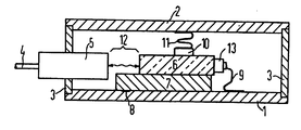
- This figure shows a housing consisting of the base 1, the side walls 3 and the cover 2 for an optoelectronic circuit module of an optical fiber communication system.
- This housing has e.g. outside dimensions 25mm x 15mm x 8.5mm.
- the length of the light path 12 is shown very large in the figure, but it can also be extremely small, e.g. be only a few pm or even much less, cf. e.g. the light path in DE-OS 33 37 131.
- the length of the light path is defined by the mutual position of the optical components 4, 6 which delimit it, in the example shown the first optical component 4 being the end of the glass fiber 4 in its connector 5 and wherein the second optical component 6, for example by an optoelectronic semiconductor diode 6, e.g. is formed by an infrared light emitting diode 6, cf. again the DE-OS 33 37 131.
- the mutual position of the two optical components 4.6 determined by their mutual. Adjustment of the length and the direction of the light path 12 in the housing 1, 2, 3.
- This adjustment of the light path must sometimes adhere to very tight tolerances, cf. e.g. again the DE-OS 33 37 131. This adjustment not only has the often very small tolerance in the axial direction. Glass fiber4, but often also a particularly low tolerance in the radial direction or glass fiber 4.
- the base 7 of the second optical component 6 shown schematically in the figure - the base 7 represents a holder for the second optical component 7 and adjoins a large area the floor 1 and was originally also rigidly connected to the floor 1 over a large area - only a small, largely punctiform point 8 was welded to the floor 1.
- the area of the point 8 had, for example, only a few% of the size which the base area of the base 7 facing the floor 1 and adjacent to the floor 1 had.
- those internal mechanical stresses on the bottom 1 were largely avoided, which with strong temperature fluctuations due to the very different linear coefficients of thermal expansion of the materials of the Bottom 1 and the base 7 occur.
- the first optical component is somehow attached to the housing, that is to say its first Bracket 5, if not inside the housing 1, 2, 3, is then attached to at least one of the housing walls 3.
- the second holder 7, which holds the second optical component 6, is attached to a section of the housing inside the housing, cf. in the figure the relevant section on the inner surface of the floor 1. Both the material on the relevant section, cf.
- the bottom 1, as well as at least the part of the second holder 7 adjoining this section, is each made of materials that can be welded to one another, the material of the section, cf. 1, has a very different linear coefficient of thermal expansion, based on the other material of the second holder 7.
- a strong temperature fluctuation is required, e.g. when used in a gas fiber communication system, which must be absolutely reliable even under extreme temperature conditions: from extreme cold, e.g. -60 ° C or -40 ° C to very high operating temperatures inside the housing of e.g. 800C or even far above it, e.g. 130 ° C.
- Such strong heating occurs, for example, in the operation of such a circuit module of a glass fiber communication system, because in the interior of the housing 1, 2, 3 an electronic component, for example an optoelectronic component - for example an infrared light-emitting diode and / or a preamplifier (for example a Semiconductor driver chip) is attached.
- an electronic component for example an optoelectronic component - for example an infrared light-emitting diode and / or a preamplifier (for example a Semiconductor driver chip) is attached.
- Such electro African components often emit very high, sometimes strongly changing heat losses during operation, which is often a relatively very strong heating of the often particularly small housing.
- housings 1, 2, 3 of optoelectronic circuit modules of a glass fiber communication system are very difficult to adequately cool on the outside, because an extremely large number of such housings 1, 2, 3 can be accommodated in very tight spaces in large closets, so that the supply of cooling air is difficult and moreover, the total heat loss to be dissipated from all housings 1, 2, 3 via the cooling air is extremely large.
- the housings should also ensure extremely large temperature fluctuations with extreme reliability and long-term stability without any interference in communications.
- the invention thus also allows extremely tight tolerances of the adjustment of the light path 12 to be observed even under such very difficult operating conditions, by the second holder 7 adjoining the relatively large section of the housing, here the bottom 1, under the aforementioned conditions, but nevertheless only via one , compared to this large section, relatively small, largely punctiform point 8 of this section is welded.
- Such spot welding on only a very small part of the area of the overall relatively large area of the section can be produced in various ways.
- emboss a knob before welding which represents a slight elevation in the interior of the housing, after which the flat base surface of the holder 7 is pressed onto the housing base 1 and welded at 8.
- This varnish has the effect that the welding can only be produced at the small point 8 with a very low rejection rate.
- a small piece of metal for example a sheet metal strip, or, for example, a small piece of wire can be attached to this point 8 between the base 1 and the holder 7 at this point 8
- Additional metal parts between the section of the housing and the holder 7 similar to the aforementioned elevations during welding cause the spot welding to occur precisely at this point 8 during spot welding.
- the section of the housing adjoining the second holder 7 does not necessarily have to be a section of the bottom 1 of the housing. Instead, it can also be another component of the housing, for example the cover 2 or a side wall 3 of the housing. It can also be, for example, an additional platform in the interior of the housing, which in turn is directly or indirectly attached to an external component 1, 2, 3 of the housing.
- both brackets 5, 7 of the two optical components 4, 6 can each be rigidly connected to one another via further mechanical components without losing the advantage according to the invention of avoiding the internal mechanical stresses in the event of temperature fluctuations.
- the invention is therefore advantageously not tied to a very special structure inside the housing 1, 2, 3.
- the relevant internal stresses can also be avoided in the case of large temperature fluctuations if the brackets 5,7, taken in practice, have practically any shape or construction.
- the invention therefore has a correspondingly large field of application.
- each of the various parts, cf. 4,5,3,1,7,6 in the figure, can consist of completely different materials, each of which have completely different linear thermal expansion coefficients. At any temperature, each of these different parts 4, 5, 3, 7, 6 acts independently on the light path 12, and not only in the longitudinal direction, ie. in the example shown in the direction of the axis of the glass fiber 4, but also perpendicular to it, that is to say radially to the glass fiber 4.
- the axis of the glass fiber 4 is parallel to the surface of the section on the Bo the 1, in which the position 8 is: Ber. Temperature fluctuations can then be minimized due to the different coefficients of thermal expansion by skillful choice of location 8, the misalignment of the light path 12.
- the misalignment of the light path 12 can be eliminated even better if the direction of the light path 12, that is to say in the example shown the direction of the axis of the glass fiber 4, is no longer selected parallel to the surface of the section, but rather in an optimal manner obliquely thereto, specifically with such a slope that with an appropriate choice of the position of the point 8, both the axial and the radial misalignments of the light path 12 are minimized.
- the invention is therefore not limited to the selection of very specific linear thermal expansion coefficients for the various components 4, 5, 3, 7, 6, that is to say it is limited to the use of a single, very special combination of materials and shapes. Therefore, the invention also allows the second optical component 6 to be made of a material which in turn has a third linear coefficient of thermal expansion which, compared to the other linear coefficients of thermal expansion, essentially the second linear coefficient of thermal expansion of its own second holder 7 is at least quite similar. Then you can namely connect the second optical component 6 rigidly over a large area to its second holder 7 without having to fear too much mechanical internal stresses at this connection between the optical component 6 and its second holder 7.
- the invention is also not restricted to very special electronic components which emit the heat loss during operation.
- these electronic see components emitting heat dissipation strongly and relatively quickly fluctuating
- the environment of the housing which is connected to this electronic component with good thermal conductivity
- the environment of the housing which is connected to this electronic component with good thermal conductivity
- the environment of the housing which is connected to this electronic component with good thermal conductivity
- the more distant parts of this housing are only subjected to very slight temperature fluctuations and, moreover, only delayed.
- the rhythmic misalignment of the light path 12 is then sometimes much greater than can be permitted.
- the first optical component 4 is the end of an optical fiber, which is generally held by a pluggable fiber optic terminal 5 as the first holder. They may even have two light paths in the housing, each of which can be attached according to the invention: namely a first light path between the end of the glass fiber 4 and a converging lens, for example a spherical lens, for sharper focusing of the light, and a second light path between them Converging lens and an optoelectronic component.
- optical components can be rigidly arranged between the light path and the optoelectronic component and optically connected upstream of the optoelectronic component: for example a quartz body or a glass body, which contains, for example, embedded glass fibers in such a way that it serves as a directional coupler, which branches into the light path leading over the glass fibers into several light path branches, for example to two optoelectronic components which are simultaneously installed in the housing interior, cf. 13 and 10 in the figure.
- a quartz body or a glass body which contains, for example, embedded glass fibers in such a way that it serves as a directional coupler, which branches into the light path leading over the glass fibers into several light path branches, for example to two optoelectronic components which are simultaneously installed in the housing interior, cf. 13 and 10 in the figure.
- one electronic component 13 can be a light-emitting diode which delivers a different light wavelength than the other light-emitting diode 10. If light-emitting diodes are fitted inside the housing, their light is generally transmitted from the housing 1, 2 via the glass fiber 4 , 3 led out. If light receiving diodes are provided in the interior of the housing, light is generally supplied to them from the outside via the glass fiber 4. Instead of two light emitting diodes 13 10, other components, for example two light receiving diodes 13, 10, can also be attached there.
Applications Claiming Priority (2)
| Application Number | Priority Date | Filing Date | Title |
|---|---|---|---|
| DE3531746 | 1985-09-05 | ||
| DE3531746 | 1985-09-05 |
Publications (1)
| Publication Number | Publication Date |
|---|---|
| EP0214464A1 true EP0214464A1 (fr) | 1987-03-18 |
Family
ID=6280218
Family Applications (1)
| Application Number | Title | Priority Date | Filing Date |
|---|---|---|---|
| EP86110752A Withdrawn EP0214464A1 (fr) | 1985-09-05 | 1986-08-04 | Boîtier pour un module de circuit opto-électronique |
Country Status (3)
| Country | Link |
|---|---|
| US (1) | US4733932A (fr) |
| EP (1) | EP0214464A1 (fr) |
| JP (1) | JPS6260276A (fr) |
Cited By (2)
| Publication number | Priority date | Publication date | Assignee | Title |
|---|---|---|---|---|
| FR2621708A1 (fr) * | 1987-10-13 | 1989-04-14 | Thomson Csf | Photocoupleur et procede de fabrication de ce photocoupleur |
| EP0889342A1 (fr) * | 1997-07-03 | 1999-01-07 | Lucent Technologies Inc. | Reduction de stress thermique dans un module laser |
Families Citing this family (20)
| Publication number | Priority date | Publication date | Assignee | Title |
|---|---|---|---|---|
| DE3244882A1 (de) * | 1982-12-03 | 1984-06-07 | Siemens AG, 1000 Berlin und 8000 München | Sende- oder empfangsvorrichtung mit einer mittels eines traegers gehalterten diode |
| US5766912A (en) | 1986-03-17 | 1998-06-16 | Novo Nordisk A/S | Humicola lipase produced in aspergillus |
| US5536661A (en) * | 1987-03-10 | 1996-07-16 | Novo Nordisk A/S | Process for the production of protein products in aspergillus |
| US4865410A (en) * | 1988-01-25 | 1989-09-12 | E. I. Du Pont De Nemours And Company | Decoupled fiber optic feedthrough assembly |
| JPH0266504A (ja) * | 1988-08-31 | 1990-03-06 | Sumitomo Electric Ind Ltd | 光送信モジュールの製造装置 |
| US4926545A (en) * | 1989-05-17 | 1990-05-22 | At&T Bell Laboratories | Method of manufacturing optical assemblies |
| US4998792A (en) * | 1990-02-16 | 1991-03-12 | International Business Machines Corporation | Fiber optic mode conditioner |
| US5778127A (en) * | 1995-06-07 | 1998-07-07 | Gilliland; Patrick | Optical transceiver and filler composition |
| US5631991A (en) * | 1996-01-26 | 1997-05-20 | International Business Machines Corporation | Plastic optical subassemblies for light transfer between an optical fiber and an optoelectronic converter and the fabrication of such plastic optical subassemblies |
| IT1283224B1 (it) * | 1996-03-11 | 1998-04-16 | Pirelli Cavi Spa | Apparato e metodo di protezione per dispositivi in fibra ottica |
| JP3180701B2 (ja) * | 1997-02-07 | 2001-06-25 | 日本電気株式会社 | 半導体レーザ装置 |
| US6243508B1 (en) * | 1999-06-01 | 2001-06-05 | Picolight Incorporated | Electro-opto-mechanical assembly for coupling a light source or receiver to an optical waveguide |
| US6201908B1 (en) * | 1999-07-02 | 2001-03-13 | Blaze Network Products, Inc. | Optical wavelength division multiplexer/demultiplexer having preformed passively aligned optics |
| US6430061B1 (en) * | 2000-11-10 | 2002-08-06 | Yazaki North America | Self-tolerancing fiber optic transceiver shield |
| US7206518B2 (en) * | 2002-11-19 | 2007-04-17 | Bookham Technology, Plc | High speed optoelectronic subassembly and package for optical devices |
| US8353634B2 (en) * | 2003-06-06 | 2013-01-15 | Intel Corporation | Mounting a planar light wave circuit in a housing |
| GB2406212B (en) * | 2003-09-16 | 2008-04-23 | Agilent Technologies Inc | Optoelectronic component with thermoelectric temperature control |
| CN1988785A (zh) * | 2005-12-23 | 2007-06-27 | 鸿富锦精密工业(深圳)有限公司 | 散热装置 |
| JP5082970B2 (ja) * | 2008-03-25 | 2012-11-28 | 富士通株式会社 | 回路基板装置 |
| US9379819B1 (en) * | 2014-01-03 | 2016-06-28 | Google Inc. | Systems and methods for reducing temperature in an optical signal source co-packaged with a driver |
Citations (4)
| Publication number | Priority date | Publication date | Assignee | Title |
|---|---|---|---|---|
| US3029505A (en) * | 1957-10-28 | 1962-04-17 | English Electric Valve Co Ltd | Method of attaching a semi-conductor device to a heat sink |
| US4399453A (en) * | 1981-03-23 | 1983-08-16 | Motorola, Inc. | Low thermal impedance plastic package |
| EP0111264A2 (fr) * | 1982-12-03 | 1984-06-20 | Siemens Aktiengesellschaft | Appareil de transmission ou réception pour équipement opto-électrique de communication |
| DE3337131A1 (de) * | 1983-10-12 | 1985-04-25 | Siemens AG, 1000 Berlin und 8000 München | Glasfaserdurchfuehrung durch eine wandoeffnung eines gehaeuses |
Family Cites Families (2)
| Publication number | Priority date | Publication date | Assignee | Title |
|---|---|---|---|---|
| JPS5946434B2 (ja) * | 1978-01-10 | 1984-11-12 | キヤノン株式会社 | 半導体レ−ザ装置 |
| JPS57164583A (en) * | 1981-04-02 | 1982-10-09 | Toshiba Corp | Self temperature compensating luminous device |
-
1986
- 1986-08-04 EP EP86110752A patent/EP0214464A1/fr not_active Withdrawn
- 1986-08-22 US US06/899,192 patent/US4733932A/en not_active Expired - Fee Related
- 1986-09-05 JP JP61208115A patent/JPS6260276A/ja active Pending
Patent Citations (4)
| Publication number | Priority date | Publication date | Assignee | Title |
|---|---|---|---|---|
| US3029505A (en) * | 1957-10-28 | 1962-04-17 | English Electric Valve Co Ltd | Method of attaching a semi-conductor device to a heat sink |
| US4399453A (en) * | 1981-03-23 | 1983-08-16 | Motorola, Inc. | Low thermal impedance plastic package |
| EP0111264A2 (fr) * | 1982-12-03 | 1984-06-20 | Siemens Aktiengesellschaft | Appareil de transmission ou réception pour équipement opto-électrique de communication |
| DE3337131A1 (de) * | 1983-10-12 | 1985-04-25 | Siemens AG, 1000 Berlin und 8000 München | Glasfaserdurchfuehrung durch eine wandoeffnung eines gehaeuses |
Cited By (2)
| Publication number | Priority date | Publication date | Assignee | Title |
|---|---|---|---|---|
| FR2621708A1 (fr) * | 1987-10-13 | 1989-04-14 | Thomson Csf | Photocoupleur et procede de fabrication de ce photocoupleur |
| EP0889342A1 (fr) * | 1997-07-03 | 1999-01-07 | Lucent Technologies Inc. | Reduction de stress thermique dans un module laser |
Also Published As
| Publication number | Publication date |
|---|---|
| US4733932A (en) | 1988-03-29 |
| JPS6260276A (ja) | 1987-03-16 |
Similar Documents
| Publication | Publication Date | Title |
|---|---|---|
| EP0214464A1 (fr) | Boîtier pour un module de circuit opto-électronique | |
| DE60101120T2 (de) | Halbleiterlaserdiodenmodul | |
| DE19947889C2 (de) | Optoelektronisches, bidirektionales Sende- und Empfangsmodul in Leadframe-Technik | |
| DE69938556T2 (de) | Verfahren und vorrichtung zur hermetischen versiegelung von elektronischen verpackungen | |
| DE19932430C2 (de) | Opto-elektronische Baugruppe sowie Bauteil für diese Baugruppe | |
| EP1088378A2 (fr) | Ensemble boitier pour module laser | |
| EP1348143A1 (fr) | Dispositif de couplage pour le couplage optique d'un guide d'ondes optiques avec un element electro-optique | |
| DE3244867A1 (de) | Sende- und/oder empfangsvorrichtung fuer einrichtungen der elektrooptischen nachrichtenuebertragung | |
| EP1174745A2 (fr) | Module optoélectronique montable en surface | |
| WO2007028667A1 (fr) | Dispositif de mesure electro-optique | |
| EP1483609A1 (fr) | Module optoelectronique et ensemble fiche male | |
| WO2001057572A2 (fr) | Module recepteur/emetteur electro-optique et son procede de fabrication | |
| EP1435118A2 (fr) | Cadre conducteur et boitier pour un element emettant un rayonnement, element emettant un rayonnement et ensemble d'affichage et/ou d'eclairage dote d'elements emettant un rayonnement | |
| DE102013225949A1 (de) | Kraftfahrzeugscheinwerfer | |
| DE102018106504B4 (de) | Anordnung mit einem TO-Gehäuse, Verfahren zu dessen Herstellung sowie optisches Datenübertragungssystem | |
| DE10112274B4 (de) | Optoelektonisches Sendemodul und Verfahren zu dessen Herstellung | |
| DE3307669C2 (fr) | ||
| DE19947113C2 (de) | Oberflächenmontierbares faseroptisches Sende- und Empfangsbauelement mit beim Zusammenbau justierbarem Umlenkreceptacle | |
| DE19910164C2 (de) | Elektrooptisches Modul | |
| EP3577506B1 (fr) | Circuit électro-optique comprenant un guide de transmission optique, module électro-optique destiné à être intégré dans un tel circuit électro-optique et procédé de fabrication d'une interface optique d'un circuit électro-optique | |
| DE102011005014B4 (de) | Verfahren zur Herstellung einer Laservorrichtung | |
| DE102005002874B3 (de) | Optoelektronisches Bauelement mit integrierter Wellenleiter-Ankopplung für passive Justage | |
| DE102016216811A1 (de) | Optokoppler mit einer optischen Übertragungsstrecke und elektrischen Anschlüssen und elektronische Baugruppe, in der ein solcher Optokoppler eingebaut ist | |
| EP0172485B1 (fr) | Boîtier commun pour deux corps semi-conducteurs | |
| WO2004104665A1 (fr) | Module micro-optique pourvu d'un boitier moule par injection et procedes de fabrication dudit module |
Legal Events
| Date | Code | Title | Description |
|---|---|---|---|
| PUAI | Public reference made under article 153(3) epc to a published international application that has entered the european phase |
Free format text: ORIGINAL CODE: 0009012 |
|
| AK | Designated contracting states |
Kind code of ref document: A1 Designated state(s): AT BE CH DE FR GB IT LI NL SE |
|
| 17P | Request for examination filed |
Effective date: 19870407 |
|
| 17Q | First examination report despatched |
Effective date: 19890331 |
|
| STAA | Information on the status of an ep patent application or granted ep patent |
Free format text: STATUS: THE APPLICATION IS DEEMED TO BE WITHDRAWN |
|
| 18D | Application deemed to be withdrawn |
Effective date: 19900301 |
|
| REG | Reference to a national code |
Ref country code: GB Ref legal event code: 732 |
|
| RIN1 | Information on inventor provided before grant (corrected) |
Inventor name: PRUSSAS, HERBERT, DIPL.-ING. Inventor name: FRENKEL, FERDINAND, DR.-PHYS. Inventor name: RAPP, LOTHAR |