EP0210105B1 - Monolitischer Magnetkopf von langer Lebensdauer mit integrierter Spule und Verfahren für seine Herstellung - Google Patents
Monolitischer Magnetkopf von langer Lebensdauer mit integrierter Spule und Verfahren für seine Herstellung Download PDFInfo
- Publication number
- EP0210105B1 EP0210105B1 EP86401570A EP86401570A EP0210105B1 EP 0210105 B1 EP0210105 B1 EP 0210105B1 EP 86401570 A EP86401570 A EP 86401570A EP 86401570 A EP86401570 A EP 86401570A EP 0210105 B1 EP0210105 B1 EP 0210105B1
- Authority
- EP
- European Patent Office
- Prior art keywords
- magnetic
- magnetic head
- patterns
- ceramic
- stack
- Prior art date
- Legal status (The legal status is an assumption and is not a legal conclusion. Google has not performed a legal analysis and makes no representation as to the accuracy of the status listed.)
- Expired - Lifetime
Links
- 230000005291 magnetic effect Effects 0.000 title claims abstract description 52
- 238000000034 method Methods 0.000 title claims description 11
- 238000004519 manufacturing process Methods 0.000 title claims description 9
- 239000000919 ceramic Substances 0.000 claims abstract description 38
- 239000000696 magnetic material Substances 0.000 claims abstract description 10
- 239000004020 conductor Substances 0.000 claims abstract description 6
- PXHVJJICTQNCMI-UHFFFAOYSA-N Nickel Chemical compound [Ni] PXHVJJICTQNCMI-UHFFFAOYSA-N 0.000 claims description 20
- 238000001465 metallisation Methods 0.000 claims description 15
- XAGFODPZIPBFFR-UHFFFAOYSA-N aluminium Chemical compound [Al] XAGFODPZIPBFFR-UHFFFAOYSA-N 0.000 claims description 14
- XEEYBQQBJWHFJM-UHFFFAOYSA-N Iron Chemical compound [Fe] XEEYBQQBJWHFJM-UHFFFAOYSA-N 0.000 claims description 10
- RYGMFSIKBFXOCR-UHFFFAOYSA-N Copper Chemical compound [Cu] RYGMFSIKBFXOCR-UHFFFAOYSA-N 0.000 claims description 9
- 239000004411 aluminium Substances 0.000 claims description 9
- 239000000463 material Substances 0.000 claims description 9
- 229910052759 nickel Inorganic materials 0.000 claims description 9
- ZOKXTWBITQBERF-UHFFFAOYSA-N Molybdenum Chemical compound [Mo] ZOKXTWBITQBERF-UHFFFAOYSA-N 0.000 claims description 6
- BQCADISMDOOEFD-UHFFFAOYSA-N Silver Chemical compound [Ag] BQCADISMDOOEFD-UHFFFAOYSA-N 0.000 claims description 6
- 229910045601 alloy Inorganic materials 0.000 claims description 6
- 239000000956 alloy Substances 0.000 claims description 6
- 230000015572 biosynthetic process Effects 0.000 claims description 6
- 239000010941 cobalt Substances 0.000 claims description 6
- GUTLYIVDDKVIGB-UHFFFAOYSA-N cobalt atom Chemical compound [Co] GUTLYIVDDKVIGB-UHFFFAOYSA-N 0.000 claims description 6
- 239000010949 copper Substances 0.000 claims description 6
- 229910017052 cobalt Inorganic materials 0.000 claims description 5
- 229910052802 copper Inorganic materials 0.000 claims description 5
- 229910052878 cordierite Inorganic materials 0.000 claims description 5
- JSKIRARMQDRGJZ-UHFFFAOYSA-N dimagnesium dioxido-bis[(1-oxido-3-oxo-2,4,6,8,9-pentaoxa-1,3-disila-5,7-dialuminabicyclo[3.3.1]nonan-7-yl)oxy]silane Chemical compound [Mg++].[Mg++].[O-][Si]([O-])(O[Al]1O[Al]2O[Si](=O)O[Si]([O-])(O1)O2)O[Al]1O[Al]2O[Si](=O)O[Si]([O-])(O1)O2 JSKIRARMQDRGJZ-UHFFFAOYSA-N 0.000 claims description 5
- 229910052742 iron Inorganic materials 0.000 claims description 5
- 239000011733 molybdenum Substances 0.000 claims description 5
- 229910052709 silver Inorganic materials 0.000 claims description 4
- 239000004332 silver Substances 0.000 claims description 4
- 229910010293 ceramic material Inorganic materials 0.000 claims description 3
- 230000006835 compression Effects 0.000 claims description 3
- 238000007906 compression Methods 0.000 claims description 3
- 230000005294 ferromagnetic effect Effects 0.000 claims description 3
- 229910001004 magnetic alloy Inorganic materials 0.000 claims description 3
- 239000011368 organic material Substances 0.000 claims description 3
- 229910000531 Co alloy Inorganic materials 0.000 claims description 2
- 238000000151 deposition Methods 0.000 claims description 2
- 230000008021 deposition Effects 0.000 claims description 2
- 230000008030 elimination Effects 0.000 claims description 2
- 238000003379 elimination reaction Methods 0.000 claims description 2
- 239000002344 surface layer Substances 0.000 claims description 2
- 229910000838 Al alloy Inorganic materials 0.000 claims 1
- 229910000881 Cu alloy Inorganic materials 0.000 claims 1
- 229910001182 Mo alloy Inorganic materials 0.000 claims 1
- 229910000990 Ni alloy Inorganic materials 0.000 claims 1
- WPBNNNQJVZRUHP-UHFFFAOYSA-L manganese(2+);methyl n-[[2-(methoxycarbonylcarbamothioylamino)phenyl]carbamothioyl]carbamate;n-[2-(sulfidocarbothioylamino)ethyl]carbamodithioate Chemical compound [Mn+2].[S-]C(=S)NCCNC([S-])=S.COC(=O)NC(=S)NC1=CC=CC=C1NC(=S)NC(=O)OC WPBNNNQJVZRUHP-UHFFFAOYSA-L 0.000 claims 1
- 239000000243 solution Substances 0.000 description 20
- 229910052782 aluminium Inorganic materials 0.000 description 17
- 239000000843 powder Substances 0.000 description 16
- LFQSCWFLJHTTHZ-UHFFFAOYSA-N Ethanol Chemical compound CCO LFQSCWFLJHTTHZ-UHFFFAOYSA-N 0.000 description 15
- 235000019441 ethanol Nutrition 0.000 description 14
- 239000002184 metal Substances 0.000 description 14
- 238000005245 sintering Methods 0.000 description 14
- 229910052751 metal Inorganic materials 0.000 description 13
- MHAJPDPJQMAIIY-UHFFFAOYSA-N Hydrogen peroxide Chemical compound OO MHAJPDPJQMAIIY-UHFFFAOYSA-N 0.000 description 12
- -1 maganese Chemical compound 0.000 description 9
- 150000003839 salts Chemical class 0.000 description 9
- 239000002904 solvent Substances 0.000 description 9
- QTBSBXVTEAMEQO-UHFFFAOYSA-N Acetic acid Chemical compound CC(O)=O QTBSBXVTEAMEQO-UHFFFAOYSA-N 0.000 description 8
- 238000007650 screen-printing Methods 0.000 description 8
- 230000007062 hydrolysis Effects 0.000 description 7
- 238000006460 hydrolysis reaction Methods 0.000 description 7
- XLYOFNOQVPJJNP-UHFFFAOYSA-N water Substances O XLYOFNOQVPJJNP-UHFFFAOYSA-N 0.000 description 7
- LYCAIKOWRPUZTN-UHFFFAOYSA-N Ethylene glycol Chemical compound OCCO LYCAIKOWRPUZTN-UHFFFAOYSA-N 0.000 description 6
- OAKJQQAXSVQMHS-UHFFFAOYSA-N Hydrazine Chemical compound NN OAKJQQAXSVQMHS-UHFFFAOYSA-N 0.000 description 6
- 150000002148 esters Chemical class 0.000 description 6
- 150000004703 alkoxides Chemical class 0.000 description 5
- 239000002585 base Substances 0.000 description 5
- 238000010438 heat treatment Methods 0.000 description 5
- 239000011777 magnesium Substances 0.000 description 5
- 150000002739 metals Chemical class 0.000 description 5
- 238000002360 preparation method Methods 0.000 description 5
- 229910052710 silicon Inorganic materials 0.000 description 5
- 229910000859 α-Fe Inorganic materials 0.000 description 5
- 239000002253 acid Substances 0.000 description 4
- 230000001476 alcoholic effect Effects 0.000 description 4
- 239000000470 constituent Substances 0.000 description 4
- 239000010410 layer Substances 0.000 description 4
- 229910052750 molybdenum Inorganic materials 0.000 description 4
- 239000010703 silicon Substances 0.000 description 4
- VEXZGXHMUGYJMC-UHFFFAOYSA-N Hydrochloric acid Chemical compound Cl VEXZGXHMUGYJMC-UHFFFAOYSA-N 0.000 description 3
- FYYHWMGAXLPEAU-UHFFFAOYSA-N Magnesium Chemical compound [Mg] FYYHWMGAXLPEAU-UHFFFAOYSA-N 0.000 description 3
- 229910002651 NO3 Inorganic materials 0.000 description 3
- NHNBFGGVMKEFGY-UHFFFAOYSA-N Nitrate Chemical compound [O-][N+]([O-])=O NHNBFGGVMKEFGY-UHFFFAOYSA-N 0.000 description 3
- XUIMIQQOPSSXEZ-UHFFFAOYSA-N Silicon Chemical compound [Si] XUIMIQQOPSSXEZ-UHFFFAOYSA-N 0.000 description 3
- VSCWAEJMTAWNJL-UHFFFAOYSA-K aluminium trichloride Chemical compound Cl[Al](Cl)Cl VSCWAEJMTAWNJL-UHFFFAOYSA-K 0.000 description 3
- 239000003795 chemical substances by application Substances 0.000 description 3
- 229940082150 encore Drugs 0.000 description 3
- 229910052749 magnesium Inorganic materials 0.000 description 3
- UEGPKNKPLBYCNK-UHFFFAOYSA-L magnesium acetate Chemical compound [Mg+2].CC([O-])=O.CC([O-])=O UEGPKNKPLBYCNK-UHFFFAOYSA-L 0.000 description 3
- 239000011654 magnesium acetate Substances 0.000 description 3
- 229940069446 magnesium acetate Drugs 0.000 description 3
- 235000011285 magnesium acetate Nutrition 0.000 description 3
- DOIRQSBPFJWKBE-UHFFFAOYSA-N phthalic acid di-n-butyl ester Natural products CCCCOC(=O)C1=CC=CC=C1C(=O)OCCCC DOIRQSBPFJWKBE-UHFFFAOYSA-N 0.000 description 3
- 239000000049 pigment Substances 0.000 description 3
- 238000004804 winding Methods 0.000 description 3
- NWZSZGALRFJKBT-KNIFDHDWSA-N (2s)-2,6-diaminohexanoic acid;(2s)-2-hydroxybutanedioic acid Chemical compound OC(=O)[C@@H](O)CC(O)=O.NCCCC[C@H](N)C(O)=O NWZSZGALRFJKBT-KNIFDHDWSA-N 0.000 description 2
- BNGXYYYYKUGPPF-UHFFFAOYSA-M (3-methylphenyl)methyl-triphenylphosphanium;chloride Chemical compound [Cl-].CC1=CC=CC(C[P+](C=2C=CC=CC=2)(C=2C=CC=CC=2)C=2C=CC=CC=2)=C1 BNGXYYYYKUGPPF-UHFFFAOYSA-M 0.000 description 2
- ZNQVEEAIQZEUHB-UHFFFAOYSA-N 2-ethoxyethanol Chemical compound CCOCCO ZNQVEEAIQZEUHB-UHFFFAOYSA-N 0.000 description 2
- QGZKDVFQNNGYKY-UHFFFAOYSA-N Ammonia Chemical compound N QGZKDVFQNNGYKY-UHFFFAOYSA-N 0.000 description 2
- KFZMGEQAYNKOFK-UHFFFAOYSA-N Isopropanol Chemical compound CC(C)O KFZMGEQAYNKOFK-UHFFFAOYSA-N 0.000 description 2
- TWRXJAOTZQYOKJ-UHFFFAOYSA-L Magnesium chloride Chemical compound [Mg+2].[Cl-].[Cl-] TWRXJAOTZQYOKJ-UHFFFAOYSA-L 0.000 description 2
- ZWEHNKRNPOVVGH-UHFFFAOYSA-N Methyl ethyl ketone Natural products CCC(C)=O ZWEHNKRNPOVVGH-UHFFFAOYSA-N 0.000 description 2
- BPQQTUXANYXVAA-UHFFFAOYSA-N Orthosilicate Chemical compound [O-][Si]([O-])([O-])[O-] BPQQTUXANYXVAA-UHFFFAOYSA-N 0.000 description 2
- 229910004298 SiO 2 Inorganic materials 0.000 description 2
- 239000000654 additive Substances 0.000 description 2
- WPYMKLBDIGXBTP-UHFFFAOYSA-N benzoic acid Chemical compound OC(=O)C1=CC=CC=C1 WPYMKLBDIGXBTP-UHFFFAOYSA-N 0.000 description 2
- 239000011230 binding agent Substances 0.000 description 2
- 238000009792 diffusion process Methods 0.000 description 2
- 238000001035 drying Methods 0.000 description 2
- IKDUDTNKRLTJSI-UHFFFAOYSA-N hydrazine monohydrate Substances O.NN IKDUDTNKRLTJSI-UHFFFAOYSA-N 0.000 description 2
- 229910052500 inorganic mineral Inorganic materials 0.000 description 2
- 150000002500 ions Chemical class 0.000 description 2
- 238000003754 machining Methods 0.000 description 2
- HQKMJHAJHXVSDF-UHFFFAOYSA-L magnesium stearate Chemical compound [Mg+2].CCCCCCCCCCCCCCCCCC([O-])=O.CCCCCCCCCCCCCCCCCC([O-])=O HQKMJHAJHXVSDF-UHFFFAOYSA-L 0.000 description 2
- 239000011707 mineral Substances 0.000 description 2
- 235000010755 mineral Nutrition 0.000 description 2
- 238000002156 mixing Methods 0.000 description 2
- 239000000203 mixture Substances 0.000 description 2
- 239000004014 plasticizer Substances 0.000 description 2
- 229920002037 poly(vinyl butyral) polymer Polymers 0.000 description 2
- OGHBATFHNDZKSO-UHFFFAOYSA-N propan-2-olate Chemical compound CC(C)[O-] OGHBATFHNDZKSO-UHFFFAOYSA-N 0.000 description 2
- 150000003376 silicon Chemical class 0.000 description 2
- WFKWXMTUELFFGS-UHFFFAOYSA-N tungsten Chemical compound [W] WFKWXMTUELFFGS-UHFFFAOYSA-N 0.000 description 2
- 229910052721 tungsten Inorganic materials 0.000 description 2
- 239000010937 tungsten Substances 0.000 description 2
- UOCLXMDMGBRAIB-UHFFFAOYSA-N 1,1,1-trichloroethane Chemical compound CC(Cl)(Cl)Cl UOCLXMDMGBRAIB-UHFFFAOYSA-N 0.000 description 1
- XBIUWALDKXACEA-UHFFFAOYSA-N 3-[bis(2,4-dioxopentan-3-yl)alumanyl]pentane-2,4-dione Chemical compound CC(=O)C(C(C)=O)[Al](C(C(C)=O)C(C)=O)C(C(C)=O)C(C)=O XBIUWALDKXACEA-UHFFFAOYSA-N 0.000 description 1
- QTBSBXVTEAMEQO-UHFFFAOYSA-M Acetate Chemical compound CC([O-])=O QTBSBXVTEAMEQO-UHFFFAOYSA-M 0.000 description 1
- 229910018072 Al 2 O 3 Inorganic materials 0.000 description 1
- QGZKDVFQNNGYKY-UHFFFAOYSA-O Ammonium Chemical compound [NH4+] QGZKDVFQNNGYKY-UHFFFAOYSA-O 0.000 description 1
- ATRRKUHOCOJYRX-UHFFFAOYSA-N Ammonium bicarbonate Chemical compound [NH4+].OC([O-])=O ATRRKUHOCOJYRX-UHFFFAOYSA-N 0.000 description 1
- OKTJSMMVPCPJKN-UHFFFAOYSA-N Carbon Chemical compound [C] OKTJSMMVPCPJKN-UHFFFAOYSA-N 0.000 description 1
- VYZAMTAEIAYCRO-UHFFFAOYSA-N Chromium Chemical compound [Cr] VYZAMTAEIAYCRO-UHFFFAOYSA-N 0.000 description 1
- 229910000570 Cupronickel Inorganic materials 0.000 description 1
- RTZKZFJDLAIYFH-UHFFFAOYSA-N Diethyl ether Chemical compound CCOCC RTZKZFJDLAIYFH-UHFFFAOYSA-N 0.000 description 1
- SXRSQZLOMIGNAQ-UHFFFAOYSA-N Glutaraldehyde Chemical compound O=CCCCC=O SXRSQZLOMIGNAQ-UHFFFAOYSA-N 0.000 description 1
- AVXURJPOCDRRFD-UHFFFAOYSA-N Hydroxylamine Chemical compound ON AVXURJPOCDRRFD-UHFFFAOYSA-N 0.000 description 1
- 229910001252 Pd alloy Inorganic materials 0.000 description 1
- 239000002202 Polyethylene glycol Substances 0.000 description 1
- 239000004372 Polyvinyl alcohol Substances 0.000 description 1
- XBDQKXXYIPTUBI-UHFFFAOYSA-M Propionate Chemical compound CCC([O-])=O XBDQKXXYIPTUBI-UHFFFAOYSA-M 0.000 description 1
- 229910020413 SiO2—MgO Inorganic materials 0.000 description 1
- 229910001035 Soft ferrite Inorganic materials 0.000 description 1
- BOTDANWDWHJENH-UHFFFAOYSA-N Tetraethyl orthosilicate Chemical compound CCO[Si](OCC)(OCC)OCC BOTDANWDWHJENH-UHFFFAOYSA-N 0.000 description 1
- XSTXAVWGXDQKEL-UHFFFAOYSA-N Trichloroethylene Chemical group ClC=C(Cl)Cl XSTXAVWGXDQKEL-UHFFFAOYSA-N 0.000 description 1
- VDGMIGHRDCJLMN-UHFFFAOYSA-N [Cu].[Co].[Ni] Chemical compound [Cu].[Co].[Ni] VDGMIGHRDCJLMN-UHFFFAOYSA-N 0.000 description 1
- HDYRYUINDGQKMC-UHFFFAOYSA-M acetyloxyaluminum;dihydrate Chemical compound O.O.CC(=O)O[Al] HDYRYUINDGQKMC-UHFFFAOYSA-M 0.000 description 1
- 238000013019 agitation Methods 0.000 description 1
- AZDRQVAHHNSJOQ-UHFFFAOYSA-N alumane Chemical class [AlH3] AZDRQVAHHNSJOQ-UHFFFAOYSA-N 0.000 description 1
- PNEYBMLMFCGWSK-UHFFFAOYSA-N aluminium oxide Inorganic materials [O-2].[O-2].[O-2].[Al+3].[Al+3] PNEYBMLMFCGWSK-UHFFFAOYSA-N 0.000 description 1
- CEGOLXSVJUTHNZ-UHFFFAOYSA-K aluminium tristearate Chemical compound [Al+3].CCCCCCCCCCCCCCCCCC([O-])=O.CCCCCCCCCCCCCCCCCC([O-])=O.CCCCCCCCCCCCCCCCCC([O-])=O CEGOLXSVJUTHNZ-UHFFFAOYSA-K 0.000 description 1
- 229940009827 aluminum acetate Drugs 0.000 description 1
- 229940063655 aluminum stearate Drugs 0.000 description 1
- CSJKPFQJIDMSGF-UHFFFAOYSA-K aluminum;tribenzoate Chemical compound [Al+3].[O-]C(=O)C1=CC=CC=C1.[O-]C(=O)C1=CC=CC=C1.[O-]C(=O)C1=CC=CC=C1 CSJKPFQJIDMSGF-UHFFFAOYSA-K 0.000 description 1
- 229910021529 ammonia Inorganic materials 0.000 description 1
- BVCZEBOGSOYJJT-UHFFFAOYSA-N ammonium carbamate Chemical compound [NH4+].NC([O-])=O BVCZEBOGSOYJJT-UHFFFAOYSA-N 0.000 description 1
- 239000001099 ammonium carbonate Substances 0.000 description 1
- 235000012501 ammonium carbonate Nutrition 0.000 description 1
- 150000003863 ammonium salts Chemical class 0.000 description 1
- 230000005587 bubbling Effects 0.000 description 1
- 238000001354 calcination Methods 0.000 description 1
- 239000000378 calcium silicate Substances 0.000 description 1
- 229910052918 calcium silicate Inorganic materials 0.000 description 1
- OYACROKNLOSFPA-UHFFFAOYSA-N calcium;dioxido(oxo)silane Chemical compound [Ca+2].[O-][Si]([O-])=O OYACROKNLOSFPA-UHFFFAOYSA-N 0.000 description 1
- 229910052799 carbon Inorganic materials 0.000 description 1
- KXDHJXZQYSOELW-UHFFFAOYSA-N carbonic acid monoamide Natural products NC(O)=O KXDHJXZQYSOELW-UHFFFAOYSA-N 0.000 description 1
- 229910052804 chromium Inorganic materials 0.000 description 1
- 239000011651 chromium Substances 0.000 description 1
- 230000001143 conditioned effect Effects 0.000 description 1
- 238000007796 conventional method Methods 0.000 description 1
- YOCUPQPZWBBYIX-UHFFFAOYSA-N copper nickel Chemical compound [Ni].[Cu] YOCUPQPZWBBYIX-UHFFFAOYSA-N 0.000 description 1
- 238000005520 cutting process Methods 0.000 description 1
- 230000003247 decreasing effect Effects 0.000 description 1
- 238000010586 diagram Methods 0.000 description 1
- 229960002380 dibutyl phthalate Drugs 0.000 description 1
- 239000002270 dispersing agent Substances 0.000 description 1
- 238000005553 drilling Methods 0.000 description 1
- HHFAWKCIHAUFRX-UHFFFAOYSA-N ethoxide Chemical compound CC[O-] HHFAWKCIHAUFRX-UHFFFAOYSA-N 0.000 description 1
- 239000000945 filler Substances 0.000 description 1
- 238000001914 filtration Methods 0.000 description 1
- 229960000587 glutaral Drugs 0.000 description 1
- 230000005484 gravity Effects 0.000 description 1
- 238000000227 grinding Methods 0.000 description 1
- 239000012456 homogeneous solution Substances 0.000 description 1
- 230000036571 hydration Effects 0.000 description 1
- 238000006703 hydration reaction Methods 0.000 description 1
- 230000003301 hydrolyzing effect Effects 0.000 description 1
- 238000005304 joining Methods 0.000 description 1
- 229910001629 magnesium chloride Inorganic materials 0.000 description 1
- 159000000003 magnesium salts Chemical class 0.000 description 1
- 235000019359 magnesium stearate Nutrition 0.000 description 1
- 239000011159 matrix material Substances 0.000 description 1
- 229910001092 metal group alloy Inorganic materials 0.000 description 1
- 239000011259 mixed solution Substances 0.000 description 1
- 229940049964 oleate Drugs 0.000 description 1
- ZQPPMHVWECSIRJ-KTKRTIGZSA-N oleic acid Chemical compound CCCCCCCC\C=C/CCCCCCCC(O)=O ZQPPMHVWECSIRJ-KTKRTIGZSA-N 0.000 description 1
- 239000005416 organic matter Substances 0.000 description 1
- 239000003960 organic solvent Substances 0.000 description 1
- SWELZOZIOHGSPA-UHFFFAOYSA-N palladium silver Chemical compound [Pd].[Ag] SWELZOZIOHGSPA-UHFFFAOYSA-N 0.000 description 1
- 229920001223 polyethylene glycol Polymers 0.000 description 1
- 229920002451 polyvinyl alcohol Polymers 0.000 description 1
- IKNCGYCHMGNBCP-UHFFFAOYSA-N propan-1-olate Chemical compound CCC[O-] IKNCGYCHMGNBCP-UHFFFAOYSA-N 0.000 description 1
- 239000011253 protective coating Substances 0.000 description 1
- 238000000197 pyrolysis Methods 0.000 description 1
- 125000001453 quaternary ammonium group Chemical group 0.000 description 1
- 230000005855 radiation Effects 0.000 description 1
- 229910000753 refractory alloy Inorganic materials 0.000 description 1
- 238000007493 shaping process Methods 0.000 description 1
- 239000007779 soft material Substances 0.000 description 1
- 239000007858 starting material Substances 0.000 description 1
- 238000003756 stirring Methods 0.000 description 1
- 239000000725 suspension Substances 0.000 description 1
- UQMOLLPKNHFRAC-UHFFFAOYSA-N tetrabutyl silicate Chemical compound CCCCO[Si](OCCCC)(OCCCC)OCCCC UQMOLLPKNHFRAC-UHFFFAOYSA-N 0.000 description 1
- WOZZOSDBXABUFO-UHFFFAOYSA-N tri(butan-2-yloxy)alumane Chemical compound [Al+3].CCC(C)[O-].CCC(C)[O-].CCC(C)[O-] WOZZOSDBXABUFO-UHFFFAOYSA-N 0.000 description 1
- YZVRVDPMGYFCGL-UHFFFAOYSA-N triacetyloxysilyl acetate Chemical compound CC(=O)O[Si](OC(C)=O)(OC(C)=O)OC(C)=O YZVRVDPMGYFCGL-UHFFFAOYSA-N 0.000 description 1
- OBROYCQXICMORW-UHFFFAOYSA-N tripropoxyalumane Chemical compound [Al+3].CCC[O-].CCC[O-].CCC[O-] OBROYCQXICMORW-UHFFFAOYSA-N 0.000 description 1
- 238000005406 washing Methods 0.000 description 1
- 239000000080 wetting agent Substances 0.000 description 1
- 239000002023 wood Substances 0.000 description 1
Images
Classifications
-
- G—PHYSICS
- G11—INFORMATION STORAGE
- G11B—INFORMATION STORAGE BASED ON RELATIVE MOVEMENT BETWEEN RECORD CARRIER AND TRANSDUCER
- G11B5/00—Recording by magnetisation or demagnetisation of a record carrier; Reproducing by magnetic means; Record carriers therefor
- G11B5/127—Structure or manufacture of heads, e.g. inductive
- G11B5/17—Construction or disposition of windings
-
- G—PHYSICS
- G11—INFORMATION STORAGE
- G11B—INFORMATION STORAGE BASED ON RELATIVE MOVEMENT BETWEEN RECORD CARRIER AND TRANSDUCER
- G11B5/00—Recording by magnetisation or demagnetisation of a record carrier; Reproducing by magnetic means; Record carriers therefor
- G11B5/10—Structure or manufacture of housings or shields for heads
-
- G—PHYSICS
- G11—INFORMATION STORAGE
- G11B—INFORMATION STORAGE BASED ON RELATIVE MOVEMENT BETWEEN RECORD CARRIER AND TRANSDUCER
- G11B5/00—Recording by magnetisation or demagnetisation of a record carrier; Reproducing by magnetic means; Record carriers therefor
- G11B5/127—Structure or manufacture of heads, e.g. inductive
- G11B5/1272—Assembling or shaping of elements
-
- G—PHYSICS
- G11—INFORMATION STORAGE
- G11B—INFORMATION STORAGE BASED ON RELATIVE MOVEMENT BETWEEN RECORD CARRIER AND TRANSDUCER
- G11B5/00—Recording by magnetisation or demagnetisation of a record carrier; Reproducing by magnetic means; Record carriers therefor
- G11B5/127—Structure or manufacture of heads, e.g. inductive
- G11B5/147—Structure or manufacture of heads, e.g. inductive with cores being composed of metal sheets, i.e. laminated cores with cores composed of isolated magnetic layers, e.g. sheets
- G11B5/1475—Assembling or shaping of elements
Definitions
- the present invention relates to magnetic heads, single or multiple, for reading or writing.
- the general structure of such a head comprises a region of magnetic material of generally annular shape with air gap, and at least one solenoid surrounding this annular region.
- the region of magnetic material is either made of a block of ferrite or of stamped or engraved metal sheets, the metal chosen being an appropriate magnetic alloy, such as the alloy known as " mumetal ".
- the magnetic field generating or receiving member consists of one or more coils of wire produced on an insulating carcass.
- the ring of magnetic material is generally produced in the form of two initially separate pieces, which are then joined after the windings have been put in place.
- All of the various parts constituting the magnetic head are housed and maintained in a housing ensuring protection and attachment to the device using the head.
- the patent of the United States of America n ° 3 731 005 describes a magnetic head in accordance with the preamble in which the magnetic head is formed from a sintered stack of ceramic sheets, at least some of which carry magnetic patterns and possibly pre-established conductive patterns, the different magnetic patterns being superimposed and being each of general annular shape with air gap.
- the laminated structure alternating the magnetic layers and the ceramic layers provides a hardness equivalent to that of ceramic, therefore much higher than that of the materials used until now.
- An object of the invention is to produce, in a monolithic assembly, the head with its magnetic region and the integrated solenoid, so as to eliminate any winding and assembly operation of elements produced separately.
- the conductors of the solenoid are formed by metallized vias formed perpendicular to the stack on either side of the magnetic patterns and distributed over at least one row along these, the different vias being joined together to form the turns of the solenoid by conductive tracks formed in the vicinity of the lower surface and the upper surface of the stack.
- the sintering in a single operation of all the constituent elements makes it possible to avoid any subsequent assembly operation and makes it possible to immediately obtain a component ensuring the same functions than the heads of the prior art, with an additional possibility of optimizing the geometry thereof, due to the absence of machining and assembly constraints.
- the sheets carry, around each via hole, a conductive flange, the different flanges of the same via being joined by the metallization of the inner wall thereof.
- the conductive tracks joining the different vias are produced in the form of buried conductors distributed over a plurality of interconnection levels.
- the air gap can possibly be formed by a saw cut made on the sintered block, the gap being filled with a non-ferromagnetic vitrifiable material.
- the step of screen printing the magnetic pattern is replaced by the deposition of a homologous pattern of raw ceramic on a sheet of magnetic material.
- high temperature will be understood to mean a maximum baking temperature above 1300 °, generally of the order of 1350 to 1400 ° C, and “low temperature” will mean a maximum sintering temperature below 1000 ° C , generally around 950 ° C.
- Ceramics with a low sintering temperature are already known, such as silico-aluminate type ceramics.
- the cordierite powder In order for the cordierite powder to be sinterable at low temperature, it will be prepared according to the process below.
- the step of heat treatment of the powder is preceded by a step of treatment with hydrogen peroxide at a temperature between 60 ° C and 100 ° C, then filtering of the suspension obtained.
- esters or salts soluble in alcohol or soluble in a solvent miscible with alcohol, or even in their corresponding acid are suitable for carrying out the invention.
- magnesium acetate Mg (CH 3 COO) 2 hydrated or not hydrated in anhydrous acetic acid, is used.
- esters can be used in the same way, such as benzoate, propionate, oleate, magnesium stearate.
- the mixed solution of aluminum and silicon salts is prepared in the presence of an alcohol which can for example be isopropanol.
- the hydrolysis which leads to the formation of the gel takes place at a temperature generally between 20 ° C and 80 ° C, preferably between 20 ° C and 50 ° C by a weak base, such as hydrated hydrazine NH 2 -NH 2 , H 2 0.
- a weak base such as hydrated hydrazine NH 2 -NH 2 , H 2 0.
- any weak base containing only volatile ions such as dilute ammonia, hydroxylamine, ammonium salts of weak acid (ammonium carbonate, ammonium carbamate) is suitable for carrying out this phase of the process.
- hydrazine hydrate is preferably used, because it plays the role of "equalizer” in hydrolysis kinetics. This role exerted by hydrazine hydrate on the kinetics of hydrolysis is of very particular interest when one uses as starting materials of aluminum and silicon alkoxides and magnesium acetate, which have kinetics d hydrolysis: aluminum alkoxide hydrolyzes easily, silicon alkoxide more difficult, magnesium acetate dissolves in water.
- the hydrated hydrazine makes it possible to carry out a partial or total hydrolysis of the alkoxides, thus granting the gelling rates and binding the Mg 2+ ion to the gel formed.
- the solution be completely free of water, since the slightest trace of water would cause an uncontrolled hydrolysis of the most fragile alkoxide, that is to say aluminum alkoxide. Note, however, that if the aluminum alkoxide is replaced by aluminum nitrate, the presence of small amounts of water is not a problem.
- the heat treatment to which the gel is subjected after hydrolysis is carried out at a temperature at most equal to 450 ° C, generally between 200 ° and 450 ° C, for a period at most equal to 24 h, generally between 1 and 2 hours, the temperature rise rate being for example between 50 ° C and 100 ° C / h.
- the purpose of this heat treatment is to remove most of the solvents, water and hydrazine. After this treatment, the powder obtained is slightly yellowish in color.
- the powder is optionally washed with hydrogen peroxide, preferably concentrated (20-30%) at a temperature between 60 ° C and 100 ° C.
- This hydrogen peroxide treatment aims to remove the last organic radicals that can be linked to the metals AI, Si or Mg.
- the hydrogen peroxide treatment can optionally be replaced by air bubbling at a temperature between 80 ° C and 100 ° C.
- this step of treatment with hydrogen peroxide can be omitted, if the application for which the powder is intended, is not disturbed by the presence of traces of carbon, resulting from the pyrolysis of organic materials which are not completely eliminated. by calcination during heat treatment.
- the powder after washing with hydrogen peroxide, is subjected to a new heat treatment which is carried out at a temperature between 450 ° C and 900 ° C, generally between 550 ° C and 700 ° C for a period at most equal at 6 h, generally between 30 and 120 min., in order to eliminate the water of constitution and hydration.
- the powder obtained is a relatively coarse powder which, after light grinding, gives a powder consisting of grains whose dimensions are between 0.01 u and 10 p, and is white in color.
- the proportions of the starting constituents may be slightly modified, without however leaving the area close to cordierite, defined by the following proportions: 60-50% Si0 2 , 5-20% MgO, 20-40% AI 2 0 3 .
- a slip is prepared by mixing approximately 1 part of powder and 1.5 parts of an organic binder (parts by weight).
- Raw ceramic sheets are then produced by pouring this slip, then drying the sheets to allow the solvent to evaporate and cut to the desired dimensions.
- the sheets thus cast are indexed by drilling holes at the periphery; these holes will serve as benchmarks for the precise superposition of the different sheets of the stack.
- the sheet thus prepared is mounted on a metal frame which will serve as position references for the rest of the operations.
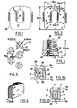
- a collar 21 is then screen printed around the vias (FIG. 3) using a paste based on conductive metal, the metallic pigment being for example a copper-nickel alloy at 90% -10%, or a silver-palladium alloy. at least 80% silver.
- the dimensions of the flanges are for example those indicated in FIG. 3, that is to say a flange with a diameter of 500 ⁇ m for a via with a diameter of 250 ⁇ m, the minimum distance between adjacent flanges being 250 ⁇ m; alternatively, it is possible to reduce these dimensions by half to further increase the compactness of the assembly (in particular if it is desired to multiply the number of rows of vias).
- the ink is then dried, for example by exposure to infrared radiation for a few tens of seconds.
- a second identically prepared sheet is then superimposed on this first sheet, provided with screen-printed vias.
- the respective thicknesses of the two types of patterns will be chosen with values as close as possible to each other.
- the metallic pigment of the ink of the magnetic pattern it is possible for example to use an alloy, close to the metal, containing by weight 75% of nickel, 5% of copper, 2% of chromium, 4% of molybdenum and 14% of iron.
- the choice of pigment must be such that its sintering temperature is compatible with that of the ceramic, and such that its constituents remain inert with respect to the latter.
- FIG. 2 gives an example of dimensioning, without limitation, of the pattern 30.
- the air gap it is possible either to provide a directly screen-printed air gap (of the order of 40 ⁇ m, value corresponding to the maximum fineness that it is possible to obtain in raw form by screen printing), or not to plan an air gap at this stage, and to form it by a saw cut on the finished block.
- the previous operation is repeated so as to add n identical layers, each provided with these two screen-printed patterns (vias and magnetic pattern), until a total thickness of the order of 1 to 5 mm is obtained (the normalized values of magnetic head thicknesses are indeed 1 mm, 3 mm and 5 mm).
- the stacking is completed by adding two sheets, identical to the two starting sheets, comprising only screen prints of vias.
- the patterns formed on the back of the stack will be produced by adding additional sheets carrying suitable patterns, before the first sheets carrying the magnetic patterns are put in place.
- FIGS. 5a and 5b schematically show a two-level interconnection N 1 , N 2 for interconnecting two series of vias, which will form the two series of turns of the solenoid; the arrows indicate the direction of the current: in the case of FIG. 5a, the interconnection is a non-planar interconnection, whereas it can be planar for the diagram of FIG. 5b.
- the vias are then metallized.
- a suitable small amount of metallization ink is deposited, which flows by gravity into the hole and is deposited on the inner wall of the via (deposit referenced 22 in FIG. 4), thus bringing together the flanges of each layer. and constituting the vertical conductive parts of each loop of the solenoid.
- the ink used is an ink of the same kind as that used for the screen printing of the flanges 21 and the conductive tracks 40, with the addition of a ceramic filler, preferably of the same type of ceramic as that used for the preparation of the sheets. dielectric.
- the sheet is then separated from its metal frame, and it is pressed into a punch-matrix assembly so as to agglomerate the stack in a homogeneous block. If bonding tracks have to be transferred to the surface of the component, this stage of the process is screen printed.
- the residual organic materials are removed, then the ceramic is sintered (for example by baking at 950 ° for 3 hours).
- the individual components of the sintered ceramic sheet are then cut (this cutting can also be done before sintering the ceramic).
- FIG. 6 shows, in perspective view, a magnetic head produced according to the teachings of the invention.
- the region of contact with the magnetic strip to be read or written consists of a laminated structure alternating magnetic material and ceramic material of great hardness, hence the long longevity of these heads.
- FIG. 6 shows, for example, a double head, therefore comprising two air gaps and two sets of solenoids.
- Alumina A1 2 0 3 is mixed with 2 to 4% by weight, preferably about 2.5%, of calcium silicate (51.8% Si0 2 and 48.2% CaO).
- the powder obtained will have a density of approximately 90 to 95% after sintering at 1400 ° C.
- the sintering must be carried out in a controlled, reducing atmosphere.
- the maximum sintering temperature will be around 1400 ° C.
Landscapes
- Engineering & Computer Science (AREA)
- Manufacturing & Machinery (AREA)
- Magnetic Heads (AREA)
- Compositions Of Oxide Ceramics (AREA)
- Slide Fasteners, Snap Fasteners, And Hook Fasteners (AREA)
- Adornments (AREA)
- Soft Magnetic Materials (AREA)
Claims (10)
Priority Applications (1)
| Application Number | Priority Date | Filing Date | Title |
|---|---|---|---|
| AT86401570T ATE58799T1 (de) | 1985-07-16 | 1986-07-15 | Monolitischer magnetkopf von langer lebensdauer mit integrierter spule und verfahren fuer seine herstellung. |
Applications Claiming Priority (2)
| Application Number | Priority Date | Filing Date | Title |
|---|---|---|---|
| FR8510870A FR2585168B1 (fr) | 1985-07-16 | 1985-07-16 | Tete magnetique longue duree monolithique a solenoide integre, et procede pour sa fabrication |
| FR8510870 | 1985-07-16 |
Publications (2)
| Publication Number | Publication Date |
|---|---|
| EP0210105A1 EP0210105A1 (de) | 1987-01-28 |
| EP0210105B1 true EP0210105B1 (de) | 1990-11-28 |
Family
ID=9321339
Family Applications (1)
| Application Number | Title | Priority Date | Filing Date |
|---|---|---|---|
| EP86401570A Expired - Lifetime EP0210105B1 (de) | 1985-07-16 | 1986-07-15 | Monolitischer Magnetkopf von langer Lebensdauer mit integrierter Spule und Verfahren für seine Herstellung |
Country Status (4)
| Country | Link |
|---|---|
| EP (1) | EP0210105B1 (de) |
| AT (1) | ATE58799T1 (de) |
| DE (1) | DE3675834D1 (de) |
| FR (1) | FR2585168B1 (de) |
Family Cites Families (7)
| Publication number | Priority date | Publication date | Assignee | Title |
|---|---|---|---|---|
| US2674659A (en) * | 1951-11-02 | 1954-04-06 | Bell Telephone Labor Inc | Magnetic head and method of making same |
| DE1043652B (de) * | 1957-04-25 | 1958-11-13 | Philips Nv | Magnetkopf und Verfahren zu dessen Herstellung |
| FR1446508A (fr) * | 1965-06-17 | 1966-07-22 | Ibm | Tête d'enregistrement magnétique |
| US3731005A (en) * | 1971-05-18 | 1973-05-01 | Metalized Ceramics Corp | Laminated coil |
| JPS56127914A (en) * | 1980-03-13 | 1981-10-07 | Tdk Corp | Electricity and magnetism converting element |
| JPS5736420A (ja) * | 1980-08-12 | 1982-02-27 | Tdk Corp | Jikihetsudo |
| JPS5740717A (en) * | 1980-08-21 | 1982-03-06 | Fujitsu Ltd | Thin magnetic head |
-
1985
- 1985-07-16 FR FR8510870A patent/FR2585168B1/fr not_active Expired
-
1986
- 1986-07-15 DE DE8686401570T patent/DE3675834D1/de not_active Expired - Lifetime
- 1986-07-15 EP EP86401570A patent/EP0210105B1/de not_active Expired - Lifetime
- 1986-07-15 AT AT86401570T patent/ATE58799T1/de not_active IP Right Cessation
Also Published As
| Publication number | Publication date |
|---|---|
| ATE58799T1 (de) | 1990-12-15 |
| EP0210105A1 (de) | 1987-01-28 |
| DE3675834D1 (de) | 1991-01-10 |
| FR2585168B1 (fr) | 1989-12-29 |
| FR2585168A1 (fr) | 1987-01-23 |
Similar Documents
| Publication | Publication Date | Title |
|---|---|---|
| EP0091072B1 (de) | Verfahren zur Einkapselung von Halbleiterbauelementen sowie derartig eingekapselte Bauelemente | |
| EP0145599B1 (de) | Aluminiumoxid-Verbindungssubstrat für elektronische Bauteile und Verfahren zur Herstellung desselben | |
| EP3371826B1 (de) | Herstellungsverfahren einer chipvorrichtung mit integriertem schaltkreis durch direkte aufbringung eines leitermaterials | |
| KR20090060296A (ko) | 반도체 기판상에 전기 접점을 생성하는 방법, 반도체 기판 및 그 방법의 사용 | |
| FR2923081A1 (fr) | Procede d'interconnexion verticale de modules electroniques 3d par des vias. | |
| EP0006810A1 (de) | Verfahren zur Herstellung einer integrierten Hybrid-Schaltung | |
| WO2014098350A1 (ko) | 코어 (Se)-쉘 (Ag2Se) 나노입자를 이용한 A(C)IGS계 박막의 제조방법, 이에 의해 제조된 A(C)IGS계 박막 및 이를 포함하는 탠덤 태양전지 | |
| EP0720776B1 (de) | Anode für einen flachen bildschirm | |
| CA2529899C (fr) | Procede de fabrication de pieces pour composants electroniques passifs et pieces obtenues | |
| EP0210105B1 (de) | Monolitischer Magnetkopf von langer Lebensdauer mit integrierter Spule und Verfahren für seine Herstellung | |
| US20050227497A1 (en) | Light transparent substrate imprint tool with light blocking distal end | |
| CN100558219C (zh) | 电子器件的制造方法 | |
| JP2000332100A (ja) | 半導体装置の製造方法および半導体装置 | |
| WO2014064278A1 (fr) | Circuit électrique, module électronique pour carte à puce réalisé sur ce circuit électrique et procédé pour la réalisation d'un tel circuit électrique | |
| JPS58502078A (ja) | 半導体装置の製造方法およびそうして得られる半導体装置 | |
| EP2368262B1 (de) | Verfahren zur kollektiven herstellung von elektronikmodulen für oberflächenanbringung | |
| EP3717679B1 (de) | Elektrische schaltung, elektronisches modul für eine auf der elektrischen schaltung geformte chipkarte und verfahren zur herstellung solch einer elektrischen schaltung | |
| EP4154309B1 (de) | Elektrische schaltung für ein elektronisches chipkartenmodul mit farbigen kontakten und verfahren zu deren herstellung | |
| EP0213989A1 (de) | Verfahren zur Herstellung eines mehrschichtigen kapazitiven Bauelements mit einem keramischen Dielektrikum des Cordierittyps sowie hergestelltes Bauelement | |
| FR2844096A1 (fr) | Procede de fabrication d'un circuit electrique comprenant une etape de polissage | |
| JPH08181029A (ja) | 電子部品の製造方法 | |
| EP3226082B1 (de) | Komponente eines uhrwerks | |
| WO2022069270A1 (fr) | Vitrage chauffant à contrôle solaire transparent aux radiofréquences | |
| JP2002212602A (ja) | 磁石材料およびその製造方法 | |
| FR3051313B1 (fr) | Procede de fabrication d’un circuit imprime, circuit imprime obtenu par ce procede et module de carte a puce comportant un tel circuit imprime |
Legal Events
| Date | Code | Title | Description |
|---|---|---|---|
| PUAI | Public reference made under article 153(3) epc to a published international application that has entered the european phase |
Free format text: ORIGINAL CODE: 0009012 |
|
| AK | Designated contracting states |
Kind code of ref document: A1 Designated state(s): AT BE CH DE GB IT LI NL SE |
|
| 17P | Request for examination filed |
Effective date: 19870706 |
|
| 17Q | First examination report despatched |
Effective date: 19890919 |
|
| GRAA | (expected) grant |
Free format text: ORIGINAL CODE: 0009210 |
|
| ITF | It: translation for a ep patent filed | ||
| AK | Designated contracting states |
Kind code of ref document: B1 Designated state(s): AT BE CH DE GB IT LI NL SE |
|
| REF | Corresponds to: |
Ref document number: 58799 Country of ref document: AT Date of ref document: 19901215 Kind code of ref document: T |
|
| GBT | Gb: translation of ep patent filed (gb section 77(6)(a)/1977) | ||
| REF | Corresponds to: |
Ref document number: 3675834 Country of ref document: DE Date of ref document: 19910110 |
|
| PLBE | No opposition filed within time limit |
Free format text: ORIGINAL CODE: 0009261 |
|
| STAA | Information on the status of an ep patent application or granted ep patent |
Free format text: STATUS: NO OPPOSITION FILED WITHIN TIME LIMIT |
|
| 26N | No opposition filed | ||
| PGFP | Annual fee paid to national office [announced via postgrant information from national office to epo] |
Ref country code: SE Payment date: 19920714 Year of fee payment: 7 |
|
| PGFP | Annual fee paid to national office [announced via postgrant information from national office to epo] |
Ref country code: NL Payment date: 19920731 Year of fee payment: 7 |
|
| PGFP | Annual fee paid to national office [announced via postgrant information from national office to epo] |
Ref country code: AT Payment date: 19920804 Year of fee payment: 7 |
|
| PGFP | Annual fee paid to national office [announced via postgrant information from national office to epo] |
Ref country code: BE Payment date: 19920807 Year of fee payment: 7 |
|
| PGFP | Annual fee paid to national office [announced via postgrant information from national office to epo] |
Ref country code: CH Payment date: 19920818 Year of fee payment: 7 |
|
| PG25 | Lapsed in a contracting state [announced via postgrant information from national office to epo] |
Ref country code: AT Effective date: 19930715 |
|
| PG25 | Lapsed in a contracting state [announced via postgrant information from national office to epo] |
Ref country code: SE Effective date: 19930716 |
|
| ITTA | It: last paid annual fee | ||
| PG25 | Lapsed in a contracting state [announced via postgrant information from national office to epo] |
Ref country code: LI Effective date: 19930731 Ref country code: CH Effective date: 19930731 Ref country code: BE Effective date: 19930731 |
|
| BERE | Be: lapsed |
Owner name: EUROFARAD-EFD Effective date: 19930731 |
|
| PG25 | Lapsed in a contracting state [announced via postgrant information from national office to epo] |
Ref country code: NL Effective date: 19940201 |
|
| NLV4 | Nl: lapsed or anulled due to non-payment of the annual fee | ||
| REG | Reference to a national code |
Ref country code: CH Ref legal event code: PL |
|
| PGFP | Annual fee paid to national office [announced via postgrant information from national office to epo] |
Ref country code: GB Payment date: 19940707 Year of fee payment: 9 |
|
| PGFP | Annual fee paid to national office [announced via postgrant information from national office to epo] |
Ref country code: DE Payment date: 19940721 Year of fee payment: 9 |
|
| EUG | Se: european patent has lapsed |
Ref document number: 86401570.6 Effective date: 19940210 |
|
| PG25 | Lapsed in a contracting state [announced via postgrant information from national office to epo] |
Ref country code: GB Effective date: 19950715 |
|
| GBPC | Gb: european patent ceased through non-payment of renewal fee |
Effective date: 19950715 |
|
| PG25 | Lapsed in a contracting state [announced via postgrant information from national office to epo] |
Ref country code: DE Effective date: 19960402 |
|
| PG25 | Lapsed in a contracting state [announced via postgrant information from national office to epo] |
Ref country code: IT Free format text: LAPSE BECAUSE OF NON-PAYMENT OF DUE FEES;WARNING: LAPSES OF ITALIAN PATENTS WITH EFFECTIVE DATE BEFORE 2007 MAY HAVE OCCURRED AT ANY TIME BEFORE 2007. THE CORRECT EFFECTIVE DATE MAY BE DIFFERENT FROM THE ONE RECORDED. Effective date: 20050715 |