EP0206462A2 - Verfahren und Schattungsanordnung zum Vorladen einer dynamischen in Kaskode geschalteten Logikschaltung - Google Patents
Verfahren und Schattungsanordnung zum Vorladen einer dynamischen in Kaskode geschalteten Logikschaltung Download PDFInfo
- Publication number
- EP0206462A2 EP0206462A2 EP86302860A EP86302860A EP0206462A2 EP 0206462 A2 EP0206462 A2 EP 0206462A2 EP 86302860 A EP86302860 A EP 86302860A EP 86302860 A EP86302860 A EP 86302860A EP 0206462 A2 EP0206462 A2 EP 0206462A2
- Authority
- EP
- European Patent Office
- Prior art keywords
- output
- node
- signal
- circuit
- level
- Prior art date
- Legal status (The legal status is an assumption and is not a legal conclusion. Google has not performed a legal analysis and makes no representation as to the accuracy of the status listed.)
- Granted
Links
Images

Classifications
-
- H—ELECTRICITY
- H03—ELECTRONIC CIRCUITRY
- H03K—PULSE TECHNIQUE
- H03K19/00—Logic circuits, i.e. having at least two inputs acting on one output; Inverting circuits
- H03K19/02—Logic circuits, i.e. having at least two inputs acting on one output; Inverting circuits using specified components
- H03K19/173—Logic circuits, i.e. having at least two inputs acting on one output; Inverting circuits using specified components using elementary logic circuits as components
- H03K19/1733—Controllable logic circuits
- H03K19/1738—Controllable logic circuits using cascode switch logic [CSL] or cascode emitter coupled logic [CECL]
Definitions
- the invention relates generally to logic circuits.
- the invention relates to a method for consistently precharging the nodes of a dynamic logic circuit.
- a recently developed technology for logic circuits is called alternatively a cascode voltage switch (CVS) or CMOS domino circuit.
- CVS cascode voltage switch
- An early description of this type of circuit appears in a technical article by Krambeck et al., entitled “HighSpeed Compact Circuits with CMOS” and appearing in IEEE Journal of Solid-State Circuits, volume SC-17, No.3, June 19, 1982 at pp 614-619.
- a similar circuit is disclosed by Booher in US-A-3,601,627.
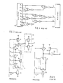
- the overall structure of a generalised but exemplary CVS circuit is shown in Figure 1.
- An input register 10 provides a plurality of primary inputs of which in this example eight Pl 1 -Pl 8 , are explicitly shown.
- logic modules f 1 -f 7 each consisting of a group of logic transistors, having one or more inputs X i and followed by an inverter.
- the inputs X; of each logic group f are either taken from the primary inputs PI, -Pl 8 or from the output of the inverter of a logic group f of a previous stage.
- Selected outputs, three Y, -Y z are shown in the example, are led to an - output register 12.
- the complemented output of a logic group f and the following inverter follow from the usual implementations of the logic group f.
- a relatively simple logic group 14 is shown in Figure 2 and is implemented with five n-channel field effect transistors 16 each having a gate input X,-X.. The function implemented is -OR(AND(X" X,, X s ), AND (X., X 4 )).
- This logic group 14 is presented for sake of example and much more complicated logic groups are possible.
- a signal node No of the logic group 14 is connected to a power supply (not shown) through an upper precharge p-channel transistor 18.
- a grounding node N g of the logic group 14 is connected to ground potential (not shown) through a lower precharge n-channel transistor 20.
- the inputs (X1-X5) are held low so that all the n-channel transistors 16 are turned OFF, that is, made non-conducting.
- a precharge signal (-PRECHARGE) applied to the gate electrodes of transistors 18 and 20 goes low, p-channel transistor 18 is turned ON and n-channel transistor 20 is turned OFF. This isolates the grounding node N G of the logic group 14 from ground potential but connects the signal node N 0 to the power supply voltage. As a result, the signal node No is charged during the precharge period to the supply voltage.
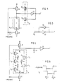
- the signal node No is further connected to the input of a CMOS inverter gate 22 consisting of a p-channel transistor 24 and an n-channel transistor 26 serially connected between the power supply voltage and ground potential of the circuits.
- the inverter input connects node No to the gate electrodes of transistors 24 and 26 and an inverter output Y is taken from the common connection between the two transistors 24 and 26. It should be noted that since at the end of the precharge period, the signal on the signal node No is high, the signal on inverter output Y is low.
- the output signal Y may be further connected as an input signal X 1 to another logic group the low level on the output Y following precharging of its input logic group is consistent with the requirement that all the input to a subsequent logic group must be at a low level during precharging of this group.
- the primary inputs Pi to the circuit from register 10 are required to follow this same convention by means of appropriate interface circuits.
- the (-PRECHARGE) signal returns to its high level and transistor 20 turns ON and transistor 18 turns OFF.
- the grounding node N G is therefore reconnected to ground but the signal node No is isolated from the power supply and left floating with the precharge.
- the primary inputs Pl, -Pl 8 from input register 10 then assume their signal values and are applied during an evaluation phase as input to the various logic modules f with the result that low impedance paths are established through some modules and not through others depending upon the levels of inputs signals Xi selectively applied thereto.
- a low impedance discharge path from the signal node No to the grounding N G is formed by an appropriate combination of input signals X, -X 5 , then the precharged voltage node No is discharged through the logic group to a low state. This new low state then switches the CMOS inverter 22 and the output signal Y goes high. If, on the other hand, no discharge path is created, then the output signal Y remains high.
- the output signal Y may be applied as an input to a logic group of a further precharged stage and, may thus cause a corresponding node of that logic group to discharge and so on through the circuit. Hence, the name domino.
- a CVS circuit is dynamic in that it required the precharging of the signal node No and the subsequent monitoring of the signal on that signal node No, to determine whether it continues to be precharged or is discharged through its associated logic group.
- a problem associated with the leakage and fluctuation of the precharge from the signal node No there is a problem associated with the leakage and fluctuation of the precharge from the signal node No.
- Leakage in a dynamic circuit is a pervasive problem and several solutions have been proposed. For example, see US-A-4,433,257 - (Kinoshita), US-A-3,989,955, US-A-4,464,587 (Suzuki) and US-A-4,398,270 (Taylor)
- a p-channel transistor 28 is connected as a feed-back device between the output and input of the inverter 22 and the power supply.
- the gate electrode of transistor 28 is connected to the output Y of the inverter 22.
- transistor 28 turns ON thus closing the feedback path and solidly connecting the signal node No to the power supply voltage.
- the feedback arrangement needs to be sufficiently weak such that when the signal node No is positively discharged, transistor 28 does not continue to feed sufficient charge to the inverter 22 to prevent its output signal Y from turning off the transistor 28.
- FIG.4 A yet more elaborate feedback is illustrated in Fig.4, in which additionally an n-channel feedback transistor 30 is connected as a feed-back device between the output and input of the inverter 22 and ground potential.
- the gate electrode of transistor 30 is connected to the output Y of the inverter 22.
- transistor 28 turns OFF
- transistor 30 turns ON and solidly connects the signal node No and the input of the inverter 22 to ground potential.
- charge fluctuations and leakage into the signal node No are compensated for.
- the n-channel feedback arrangement needs to be sufficiently weak so that its effect can be overcome by a subsequent positive charging of the signal node No.
- the feedback transistors 28 and 30 themselves comprise a weak feedback inverter 32, and are illustrated in block form in Fig.5.
- the two back-to-back inverters 22 and 32 thus act as a regenerative memory for storing any strong signal impressed upon the signal node No.
- CVS circuits have many advantages but the technology appears to be plagued with spurious signals or glitches.
- the signal on the signal node No is subject to fluctuations, particularly at the beginning of the evaluation phase.
- the feedback arrangements described above and illustrated in Figures 3 and 4 are aimed at reducing the effects of these fluctuations.
- the feedback must be weak for circuit to operate and may not be sufficient to prevent the situation arising where an output signal Y varies momentarily to an incorrect high value. Even if the feedback arrangements subsequently bring the output signal Y to the correct low value, the damage may have already been done in that the transient incorrect value may have already discharged the logic group f of a subsequent stage.
- the feedback arrangements alone are inadequate to solve the problem.
- an object of this invention is to provide a cascode voltage switching circuit that has reduced susceptibility to internal noise.
- a further object of this invention is to reduce the fluctuations without an undue increase in the complexity of the circuit.
- the invention can be summarised as a method of precharging a cascode voltage switch circuit in which the output signal resulting from the evaluation phase of the previous cycle of the circuit is maintained upon the output during the current precharge phase.
- a pass transistor between the logic gate and the output inverter is turned OFF, thus isolating the output from the precharging voltage.
- Both the signal node and the grounding node are then precharged.
- the continued application of the previously derived output signals to the logic groups during this precharging ensures that all internal capacitive nodes which had been discharged in the previous cycle are fully precharged in the current precharging period.
- the capacitance 34 is not the only parasitic capacitance in the circuits. There is additional capacitance 36, 38 and 40 at the points between the logic gates 16. However, according to the design convention for CVS circuits, all the inputs X 1 -X 5 are low during the precharging period so that the associated transistors 16,-16 s are turned off during precharging. As a result, the parasitic capacitances 36-40 within the logic group 14 are not accessible and are not precharged. For the most part, the amount of charge on the capacitances 36-40 within a logic group at the end of the precharging period is determined by the amount to which they were charged at the end of the prior evaluation period.
- This amount of charge is determined by the values of the input signals X 1 -X 5 to the current logic group which were applied in the prior evaluation period. For example, assuming that the internal capacitance 36-40 were fully charged before the prior evaluation period, then if all the input signals X,-X. were low (binary '0') in the prior evaluation period, the intemal capacitance 36-38 remain fully charged for the current evaluation period. If, on the other hand, all the input signal X,-X s in the prior evaluation period were high (binary 1), then all the internal capacitances 36-40 of the group will have been discharded. Furthermore, different combinations of input signals X,-X.
- the precharge on the signal node No that is, the precharge on the capacitance 34
- the precharge on the signal node No may be discharged to ground if the input sig- nais X,-X, turn on sufficient transistors 16 to form a conducting path to ground.
- the precharge on the signal node No is discharged to ground through the conducting path of transistors, although the transition time may depend upon the amount of charge on the intemal capacitances 36-40.
- the problem should be relatively small because all the capacitances have been charged by similar voltages.
- the precharge on the capacitance 34 is redistributed to the discharged capacitance 36 or 40 or possibly both. This redistribution of the precharge causes the voltage on the signal node No to dip. The amount of this dip is thus dependent upon the input signals X 1 -X 5 of the prior evaluation phase as well as the input signals X,-X, of the current evaluation phase, and thus is difficult to predict or control.
- the feedback around the inverter 22, as shown in either Figures 3 or 4, can compensate for this dip and bring the signal on the signal node No back up to a solid high as long as the dip is not too severe.
- the feedback must be weak so that a transient dip appears inevitable in view of the dynamic nature of a CVS circuit. It is possible that the feedback eventually brings the high signal on the signal node No back to its correct value, but, in the meantime, the output signal Y may have changed enough to have caused a logic group f of the following stage to have discharged. Once this following logic group has been discharged, the application of the correct input signals to that stage, intended to keep that logic group charged, cannot recharge the signal node No of the following group. As a result, transient signal errors become permanent by the domino nature of a CVS circuit.
- the invention uses this understanding of the problem to reduce fluctuations by the following method.
- the output signal Y is memorised and then held during a part of the precharging period at the level it had in the prior evaluation phase. That is before the current precharging period. Then whilst the value is held, both the signal node No and the ground node N ⁇ of the logic group are both precharged. Since precharging of all the logic units is conducted simultaneously, the inputs Xi to all the logic groups are held at the values of the previous evaluation phase. However, as will be seen the inputs Xi are forced to the low level before the end of the precharge phase as is required.
- a (-PRECHARGE) signal having a slightly different function than the (-PRECHARGE) of Figures 2 and 6, directly controls the gate of an n-channel pass transistor 42 connecting the signal node No to the input to the inverter 22.
- transistor 42 is turned OFF and the signal node No is isolated from the inverter 22 and the weak feedback inverter 32.
- the combination of the inverters 22 and 32 act as a memory device. With the memory device thus isolated from the precharging, the value of the output signal Y of the prior evaluation phase is held during the current precharging period. This condition applies to the output of all CVS modules.
- the (-PRECHARGE) signal is passed, as shown in Figure 8, through two inverters 44 and 46, to form a delayed precharged signal on line C2 which is applied to the upper and lower precharge transistors 18 and 20 in the usual way and additionally to a further precharge p-channel transistor 48 connected between the power supply and the grounding node N G of the logic group 14.
- the delayed low level of the (-PRECHARGE) signal turns transistor 20 OFF and transistors 18 and 48 ON.
- the signal node No having been previously isolated from the inverters 22 and 32 to which it is normally connected is then connected to the power supply via the transistor 18 for precharging.
- the grounding node N G is isolated from ground by the transistor 20 turning OFF and itself connected to the power supply for precharging via the transistor 48.
- both nodes No and N G of the logic group 14 are precharged to the supply voltage.
- the input signals X,-X N are held at their respective values of the prior evaluation phase by memory units of other logic modules corresponding to the inverters 22 and 32.
- Primary inputs to the CVS circuits must follow the same convention which could be accomplished by attaching a pass gate 42 and inverters 22 and 32 to the primary inputs Pl 1 .
- both of the nodes No and N G are held at the precharging voltage during precharging so that whatever internal capacitances 36-40 were discharged during the prior evaluation are once again precharged.
- the precharging of all capacitances is to the same supply power voltage.
- the circuit of Figure 7 shows that the delayed precharge signal on line C o is generated locally, that is, in the neighbourhood of the logic group 14, directly from the (-PRECHARGE) signal.
- This approach necessitates two additional inverters 44 and 46 for each logic group t4.
- both the precharge signal (-PRECHARGE) and the delayed version on line C o ta be generated at one poing on an integrated circuit and then both to be distributed to aff of the logic groups 14 on the integrated circuit
- This central generation of both precharging signals of course necessitates additional interconnections.
- the routing for both sets of interconnections can be the same so that the complexity is not greatly increased.
- any time skew affecting one of the precharging signal affects the other. As a result, the amount of delay At is easily maintained over the long interconnections.
Applications Claiming Priority (2)
| Application Number | Priority Date | Filing Date | Title |
|---|---|---|---|
| US726211 | 1985-04-23 | ||
| US06/726,211 US4700086A (en) | 1985-04-23 | 1985-04-23 | Consistent precharge circuit for cascode voltage switch logic |
Publications (3)
| Publication Number | Publication Date |
|---|---|
| EP0206462A2 true EP0206462A2 (de) | 1986-12-30 |
| EP0206462A3 EP0206462A3 (en) | 1988-12-14 |
| EP0206462B1 EP0206462B1 (de) | 1991-10-23 |
Family
ID=24917656
Family Applications (1)
| Application Number | Title | Priority Date | Filing Date |
|---|---|---|---|
| EP86302860A Expired - Lifetime EP0206462B1 (de) | 1985-04-23 | 1986-04-16 | Verfahren und Schattungsanordnung zum Vorladen einer dynamischen in Kaskode geschalteten Logikschaltung |
Country Status (4)
| Country | Link |
|---|---|
| US (1) | US4700086A (de) |
| EP (1) | EP0206462B1 (de) |
| JP (1) | JPS61247122A (de) |
| DE (1) | DE3682121D1 (de) |
Cited By (1)
| Publication number | Priority date | Publication date | Assignee | Title |
|---|---|---|---|---|
| EP0458766B1 (de) * | 1990-05-25 | 1997-04-16 | STMicroelectronics S.r.l. | Filterschaltung für Spitzen in logischen Signalen |
Families Citing this family (56)
| Publication number | Priority date | Publication date | Assignee | Title |
|---|---|---|---|---|
| US4936647A (en) * | 1985-05-15 | 1990-06-26 | Babcock Industries, Inc. | High tensile strength compacted towing cable with signal transmission element |
| JPS6342216A (ja) * | 1986-08-08 | 1988-02-23 | Hitachi Ltd | バイポ−ラトランジスタと電界効果トランジスタとを含む複合回路 |
| JPS6366789A (ja) * | 1986-09-09 | 1988-03-25 | Mitsubishi Electric Corp | Cmos行デコ−ダ回路 |
| US4763023A (en) * | 1987-02-17 | 1988-08-09 | Rockwell International Corporation | Clocked CMOS bus precharge circuit having level sensing |
| JPS63204815A (ja) * | 1987-02-20 | 1988-08-24 | Hitachi Ltd | 半導体論理回路 |
| JPS63228494A (ja) * | 1987-03-18 | 1988-09-22 | Fujitsu Ltd | ダイナミツク型デコ−ダ回路 |
| JPS63253718A (ja) * | 1987-04-09 | 1988-10-20 | Rohm Co Ltd | ゲ−ト回路 |
| JP2619415B2 (ja) * | 1987-09-24 | 1997-06-11 | 株式会社日立製作所 | 半導体論理回路 |
| KR910002748B1 (ko) * | 1988-04-12 | 1991-05-04 | 삼성 반도체통신 주식회사 | 반도체장치에 있어서 데이타 출력 버퍼회로 |
| US5629907A (en) * | 1991-06-18 | 1997-05-13 | Dallas Semiconductor Corporation | Low power timekeeping system |
| US4876465A (en) * | 1988-06-17 | 1989-10-24 | Dallas Semiconductor Corporation | Dynamic CMOS buffer for low current switching |
| US4857764A (en) * | 1988-06-30 | 1989-08-15 | Harris Corporation | Current compensated precharged bus |
| JPH0377129A (ja) * | 1989-08-18 | 1991-04-02 | Mitsubishi Electric Corp | プリチャージ方式バス回路 |
| JPH0793026B2 (ja) * | 1989-09-20 | 1995-10-09 | 富士通株式会社 | デコーダ回路 |
| US5329176A (en) * | 1991-04-12 | 1994-07-12 | Hewlett-Packard Company | Self-timed clocking system and method for self-timed dynamic logic circuits |
| US5389835A (en) * | 1991-04-12 | 1995-02-14 | Hewlett-Packard Company | Vector logic method and dynamic mousetrap logic gate for a self-timed monotonic logic progression |
| US5208490A (en) * | 1991-04-12 | 1993-05-04 | Hewlett-Packard Company | Functionally complete family of self-timed dynamic logic circuits |
| DE4115081A1 (de) * | 1991-05-08 | 1992-11-12 | Siemens Ag | Logikschaltung fuer asynchrone schaltungen mit n-kanal-logikblock und dazu inversem p-kanal-logikblock |
| US5189319A (en) * | 1991-10-10 | 1993-02-23 | Intel Corporation | Power reducing buffer/latch circuit |
| US5329174A (en) * | 1992-10-23 | 1994-07-12 | Xilinx, Inc. | Circuit for forcing known voltage on unconnected pads of an integrated circuit |
| US5389836A (en) * | 1993-06-04 | 1995-02-14 | International Business Machines Corporation | Branch isolation circuit for cascode voltage switch logic |
| US5528463A (en) * | 1993-07-16 | 1996-06-18 | Dallas Semiconductor Corp. | Low profile sockets and modules for surface mountable applications |
| US5579206A (en) * | 1993-07-16 | 1996-11-26 | Dallas Semiconductor Corporation | Enhanced low profile sockets and module systems |
| US5440182A (en) * | 1993-10-22 | 1995-08-08 | The Board Of Trustees Of The Leland Stanford Junior University | Dynamic logic interconnect speed-up circuit |
| US5399921A (en) * | 1993-12-14 | 1995-03-21 | Dobbelaere; Ivo J. | Dynamic complementary pass-transistor logic circuit |
| US5517136A (en) * | 1995-03-03 | 1996-05-14 | Intel Corporation | Opportunistic time-borrowing domino logic |
| US5495188A (en) * | 1995-04-13 | 1996-02-27 | International Business Machines Corporation | Pulsed static CMOS circuit |
| US5642061A (en) * | 1995-04-17 | 1997-06-24 | Hitachi America, Ltd. | Short circuit current free dynamic logic clock timing |
| US6055659A (en) * | 1999-02-26 | 2000-04-25 | Texas Instruments Incorporated | Boundary scan with latching output buffer and weak input buffer |
| US5646557A (en) * | 1995-07-31 | 1997-07-08 | International Business Machines Corporation | Data processing system and method for improving performance of domino-type logic using multiphase clocks |
| US5670898A (en) * | 1995-11-22 | 1997-09-23 | Silicon Graphics, Inc. | Low-power, compact digital logic topology that facilitates large fan-in and high-speed circuit performance |
| US5889417A (en) * | 1996-05-24 | 1999-03-30 | Sun Microsystems, Inc. | Apparatus and method for improving the noise immunity of a dynamic logic signal repeater |
| US5886540A (en) * | 1996-05-31 | 1999-03-23 | Hewlett-Packard Company | Evaluation phase expansion for dynamic logic circuits |
| US5737270A (en) * | 1996-07-15 | 1998-04-07 | International Business Machines Corporation | Precharged wordline decoder with locally-controlled clock |
| US6031388A (en) * | 1996-07-19 | 2000-02-29 | The Board Of Trustees Of The Leland Stanford Junior University | Postcharged interconnection speed-up circuit |
| US5886541A (en) * | 1996-08-05 | 1999-03-23 | Fujitsu Limited | Combined logic gate and latch |
| US5815687A (en) * | 1996-09-19 | 1998-09-29 | International Business Machines Corporation | Apparatus and method for simulating domino logic circuits using a special machine cycle to validate pre-charge |
| US5852373A (en) * | 1996-09-30 | 1998-12-22 | International Business Machines Corporation | Static-dynamic logic circuit |
| US5859547A (en) * | 1996-12-20 | 1999-01-12 | Translogic Technology, Inc. | Dynamic logic circuit |
| US6184718B1 (en) | 1996-12-20 | 2001-02-06 | Translogic Technology, Inc. | Dynamic logic circuit |
| US6069491A (en) * | 1997-02-17 | 2000-05-30 | Siemens Aktiengesellschaft | Integrated buffer circuit |
| US6160292A (en) * | 1997-04-23 | 2000-12-12 | International Business Machines Corporation | Circuit and methods to improve the operation of SOI devices |
| US6002271A (en) * | 1997-05-12 | 1999-12-14 | International Business Machines Corporation | Dynamic MOS logic circuit without charge sharing noise |
| US5872477A (en) * | 1997-06-13 | 1999-02-16 | Vtc Inc. | Multiplexer with CMOS break-before-make circuit |
| US7576568B1 (en) * | 1997-09-26 | 2009-08-18 | Texas Instruments Incorporated | Self-selecting precharged domino logic circuit |
| IT1296427B1 (it) * | 1997-11-14 | 1999-06-25 | Sgs Thomson Microelectronics | Circuito di ingresso bus-hold in grado di ricevere segnali di ingresso con livelli di tensione superiori alla propria tensione di |
| JPH11243326A (ja) * | 1997-12-24 | 1999-09-07 | Nec Corp | スタティックラッチ回路及びスタティック論理回路 |
| US6043674A (en) * | 1998-01-08 | 2000-03-28 | Theseus Logic, Inc. | Null convention logic gates with flash, set and reset capability |
| US6060909A (en) * | 1998-04-21 | 2000-05-09 | International Business Machines Corporation | Compound domino logic circuit including an output driver section with a latch |
| US6265899B1 (en) | 1999-06-04 | 2001-07-24 | S3 Incorporated | Single rail domino logic for four-phase clocking scheme |
| US6265897B1 (en) * | 1999-12-17 | 2001-07-24 | Hewlett-Packard Company | Contention based logic gate driving a latch and driven by pulsed clock |
| US6633992B1 (en) * | 1999-12-30 | 2003-10-14 | Intel Corporation | Generalized pre-charge clock circuit for pulsed domino gates |
| US6459304B1 (en) | 2000-02-21 | 2002-10-01 | Hewlett-Packard Company | Latching annihilation based logic gate |
| US6404235B1 (en) * | 2000-08-31 | 2002-06-11 | International Business Machines Corporation | System and method for reducing latency in a dynamic circuit |
| KR101468897B1 (ko) * | 2008-03-11 | 2014-12-04 | 삼성전자주식회사 | 도미도 로직 회로 및 파이프라인 도미노 로직 회로 |
| JP5936908B2 (ja) * | 2011-05-20 | 2016-06-22 | 株式会社半導体エネルギー研究所 | パリティビット出力回路およびパリティチェック回路 |
Citations (2)
| Publication number | Priority date | Publication date | Assignee | Title |
|---|---|---|---|---|
| US3739193A (en) * | 1971-01-11 | 1973-06-12 | Rca Corp | Logic circuit |
| US4250406A (en) * | 1978-12-21 | 1981-02-10 | Motorola, Inc. | Single clock CMOS logic circuit with selected threshold voltages |
Family Cites Families (11)
| Publication number | Priority date | Publication date | Assignee | Title |
|---|---|---|---|---|
| US3461312A (en) * | 1964-10-13 | 1969-08-12 | Ibm | Signal storage circuit utilizing charge storage characteristics of field-effect transistor |
| US3518451A (en) * | 1967-03-10 | 1970-06-30 | North American Rockwell | Gating system for reducing the effects of negative feedback noise in multiphase gating devices |
| US3866186A (en) * | 1972-05-16 | 1975-02-11 | Tokyo Shibaura Electric Co | Logic circuit arrangement employing insulated gate field effect transistors |
| US3989955A (en) * | 1972-09-30 | 1976-11-02 | Tokyo Shibaura Electric Co., Ltd. | Logic circuit arrangements using insulated-gate field effect transistors |
| JPS5024066A (de) * | 1973-07-04 | 1975-03-14 | ||
| US4040015A (en) * | 1974-04-16 | 1977-08-02 | Hitachi, Ltd. | Complementary mos logic circuit |
| US3984703A (en) * | 1975-06-02 | 1976-10-05 | National Semiconductor Corporation | CMOS Schmitt trigger |
| JPS5723356A (en) * | 1980-07-02 | 1982-02-06 | Hitachi Ltd | Sound signal converter |
| US4345170A (en) * | 1980-08-18 | 1982-08-17 | Bell Telephone Laboratories, Incorporated | Clocked IGFET logic circuit |
| EP0082773A3 (de) * | 1981-12-17 | 1984-12-19 | FAIRCHILD CAMERA & INSTRUMENT CORPORATION | Vorrichtung und Verfahren für eine dynamische logische Schaltung mit mehreren CMOS-Stufen |
| US4570084A (en) * | 1983-11-21 | 1986-02-11 | International Business Machines Corporation | Clocked differential cascode voltage switch logic systems |
-
1985
- 1985-04-23 US US06/726,211 patent/US4700086A/en not_active Expired - Fee Related
-
1986
- 1986-02-28 JP JP61042057A patent/JPS61247122A/ja active Granted
- 1986-04-16 EP EP86302860A patent/EP0206462B1/de not_active Expired - Lifetime
- 1986-04-16 DE DE8686302860T patent/DE3682121D1/de not_active Expired - Fee Related
Patent Citations (2)
| Publication number | Priority date | Publication date | Assignee | Title |
|---|---|---|---|---|
| US3739193A (en) * | 1971-01-11 | 1973-06-12 | Rca Corp | Logic circuit |
| US4250406A (en) * | 1978-12-21 | 1981-02-10 | Motorola, Inc. | Single clock CMOS logic circuit with selected threshold voltages |
Non-Patent Citations (4)
| Title |
|---|
| IBM TECHNICAL DISCLOSURE BULLETIN, vol. 27, no. 10B, March 1985, pages 6023-6024, New York, US; "Receiver for clocked or pseudo-clocked cascode voltage switch logic" * |
| IBM TECHNICAL DISCLOSURE BULLETIN, vol. 27, no. 11, April 1985, pages 6789-6790, New York, US; "Single-ended cascode voltage switch logic circuit" * |
| IEEE INTERNATIONAL SOLID-STATE CIRCUITS CONFERENCE, conf. 31, San Francisco, 22nd-24th February 1984, vol. 27, pages 16-17, IEEE, New York, US; L.G. HELLER et al.: "Cascode voltage switch logic: A differential CMOS logic family" * |
| IEEE Journal of Solid-State Circuits, vol. SC-17, n° 3, June 1982, pp. 614-619 * |
Cited By (1)
| Publication number | Priority date | Publication date | Assignee | Title |
|---|---|---|---|---|
| EP0458766B1 (de) * | 1990-05-25 | 1997-04-16 | STMicroelectronics S.r.l. | Filterschaltung für Spitzen in logischen Signalen |
Also Published As
| Publication number | Publication date |
|---|---|
| EP0206462B1 (de) | 1991-10-23 |
| EP0206462A3 (en) | 1988-12-14 |
| JPH0585090B2 (de) | 1993-12-06 |
| US4700086A (en) | 1987-10-13 |
| DE3682121D1 (de) | 1991-11-28 |
| JPS61247122A (ja) | 1986-11-04 |
Similar Documents
| Publication | Publication Date | Title |
|---|---|---|
| EP0206462B1 (de) | Verfahren und Schattungsanordnung zum Vorladen einer dynamischen in Kaskode geschalteten Logikschaltung | |
| US4628218A (en) | Driving circuit suppressing peak value of charging current from power supply to capacitive load | |
| US3935474A (en) | Phase logic | |
| US4894559A (en) | Buffer circuit operable with reduced power consumption | |
| US6404235B1 (en) | System and method for reducing latency in a dynamic circuit | |
| US6094072A (en) | Methods and apparatus for bipolar elimination in silicon-on-insulator (SOI) domino circuits | |
| US6002271A (en) | Dynamic MOS logic circuit without charge sharing noise | |
| JP3553967B2 (ja) | 増速cmosバッファ回路 | |
| US5652727A (en) | Semiconductor memory device | |
| US5051620A (en) | Precharged logic systems with protection against current leakage | |
| US4379345A (en) | Dynamic read amplifier for metal-oxide-semiconductor memories | |
| JPH0149969B2 (de) | ||
| US5426382A (en) | Complementary logic recovered energy circuit | |
| US6108257A (en) | Zero power SRAM precharge | |
| US4636657A (en) | High speed CMOS clock generator | |
| US5030861A (en) | Gate circuit having MOS transistors | |
| KR950005017B1 (ko) | 논리회로 | |
| US4301381A (en) | TTL-Compatible address latch with field effect transistors | |
| US6946877B2 (en) | Circuit and associated methodology | |
| JPS592438A (ja) | ダイナミツク型論理回路 | |
| US5761107A (en) | Method and apparatus for improving the speed of a logic circuit | |
| KR0150632B1 (ko) | 글리치 억제 회로 | |
| US5732025A (en) | Output interfacing device programmable among three states for a memory in CMOS technology | |
| US6337584B1 (en) | Method and apparatus for reducing bipolar current effects in silicon-on-insulator (SOI) dynamic logic circuits | |
| CA1183224A (en) | Leakage-current compensation for dynamic mos logic |
Legal Events
| Date | Code | Title | Description |
|---|---|---|---|
| PUAI | Public reference made under article 153(3) epc to a published international application that has entered the european phase |
Free format text: ORIGINAL CODE: 0009012 |
|
| AK | Designated contracting states |
Kind code of ref document: A2 Designated state(s): DE FR GB |
|
| 17P | Request for examination filed |
Effective date: 19870224 |
|
| PUAL | Search report despatched |
Free format text: ORIGINAL CODE: 0009013 |
|
| AK | Designated contracting states |
Kind code of ref document: A3 Designated state(s): DE FR GB |
|
| 17Q | First examination report despatched |
Effective date: 19900719 |
|
| GRAA | (expected) grant |
Free format text: ORIGINAL CODE: 0009210 |
|
| AK | Designated contracting states |
Kind code of ref document: B1 Designated state(s): DE FR GB |
|
| REF | Corresponds to: |
Ref document number: 3682121 Country of ref document: DE Date of ref document: 19911128 |
|
| ET | Fr: translation filed | ||
| PLBE | No opposition filed within time limit |
Free format text: ORIGINAL CODE: 0009261 |
|
| STAA | Information on the status of an ep patent application or granted ep patent |
Free format text: STATUS: NO OPPOSITION FILED WITHIN TIME LIMIT |
|
| 26N | No opposition filed | ||
| PGFP | Annual fee paid to national office [announced via postgrant information from national office to epo] |
Ref country code: GB Payment date: 19930324 Year of fee payment: 8 |
|
| PGFP | Annual fee paid to national office [announced via postgrant information from national office to epo] |
Ref country code: FR Payment date: 19930330 Year of fee payment: 8 |
|
| PGFP | Annual fee paid to national office [announced via postgrant information from national office to epo] |
Ref country code: DE Payment date: 19930428 Year of fee payment: 8 |
|
| PG25 | Lapsed in a contracting state [announced via postgrant information from national office to epo] |
Ref country code: GB Effective date: 19940416 |
|
| GBPC | Gb: european patent ceased through non-payment of renewal fee |
Effective date: 19940416 |
|
| PG25 | Lapsed in a contracting state [announced via postgrant information from national office to epo] |
Ref country code: FR Effective date: 19941229 |
|
| PG25 | Lapsed in a contracting state [announced via postgrant information from national office to epo] |
Ref country code: DE Effective date: 19950103 |
|
| REG | Reference to a national code |
Ref country code: FR Ref legal event code: ST |