EP0203423B1 - Procédé pour la formation d'un système métallurgique comprenant une couche de base en nickel et une couche supérieure en or - Google Patents
Procédé pour la formation d'un système métallurgique comprenant une couche de base en nickel et une couche supérieure en or Download PDFInfo
- Publication number
- EP0203423B1 EP0203423B1 EP86106186A EP86106186A EP0203423B1 EP 0203423 B1 EP0203423 B1 EP 0203423B1 EP 86106186 A EP86106186 A EP 86106186A EP 86106186 A EP86106186 A EP 86106186A EP 0203423 B1 EP0203423 B1 EP 0203423B1
- Authority
- EP
- European Patent Office
- Prior art keywords
- gold
- nickel
- layer
- process according
- thick
- Prior art date
- Legal status (The legal status is an assumption and is not a legal conclusion. Google has not performed a legal analysis and makes no representation as to the accuracy of the status listed.)
- Expired
Links
- PXHVJJICTQNCMI-UHFFFAOYSA-N Nickel Chemical compound [Ni] PXHVJJICTQNCMI-UHFFFAOYSA-N 0.000 title claims description 62
- PCHJSUWPFVWCPO-UHFFFAOYSA-N gold Chemical compound [Au] PCHJSUWPFVWCPO-UHFFFAOYSA-N 0.000 title claims description 49
- 239000010931 gold Substances 0.000 title claims description 49
- 229910052737 gold Inorganic materials 0.000 title claims description 49
- 229910052759 nickel Inorganic materials 0.000 title claims description 31
- 238000000034 method Methods 0.000 title claims description 28
- 239000000758 substrate Substances 0.000 claims description 10
- 238000007654 immersion Methods 0.000 claims description 6
- CDBYLPFSWZWCQE-UHFFFAOYSA-L Sodium Carbonate Chemical compound [Na+].[Na+].[O-]C([O-])=O CDBYLPFSWZWCQE-UHFFFAOYSA-L 0.000 claims description 4
- 230000000873 masking effect Effects 0.000 claims description 4
- 239000000126 substance Substances 0.000 claims description 4
- 239000000463 material Substances 0.000 claims description 3
- DGAQECJNVWCQMB-PUAWFVPOSA-M Ilexoside XXIX Chemical compound C[C@@H]1CC[C@@]2(CC[C@@]3(C(=CC[C@H]4[C@]3(CC[C@@H]5[C@@]4(CC[C@@H](C5(C)C)OS(=O)(=O)[O-])C)C)[C@@H]2[C@]1(C)O)C)C(=O)O[C@H]6[C@@H]([C@H]([C@@H]([C@H](O6)CO)O)O)O.[Na+] DGAQECJNVWCQMB-PUAWFVPOSA-M 0.000 claims description 2
- PMZURENOXWZQFD-UHFFFAOYSA-L Sodium Sulfate Chemical compound [Na+].[Na+].[O-]S([O-])(=O)=O PMZURENOXWZQFD-UHFFFAOYSA-L 0.000 claims description 2
- 239000008139 complexing agent Substances 0.000 claims description 2
- 238000010438 heat treatment Methods 0.000 claims description 2
- RVPVRDXYQKGNMQ-UHFFFAOYSA-N lead(2+) Chemical compound [Pb+2] RVPVRDXYQKGNMQ-UHFFFAOYSA-N 0.000 claims description 2
- 239000007800 oxidant agent Substances 0.000 claims description 2
- NNFCIKHAZHQZJG-UHFFFAOYSA-N potassium cyanide Chemical compound [K+].N#[C-] NNFCIKHAZHQZJG-UHFFFAOYSA-N 0.000 claims description 2
- 229910052708 sodium Inorganic materials 0.000 claims description 2
- 239000011734 sodium Substances 0.000 claims description 2
- 229910000029 sodium carbonate Inorganic materials 0.000 claims description 2
- 229910052938 sodium sulfate Inorganic materials 0.000 claims description 2
- 235000011152 sodium sulphate Nutrition 0.000 claims description 2
- XLYOFNOQVPJJNP-UHFFFAOYSA-N water Substances O XLYOFNOQVPJJNP-UHFFFAOYSA-N 0.000 claims description 2
- 238000000151 deposition Methods 0.000 claims 3
- 229910010293 ceramic material Inorganic materials 0.000 claims 1
- 238000009792 diffusion process Methods 0.000 description 11
- 230000004888 barrier function Effects 0.000 description 7
- 239000000919 ceramic Substances 0.000 description 3
- 239000011248 coating agent Substances 0.000 description 3
- 238000000576 coating method Methods 0.000 description 3
- 230000003647 oxidation Effects 0.000 description 3
- 238000007254 oxidation reaction Methods 0.000 description 3
- ZOKXTWBITQBERF-UHFFFAOYSA-N Molybdenum Chemical compound [Mo] ZOKXTWBITQBERF-UHFFFAOYSA-N 0.000 description 2
- XUIMIQQOPSSXEZ-UHFFFAOYSA-N Silicon Chemical compound [Si] XUIMIQQOPSSXEZ-UHFFFAOYSA-N 0.000 description 2
- 238000009713 electroplating Methods 0.000 description 2
- 229910052750 molybdenum Inorganic materials 0.000 description 2
- 239000011733 molybdenum Substances 0.000 description 2
- 229910052710 silicon Inorganic materials 0.000 description 2
- 239000010703 silicon Substances 0.000 description 2
- 229910017398 Au—Ni Inorganic materials 0.000 description 1
- UFHFLCQGNIYNRP-UHFFFAOYSA-N Hydrogen Chemical compound [H][H] UFHFLCQGNIYNRP-UHFFFAOYSA-N 0.000 description 1
- 239000002131 composite material Substances 0.000 description 1
- 239000000470 constituent Substances 0.000 description 1
- 238000005260 corrosion Methods 0.000 description 1
- 230000007797 corrosion Effects 0.000 description 1
- 230000032798 delamination Effects 0.000 description 1
- 229910052739 hydrogen Inorganic materials 0.000 description 1
- 239000001257 hydrogen Substances 0.000 description 1
- 238000001459 lithography Methods 0.000 description 1
- 229910052751 metal Inorganic materials 0.000 description 1
- 239000002184 metal Substances 0.000 description 1
- 238000001465 metallisation Methods 0.000 description 1
- 238000005272 metallurgy Methods 0.000 description 1
- 238000004806 packaging method and process Methods 0.000 description 1
- 238000007747 plating Methods 0.000 description 1
- 238000002360 preparation method Methods 0.000 description 1
- 239000004065 semiconductor Substances 0.000 description 1
Images
Classifications
-
- C—CHEMISTRY; METALLURGY
- C04—CEMENTS; CONCRETE; ARTIFICIAL STONE; CERAMICS; REFRACTORIES
- C04B—LIME, MAGNESIA; SLAG; CEMENTS; COMPOSITIONS THEREOF, e.g. MORTARS, CONCRETE OR LIKE BUILDING MATERIALS; ARTIFICIAL STONE; CERAMICS; REFRACTORIES; TREATMENT OF NATURAL STONE
- C04B41/00—After-treatment of mortars, concrete, artificial stone or ceramics; Treatment of natural stone
- C04B41/009—After-treatment of mortars, concrete, artificial stone or ceramics; Treatment of natural stone characterised by the material treated
-
- B—PERFORMING OPERATIONS; TRANSPORTING
- B23—MACHINE TOOLS; METAL-WORKING NOT OTHERWISE PROVIDED FOR
- B23K—SOLDERING OR UNSOLDERING; WELDING; CLADDING OR PLATING BY SOLDERING OR WELDING; CUTTING BY APPLYING HEAT LOCALLY, e.g. FLAME CUTTING; WORKING BY LASER BEAM
- B23K20/00—Non-electric welding by applying impact or other pressure, with or without the application of heat, e.g. cladding or plating
- B23K20/22—Non-electric welding by applying impact or other pressure, with or without the application of heat, e.g. cladding or plating taking account of the properties of the materials to be welded
- B23K20/233—Non-electric welding by applying impact or other pressure, with or without the application of heat, e.g. cladding or plating taking account of the properties of the materials to be welded without ferrous layer
-
- B—PERFORMING OPERATIONS; TRANSPORTING
- B23—MACHINE TOOLS; METAL-WORKING NOT OTHERWISE PROVIDED FOR
- B23K—SOLDERING OR UNSOLDERING; WELDING; CLADDING OR PLATING BY SOLDERING OR WELDING; CUTTING BY APPLYING HEAT LOCALLY, e.g. FLAME CUTTING; WORKING BY LASER BEAM
- B23K35/00—Rods, electrodes, materials, or media, for use in soldering, welding, or cutting
- B23K35/001—Interlayers, transition pieces for metallurgical bonding of workpieces
-
- C—CHEMISTRY; METALLURGY
- C04—CEMENTS; CONCRETE; ARTIFICIAL STONE; CERAMICS; REFRACTORIES
- C04B—LIME, MAGNESIA; SLAG; CEMENTS; COMPOSITIONS THEREOF, e.g. MORTARS, CONCRETE OR LIKE BUILDING MATERIALS; ARTIFICIAL STONE; CERAMICS; REFRACTORIES; TREATMENT OF NATURAL STONE
- C04B41/00—After-treatment of mortars, concrete, artificial stone or ceramics; Treatment of natural stone
- C04B41/45—Coating or impregnating, e.g. injection in masonry, partial coating of green or fired ceramics, organic coating compositions for adhering together two concrete elements
- C04B41/52—Multiple coating or impregnating multiple coating or impregnating with the same composition or with compositions only differing in the concentration of the constituents, is classified as single coating or impregnation
-
- C—CHEMISTRY; METALLURGY
- C04—CEMENTS; CONCRETE; ARTIFICIAL STONE; CERAMICS; REFRACTORIES
- C04B—LIME, MAGNESIA; SLAG; CEMENTS; COMPOSITIONS THEREOF, e.g. MORTARS, CONCRETE OR LIKE BUILDING MATERIALS; ARTIFICIAL STONE; CERAMICS; REFRACTORIES; TREATMENT OF NATURAL STONE
- C04B41/00—After-treatment of mortars, concrete, artificial stone or ceramics; Treatment of natural stone
- C04B41/80—After-treatment of mortars, concrete, artificial stone or ceramics; Treatment of natural stone of only ceramics
- C04B41/81—Coating or impregnation
- C04B41/89—Coating or impregnation for obtaining at least two superposed coatings having different compositions
-
- H—ELECTRICITY
- H01—ELECTRIC ELEMENTS
- H01L—SEMICONDUCTOR DEVICES NOT COVERED BY CLASS H10
- H01L21/00—Processes or apparatus adapted for the manufacture or treatment of semiconductor or solid state devices or of parts thereof
- H01L21/02—Manufacture or treatment of semiconductor devices or of parts thereof
- H01L21/04—Manufacture or treatment of semiconductor devices or of parts thereof the devices having potential barriers, e.g. a PN junction, depletion layer or carrier concentration layer
- H01L21/48—Manufacture or treatment of parts, e.g. containers, prior to assembly of the devices, using processes not provided for in a single one of the subgroups H01L21/06 - H01L21/326
- H01L21/4814—Conductive parts
- H01L21/4846—Leads on or in insulating or insulated substrates, e.g. metallisation
- H01L21/4853—Connection or disconnection of other leads to or from a metallisation, e.g. pins, wires, bumps
-
- H—ELECTRICITY
- H01—ELECTRIC ELEMENTS
- H01R—ELECTRICALLY-CONDUCTIVE CONNECTIONS; STRUCTURAL ASSOCIATIONS OF A PLURALITY OF MUTUALLY-INSULATED ELECTRICAL CONNECTING ELEMENTS; COUPLING DEVICES; CURRENT COLLECTORS
- H01R43/00—Apparatus or processes specially adapted for manufacturing, assembling, maintaining, or repairing of line connectors or current collectors or for joining electric conductors
- H01R43/16—Apparatus or processes specially adapted for manufacturing, assembling, maintaining, or repairing of line connectors or current collectors or for joining electric conductors for manufacturing contact members, e.g. by punching and by bending
-
- H—ELECTRICITY
- H05—ELECTRIC TECHNIQUES NOT OTHERWISE PROVIDED FOR
- H05K—PRINTED CIRCUITS; CASINGS OR CONSTRUCTIONAL DETAILS OF ELECTRIC APPARATUS; MANUFACTURE OF ASSEMBLAGES OF ELECTRICAL COMPONENTS
- H05K3/00—Apparatus or processes for manufacturing printed circuits
- H05K3/22—Secondary treatment of printed circuits
- H05K3/24—Reinforcing the conductive pattern
-
- C—CHEMISTRY; METALLURGY
- C04—CEMENTS; CONCRETE; ARTIFICIAL STONE; CERAMICS; REFRACTORIES
- C04B—LIME, MAGNESIA; SLAG; CEMENTS; COMPOSITIONS THEREOF, e.g. MORTARS, CONCRETE OR LIKE BUILDING MATERIALS; ARTIFICIAL STONE; CERAMICS; REFRACTORIES; TREATMENT OF NATURAL STONE
- C04B2111/00—Mortars, concrete or artificial stone or mixtures to prepare them, characterised by specific function, property or use
- C04B2111/00474—Uses not provided for elsewhere in C04B2111/00
- C04B2111/00844—Uses not provided for elsewhere in C04B2111/00 for electronic applications
-
- H—ELECTRICITY
- H01—ELECTRIC ELEMENTS
- H01L—SEMICONDUCTOR DEVICES NOT COVERED BY CLASS H10
- H01L2224/00—Indexing scheme for arrangements for connecting or disconnecting semiconductor or solid-state bodies and methods related thereto as covered by H01L24/00
- H01L2224/01—Means for bonding being attached to, or being formed on, the surface to be connected, e.g. chip-to-package, die-attach, "first-level" interconnects; Manufacturing methods related thereto
- H01L2224/42—Wire connectors; Manufacturing methods related thereto
- H01L2224/47—Structure, shape, material or disposition of the wire connectors after the connecting process
- H01L2224/48—Structure, shape, material or disposition of the wire connectors after the connecting process of an individual wire connector
- H01L2224/484—Connecting portions
- H01L2224/48463—Connecting portions the connecting portion on the bonding area of the semiconductor or solid-state body being a ball bond
Definitions
- the invention relates to a process for forming a metallurgical system comprising a top layer of gold and a bottom layer of nickel on a semiconducting or insulating substrate.
- a diffusion barrier is formed between a layer of electroplated gold and an adjacent layer of nickel in order to prevent the diffusion of the nickel into a silicon device which is to be bonded to the gold layer.
- the diffusion barrier is formed by a layer of electroplated gold placed on the nickel and then fired in a hydrogen atmosphere at about 700 ° C. The barrier layer is left in place and later covered by an additional layer of gold to which the silicon device is bonded.
- thermocompression bond establixhed upon a metallurgical combination of a second gold layer upon a first gold layer (diffusion barrier), upon a nickel layer, upon a substrate, is insufficient. In some cases, it is necessary that the pull strength be increased by a factor of 50% or more.
- the pull strength of a metallurgical system comprising a bottom layer of nickel and a top layer of heavy gold is increased by the application of the thin immersion layer of gold on the nickel layer and the specific stripping of the undiffused immersion gold by a chemical etchant before the top layer of heavy gold is placed down.
- the final structure of nickel and heavy gold is subjected to a 550 ° C anneal which softens the heavy gold deposit and diffuses the gold into the nickel and improves the pull strength or bondability of the assemblage.
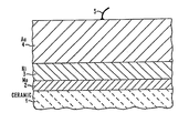
- Ceramic substrate 1 is metallized by a layer 2 of, for example, molybdenum which is personalized or shaped by conventional lithography techniques into a pattern of desired electrical contact areas (not shown), as is well understood in the semiconductor chip packaging art.
- a nickel layer 3 typically is placed over the molybdenum contact area in preparation for a thick or heavy gold deposit 4 which is required for thermocompression bonding of a wire 5, as generally described in the aforementioned February 1978 Technical Disclosure Bulletin.
- an immersion gold layer of about 70 to about 120 nm thickness placed upon the nickel without any further step to enhance the diffusion of the gold into the nickel.
- Selective masking is applied to cover those nickel areas which are not to receive any thermocompression bonding.
- the undiffused immersion gold is removed from the the un masked areas by a chemical stripper immediately before the heavy gold is electroplated upon the unmasked nickel. It is preferred to use a chemical stripper for removing the immersion gold characterized by the following constituents and approximate concentrations:
- the selective masking is removed and the heavy gold is diffused into the nickel with preferably a 550 ° C heat treatment cycle to produce a metallurgical system characterized by reduced hardness and enhanced pull strength relative to that attainable using the prior art processes cited.
- step 5 The undiffused thin gold layer resulting from step 5 is etched away in step 10 of the present invention and rinsed (step 11). Then the remaining steps 11 -14 of the prior process are used as steps 12-15 of the present present invention. Finally, the postponed gold diffusion step is exercised in step 16 and is followed by a plasma ash to form a Au-Ni diffusion barrier necessary to assure proper metallurgy and subsequent bondability in the use of the present invention.
Landscapes
- Engineering & Computer Science (AREA)
- Chemical & Material Sciences (AREA)
- Ceramic Engineering (AREA)
- Manufacturing & Machinery (AREA)
- Microelectronics & Electronic Packaging (AREA)
- Materials Engineering (AREA)
- Structural Engineering (AREA)
- Organic Chemistry (AREA)
- General Physics & Mathematics (AREA)
- Condensed Matter Physics & Semiconductors (AREA)
- Physics & Mathematics (AREA)
- Computer Hardware Design (AREA)
- Power Engineering (AREA)
- Mechanical Engineering (AREA)
- Chemically Coating (AREA)
- Wire Bonding (AREA)
- Manufacturing Of Printed Wiring (AREA)
- Internal Circuitry In Semiconductor Integrated Circuit Devices (AREA)
- ing And Chemical Polishing (AREA)
- Die Bonding (AREA)
- Electroplating Methods And Accessories (AREA)
Claims (8)
Applications Claiming Priority (2)
| Application Number | Priority Date | Filing Date | Title |
|---|---|---|---|
| US735040 | 1985-05-17 | ||
| US06/735,040 US4601424A (en) | 1985-05-17 | 1985-05-17 | Stripped gold plating process |
Publications (2)
| Publication Number | Publication Date |
|---|---|
| EP0203423A1 EP0203423A1 (fr) | 1986-12-03 |
| EP0203423B1 true EP0203423B1 (fr) | 1989-09-27 |
Family
ID=24954106
Family Applications (1)
| Application Number | Title | Priority Date | Filing Date |
|---|---|---|---|
| EP86106186A Expired EP0203423B1 (fr) | 1985-05-17 | 1986-05-06 | Procédé pour la formation d'un système métallurgique comprenant une couche de base en nickel et une couche supérieure en or |
Country Status (5)
| Country | Link |
|---|---|
| US (1) | US4601424A (fr) |
| EP (1) | EP0203423B1 (fr) |
| JP (1) | JPS61265853A (fr) |
| CA (1) | CA1232497A (fr) |
| DE (1) | DE3665858D1 (fr) |
Families Citing this family (12)
| Publication number | Priority date | Publication date | Assignee | Title |
|---|---|---|---|---|
| JPH0813898B2 (ja) * | 1985-08-06 | 1996-02-14 | 呉羽化学工業株式会社 | 燻煙処理可能な食品包装フイルム |
| JP2781017B2 (ja) * | 1989-09-04 | 1998-07-30 | 新光電気工業株式会社 | セラミックパッケージ |
| US5038195A (en) * | 1990-02-09 | 1991-08-06 | Ibm | Composition and coating to prevent current induced electrochemical dendrite formation between conductors on dielectric substrate |
| DE4107142A1 (de) * | 1991-01-24 | 1992-07-30 | Hoechst Ceram Tec Ag | Verfahren zur herstellung von edelmetallbeschichteten schichten eines unedlen metalls |
| US5548486A (en) * | 1994-01-21 | 1996-08-20 | International Business Machines Corporation | Pinned module |
| JP3000877B2 (ja) | 1995-02-20 | 2000-01-17 | 松下電器産業株式会社 | 金メッキ電極の形成方法、基板及びワイヤボンディング方法 |
| US5878483A (en) * | 1995-06-01 | 1999-03-09 | International Business Machines Corporation | Hammer for forming bulges in an array of compliant pin blanks |
| JPH10242205A (ja) * | 1997-03-03 | 1998-09-11 | Hitachi Chem Co Ltd | ワイヤボンディング端子とその形成方法 |
| DE10311031B4 (de) * | 2003-03-13 | 2005-04-21 | Siemens Ag | Elektrochemischer Sensor und Verfahren zu dessen Herstellung |
| JP2005268672A (ja) * | 2004-03-22 | 2005-09-29 | Mitsubishi Electric Corp | 基板 |
| JP5927996B2 (ja) * | 2012-03-02 | 2016-06-01 | 日産自動車株式会社 | モータ配線構造 |
| CN109211992B (zh) * | 2017-06-29 | 2024-07-19 | 深圳市理邦精密仪器股份有限公司 | 用于血气生化测量的电极电路板以及制作电极的方法 |
Family Cites Families (8)
| Publication number | Priority date | Publication date | Assignee | Title |
|---|---|---|---|---|
| GB1031837A (en) * | 1963-08-01 | 1966-06-02 | Standard Telephones Cables Ltd | Improvements in or relating to metal plating |
| US3386906A (en) * | 1965-11-26 | 1968-06-04 | Philips Corp | Transistor base and method of making the same |
| DE1299769B (de) * | 1966-08-26 | 1969-07-24 | Bosch Gmbh Robert | Verfahren zur Kontaktierung einer Halbleiteranordnung |
| US3982908A (en) * | 1975-11-20 | 1976-09-28 | Rca Corporation | Nickel-gold-cobalt contact for silicon devices |
| US4268849A (en) * | 1978-11-03 | 1981-05-19 | National Semiconductor Corporation | Raised bonding pad |
| US4268584A (en) * | 1979-12-17 | 1981-05-19 | International Business Machines Corporation | Nickel-X/gold/nickel-X conductors for solid state devices where X is phosphorus, boron, or carbon |
| JPS5852900A (ja) * | 1981-09-24 | 1983-03-29 | 株式会社日立製作所 | セラミツク多層配線板の製造方法 |
| US4442137A (en) * | 1982-03-18 | 1984-04-10 | International Business Machines Corporation | Maskless coating of metallurgical features of a dielectric substrate |
-
1985
- 1985-05-17 US US06/735,040 patent/US4601424A/en not_active Expired - Fee Related
-
1986
- 1986-01-31 CA CA000500847A patent/CA1232497A/fr not_active Expired
- 1986-03-03 JP JP61044277A patent/JPS61265853A/ja active Granted
- 1986-05-06 EP EP86106186A patent/EP0203423B1/fr not_active Expired
- 1986-05-06 DE DE8686106186T patent/DE3665858D1/de not_active Expired
Also Published As
| Publication number | Publication date |
|---|---|
| DE3665858D1 (en) | 1989-11-02 |
| US4601424A (en) | 1986-07-22 |
| JPH0253945B2 (fr) | 1990-11-20 |
| CA1232497A (fr) | 1988-02-09 |
| EP0203423A1 (fr) | 1986-12-03 |
| JPS61265853A (ja) | 1986-11-25 |
Similar Documents
| Publication | Publication Date | Title |
|---|---|---|
| US4182781A (en) | Low cost method for forming elevated metal bumps on integrated circuit bodies employing an aluminum/palladium metallization base for electroless plating | |
| US5907790A (en) | Aluminum-palladium alloy for initiation of electroless plating | |
| EP0535864B1 (fr) | Fabrication d'une région conductrice dans des dispositifs électroniques | |
| DE19581952B4 (de) | Verfahren zum Entfernen von Metallschichten von einer Pb/Sn-Lötbumps aufweisenden Substratoberfläche | |
| EP0203423B1 (fr) | Procédé pour la formation d'un système métallurgique comprenant une couche de base en nickel et une couche supérieure en or | |
| US3761309A (en) | Ctor components into housings method of producing soft solderable contacts for installing semicondu | |
| EP0176746B1 (fr) | Fabrication de plots de contact en cuivre pour circuits intégrés | |
| US20010020745A1 (en) | An interconnect component for a semiconductor die including a ruthenium layer and a method for its fabrication | |
| TW200931548A (en) | Method for manufacturing a substrate for mounting a semiconductor element | |
| US4767049A (en) | Special surfaces for wire bonding | |
| US20020111022A1 (en) | Method of forming embedded copper interconnections and embedded copper interconnection structure | |
| US3890177A (en) | Technique for the fabrication of air-isolated crossovers | |
| JPS61152042A (ja) | 半導体素子の金属化パターンおよびその方法 | |
| US4065588A (en) | Method of making gold-cobalt contact for silicon devices | |
| JP2002289653A (ja) | 半導体装置用テープキャリアおよびその製造方法 | |
| WO1998034278A1 (fr) | Materiau pour cadre de montage | |
| JPH10233121A (ja) | リードワイヤ | |
| JPH02253628A (ja) | 半導体装置の製造方法 | |
| JP2002289652A (ja) | 半導体装置用テープキャリアおよびその製造方法 | |
| JPS63122248A (ja) | 半導体装置の製造方法 | |
| US5308686A (en) | Substrate having a multiple metal protected conductive layer and method of manufacturing the same | |
| JPH0256436B2 (fr) | ||
| JP2000307219A (ja) | 配線基板およびその製造方法 | |
| US3716428A (en) | Method of etching a metal which can be passivated | |
| KR100215996B1 (ko) | 철-니켈 합금 소재의 내식성 및 내균열성 향상을 위한 4층 도금 방법 |
Legal Events
| Date | Code | Title | Description |
|---|---|---|---|
| PUAI | Public reference made under article 153(3) epc to a published international application that has entered the european phase |
Free format text: ORIGINAL CODE: 0009012 |
|
| AK | Designated contracting states |
Kind code of ref document: A1 Designated state(s): DE FR GB IT |
|
| 17P | Request for examination filed |
Effective date: 19870327 |
|
| 17Q | First examination report despatched |
Effective date: 19880316 |
|
| GRAA | (expected) grant |
Free format text: ORIGINAL CODE: 0009210 |
|
| AK | Designated contracting states |
Kind code of ref document: B1 Designated state(s): DE FR GB IT |
|
| PG25 | Lapsed in a contracting state [announced via postgrant information from national office to epo] |
Ref country code: IT Free format text: LAPSE BECAUSE OF FAILURE TO SUBMIT A TRANSLATION OF THE DESCRIPTION OR TO PAY THE FEE WITHIN THE PRESCRIBED TIME-LIMIT;WARNING: LAPSES OF ITALIAN PATENTS WITH EFFECTIVE DATE BEFORE 2007 MAY HAVE OCCURRED AT ANY TIME BEFORE 2007. THE CORRECT EFFECTIVE DATE MAY BE DIFFERENT FROM THE ONE RECORDED. Effective date: 19890927 |
|
| REF | Corresponds to: |
Ref document number: 3665858 Country of ref document: DE Date of ref document: 19891102 |
|
| ET | Fr: translation filed | ||
| PLBE | No opposition filed within time limit |
Free format text: ORIGINAL CODE: 0009261 |
|
| STAA | Information on the status of an ep patent application or granted ep patent |
Free format text: STATUS: NO OPPOSITION FILED WITHIN TIME LIMIT |
|
| 26N | No opposition filed | ||
| PGFP | Annual fee paid to national office [announced via postgrant information from national office to epo] |
Ref country code: GB Payment date: 19960422 Year of fee payment: 11 |
|
| PGFP | Annual fee paid to national office [announced via postgrant information from national office to epo] |
Ref country code: FR Payment date: 19960507 Year of fee payment: 11 |
|
| PGFP | Annual fee paid to national office [announced via postgrant information from national office to epo] |
Ref country code: DE Payment date: 19960529 Year of fee payment: 11 |
|
| PG25 | Lapsed in a contracting state [announced via postgrant information from national office to epo] |
Ref country code: GB Effective date: 19970506 |
|
| GBPC | Gb: european patent ceased through non-payment of renewal fee |
Effective date: 19970506 |
|
| PG25 | Lapsed in a contracting state [announced via postgrant information from national office to epo] |
Ref country code: FR Free format text: LAPSE BECAUSE OF NON-PAYMENT OF DUE FEES Effective date: 19980130 |
|
| PG25 | Lapsed in a contracting state [announced via postgrant information from national office to epo] |
Ref country code: DE Free format text: LAPSE BECAUSE OF NON-PAYMENT OF DUE FEES Effective date: 19980203 |
|
| REG | Reference to a national code |
Ref country code: FR Ref legal event code: ST |