EP0202705B1 - Polyimidbildschicht, lichtempfindliche Polyimidsäurederivat und elektrophoretische Anzeigezelle - Google Patents
Polyimidbildschicht, lichtempfindliche Polyimidsäurederivat und elektrophoretische Anzeigezelle Download PDFInfo
- Publication number
- EP0202705B1 EP0202705B1 EP86200758A EP86200758A EP0202705B1 EP 0202705 B1 EP0202705 B1 EP 0202705B1 EP 86200758 A EP86200758 A EP 86200758A EP 86200758 A EP86200758 A EP 86200758A EP 0202705 B1 EP0202705 B1 EP 0202705B1
- Authority
- EP
- European Patent Office
- Prior art keywords
- polyamide acid
- acid derivative
- formula
- compound
- layer
- Prior art date
- Legal status (The legal status is an assumption and is not a legal conclusion. Google has not performed a legal analysis and makes no representation as to the accuracy of the status listed.)
- Expired - Lifetime
Links
- 239000004952 Polyamide Substances 0.000 title claims description 69
- 229920002647 polyamide Polymers 0.000 title claims description 69
- 239000002253 acid Substances 0.000 title claims description 68
- 229920001721 polyimide Polymers 0.000 title claims description 21
- 150000001875 compounds Chemical class 0.000 claims description 34
- 238000000034 method Methods 0.000 claims description 31
- 229920002120 photoresistant polymer Polymers 0.000 claims description 24
- 239000000758 substrate Substances 0.000 claims description 19
- 239000004642 Polyimide Substances 0.000 claims description 18
- 210000004027 cell Anatomy 0.000 claims description 17
- 125000004435 hydrogen atom Chemical group [H]* 0.000 claims description 16
- 239000000203 mixture Substances 0.000 claims description 14
- 238000010521 absorption reaction Methods 0.000 claims description 12
- 125000004432 carbon atom Chemical group C* 0.000 claims description 12
- 125000000217 alkyl group Chemical group 0.000 claims description 8
- 210000002421 cell wall Anatomy 0.000 claims description 8
- 125000002496 methyl group Chemical group [H]C([H])([H])* 0.000 claims description 8
- 238000010438 heat treatment Methods 0.000 claims description 5
- 125000002947 alkylene group Chemical group 0.000 claims description 4
- 125000001495 ethyl group Chemical group [H]C([H])([H])C([H])([H])* 0.000 claims description 4
- 125000004430 oxygen atom Chemical group O* 0.000 claims description 4
- 229920003229 poly(methyl methacrylate) Polymers 0.000 claims description 4
- 239000004926 polymethyl methacrylate Substances 0.000 claims description 4
- 238000002211 ultraviolet spectrum Methods 0.000 claims description 4
- 239000010410 layer Substances 0.000 description 47
- GWEVSGVZZGPLCZ-UHFFFAOYSA-N Titan oxide Chemical compound O=[Ti]=O GWEVSGVZZGPLCZ-UHFFFAOYSA-N 0.000 description 8
- 125000003178 carboxy group Chemical group [H]OC(*)=O 0.000 description 8
- 239000002245 particle Substances 0.000 description 8
- 239000011651 chromium Substances 0.000 description 7
- FQPSGWSUVKBHSU-UHFFFAOYSA-N methacrylamide Chemical group CC(=C)C(N)=O FQPSGWSUVKBHSU-UHFFFAOYSA-N 0.000 description 7
- MVPPADPHJFYWMZ-UHFFFAOYSA-N chlorobenzene Chemical compound ClC1=CC=CC=C1 MVPPADPHJFYWMZ-UHFFFAOYSA-N 0.000 description 6
- VYZAMTAEIAYCRO-UHFFFAOYSA-N Chromium Chemical compound [Cr] VYZAMTAEIAYCRO-UHFFFAOYSA-N 0.000 description 5
- 238000006243 chemical reaction Methods 0.000 description 5
- 229910052804 chromium Inorganic materials 0.000 description 5
- 238000004519 manufacturing process Methods 0.000 description 5
- 229910003437 indium oxide Inorganic materials 0.000 description 4
- PJXISJQVUVHSOJ-UHFFFAOYSA-N indium(iii) oxide Chemical compound [O-2].[O-2].[O-2].[In+3].[In+3] PJXISJQVUVHSOJ-UHFFFAOYSA-N 0.000 description 4
- OKKJLVBELUTLKV-UHFFFAOYSA-N Methanol Chemical compound OC OKKJLVBELUTLKV-UHFFFAOYSA-N 0.000 description 3
- SECXISVLQFMRJM-UHFFFAOYSA-N N-Methylpyrrolidone Chemical compound CN1CCCC1=O SECXISVLQFMRJM-UHFFFAOYSA-N 0.000 description 3
- 239000011521 glass Substances 0.000 description 3
- -1 methacrylate compound Chemical class 0.000 description 3
- 239000002904 solvent Substances 0.000 description 3
- 229920003002 synthetic resin Polymers 0.000 description 3
- 239000000057 synthetic resin Substances 0.000 description 3
- XOLBLPGZBRYERU-UHFFFAOYSA-N tin dioxide Chemical compound O=[Sn]=O XOLBLPGZBRYERU-UHFFFAOYSA-N 0.000 description 3
- 229910001887 tin oxide Inorganic materials 0.000 description 3
- JNDVNJWCRZQGFQ-UHFFFAOYSA-N 2-methyl-N,N-bis(methylamino)hex-2-enamide Chemical compound CCCC=C(C)C(=O)N(NC)NC JNDVNJWCRZQGFQ-UHFFFAOYSA-N 0.000 description 2
- VVBLNCFGVYUYGU-UHFFFAOYSA-N 4,4'-Bis(dimethylamino)benzophenone Chemical compound C1=CC(N(C)C)=CC=C1C(=O)C1=CC=C(N(C)C)C=C1 VVBLNCFGVYUYGU-UHFFFAOYSA-N 0.000 description 2
- NTIZESTWPVYFNL-UHFFFAOYSA-N Methyl isobutyl ketone Chemical compound CC(C)CC(C)=O NTIZESTWPVYFNL-UHFFFAOYSA-N 0.000 description 2
- UIHCLUNTQKBZGK-UHFFFAOYSA-N Methyl isobutyl ketone Natural products CCC(C)C(C)=O UIHCLUNTQKBZGK-UHFFFAOYSA-N 0.000 description 2
- 125000003277 amino group Chemical group 0.000 description 2
- 230000000536 complexating effect Effects 0.000 description 2
- 230000003247 decreasing effect Effects 0.000 description 2
- 239000000975 dye Substances 0.000 description 2
- 230000002349 favourable effect Effects 0.000 description 2
- 239000007788 liquid Substances 0.000 description 2
- 229910052751 metal Inorganic materials 0.000 description 2
- 239000002184 metal Substances 0.000 description 2
- 229940043265 methyl isobutyl ketone Drugs 0.000 description 2
- WFKDPJRCBCBQNT-UHFFFAOYSA-N n,2-dimethylprop-2-enamide Chemical compound CNC(=O)C(C)=C WFKDPJRCBCBQNT-UHFFFAOYSA-N 0.000 description 2
- SJIXRGNQPBQWMK-UHFFFAOYSA-N 2-(diethylamino)ethyl 2-methylprop-2-enoate Chemical compound CCN(CC)CCOC(=O)C(C)=C SJIXRGNQPBQWMK-UHFFFAOYSA-N 0.000 description 1
- JKNCOURZONDCGV-UHFFFAOYSA-N 2-(dimethylamino)ethyl 2-methylprop-2-enoate Chemical compound CN(C)CCOC(=O)C(C)=C JKNCOURZONDCGV-UHFFFAOYSA-N 0.000 description 1
- KZUIKPMQAIEBOE-UHFFFAOYSA-N 2-(ethylamino)ethyl 2-methylprop-2-enoate Chemical compound CCNCCOC(=O)C(C)=C KZUIKPMQAIEBOE-UHFFFAOYSA-N 0.000 description 1
- DEGZUQBZHACZKW-UHFFFAOYSA-N 2-(methylamino)ethyl 2-methylprop-2-enoate Chemical compound CNCCOC(=O)C(C)=C DEGZUQBZHACZKW-UHFFFAOYSA-N 0.000 description 1
- WWJCRUKUIQRCGP-UHFFFAOYSA-N 3-(dimethylamino)propyl 2-methylprop-2-enoate Chemical compound CN(C)CCCOC(=O)C(C)=C WWJCRUKUIQRCGP-UHFFFAOYSA-N 0.000 description 1
- 241000167854 Bourreria succulenta Species 0.000 description 1
- FXHOOIRPVKKKFG-UHFFFAOYSA-N N,N-Dimethylacetamide Chemical compound CN(C)C(C)=O FXHOOIRPVKKKFG-UHFFFAOYSA-N 0.000 description 1
- DFPAKSUCGFBDDF-UHFFFAOYSA-N Nicotinamide Chemical group NC(=O)C1=CC=CN=C1 DFPAKSUCGFBDDF-UHFFFAOYSA-N 0.000 description 1
- 239000007795 chemical reaction product Substances 0.000 description 1
- 235000019693 cherries Nutrition 0.000 description 1
- 238000010276 construction Methods 0.000 description 1
- 125000002147 dimethylamino group Chemical group [H]C([H])([H])N(*)C([H])([H])[H] 0.000 description 1
- 230000008020 evaporation Effects 0.000 description 1
- 238000001704 evaporation Methods 0.000 description 1
- 229910052739 hydrogen Inorganic materials 0.000 description 1
- 239000001257 hydrogen Substances 0.000 description 1
- 238000005468 ion implantation Methods 0.000 description 1
- 150000002576 ketones Chemical class 0.000 description 1
- 239000000463 material Substances 0.000 description 1
- 239000011159 matrix material Substances 0.000 description 1
- 229910044991 metal oxide Inorganic materials 0.000 description 1
- 150000004706 metal oxides Chemical class 0.000 description 1
- ZIWDVJPPVMGJGR-UHFFFAOYSA-N n-ethyl-2-methylprop-2-enamide Chemical compound CCNC(=O)C(C)=C ZIWDVJPPVMGJGR-UHFFFAOYSA-N 0.000 description 1
- 239000012299 nitrogen atmosphere Substances 0.000 description 1
- 229920000642 polymer Polymers 0.000 description 1
- 239000002243 precursor Substances 0.000 description 1
- 239000000047 product Substances 0.000 description 1
- 239000011241 protective layer Substances 0.000 description 1
- 239000010453 quartz Substances 0.000 description 1
- 239000001044 red dye Substances 0.000 description 1
- 239000004065 semiconductor Substances 0.000 description 1
- VYPSYNLAJGMNEJ-UHFFFAOYSA-N silicon dioxide Inorganic materials O=[Si]=O VYPSYNLAJGMNEJ-UHFFFAOYSA-N 0.000 description 1
- 125000006850 spacer group Chemical group 0.000 description 1
- 238000001228 spectrum Methods 0.000 description 1
- 238000004544 sputter deposition Methods 0.000 description 1
- 238000003756 stirring Methods 0.000 description 1
- 239000000126 substance Substances 0.000 description 1
- 238000001771 vacuum deposition Methods 0.000 description 1
Images


Classifications
-
- G—PHYSICS
- G03—PHOTOGRAPHY; CINEMATOGRAPHY; ANALOGOUS TECHNIQUES USING WAVES OTHER THAN OPTICAL WAVES; ELECTROGRAPHY; HOLOGRAPHY
- G03F—PHOTOMECHANICAL PRODUCTION OF TEXTURED OR PATTERNED SURFACES, e.g. FOR PRINTING, FOR PROCESSING OF SEMICONDUCTOR DEVICES; MATERIALS THEREFOR; ORIGINALS THEREFOR; APPARATUS SPECIALLY ADAPTED THEREFOR
- G03F7/00—Photomechanical, e.g. photolithographic, production of textured or patterned surfaces, e.g. printing surfaces; Materials therefor, e.g. comprising photoresists; Apparatus specially adapted therefor
- G03F7/004—Photosensitive materials
- G03F7/038—Macromolecular compounds which are rendered insoluble or differentially wettable
- G03F7/0387—Polyamides or polyimides
-
- C—CHEMISTRY; METALLURGY
- C08—ORGANIC MACROMOLECULAR COMPOUNDS; THEIR PREPARATION OR CHEMICAL WORKING-UP; COMPOSITIONS BASED THEREON
- C08G—MACROMOLECULAR COMPOUNDS OBTAINED OTHERWISE THAN BY REACTIONS ONLY INVOLVING UNSATURATED CARBON-TO-CARBON BONDS
- C08G73/00—Macromolecular compounds obtained by reactions forming a linkage containing nitrogen with or without oxygen or carbon in the main chain of the macromolecule, not provided for in groups C08G12/00 - C08G71/00
- C08G73/06—Polycondensates having nitrogen-containing heterocyclic rings in the main chain of the macromolecule
- C08G73/10—Polyimides; Polyester-imides; Polyamide-imides; Polyamide acids or similar polyimide precursors
- C08G73/1003—Preparatory processes
- C08G73/1007—Preparatory processes from tetracarboxylic acids or derivatives and diamines
- C08G73/1025—Preparatory processes from tetracarboxylic acids or derivatives and diamines polymerised by radiations
-
- G—PHYSICS
- G02—OPTICS
- G02F—OPTICAL DEVICES OR ARRANGEMENTS FOR THE CONTROL OF LIGHT BY MODIFICATION OF THE OPTICAL PROPERTIES OF THE MEDIA OF THE ELEMENTS INVOLVED THEREIN; NON-LINEAR OPTICS; FREQUENCY-CHANGING OF LIGHT; OPTICAL LOGIC ELEMENTS; OPTICAL ANALOGUE/DIGITAL CONVERTERS
- G02F1/00—Devices or arrangements for the control of the intensity, colour, phase, polarisation or direction of light arriving from an independent light source, e.g. switching, gating or modulating; Non-linear optics
- G02F1/01—Devices or arrangements for the control of the intensity, colour, phase, polarisation or direction of light arriving from an independent light source, e.g. switching, gating or modulating; Non-linear optics for the control of the intensity, phase, polarisation or colour
- G02F1/0102—Constructional details, not otherwise provided for in this subclass
-
- G—PHYSICS
- G02—OPTICS
- G02F—OPTICAL DEVICES OR ARRANGEMENTS FOR THE CONTROL OF LIGHT BY MODIFICATION OF THE OPTICAL PROPERTIES OF THE MEDIA OF THE ELEMENTS INVOLVED THEREIN; NON-LINEAR OPTICS; FREQUENCY-CHANGING OF LIGHT; OPTICAL LOGIC ELEMENTS; OPTICAL ANALOGUE/DIGITAL CONVERTERS
- G02F1/00—Devices or arrangements for the control of the intensity, colour, phase, polarisation or direction of light arriving from an independent light source, e.g. switching, gating or modulating; Non-linear optics
- G02F1/01—Devices or arrangements for the control of the intensity, colour, phase, polarisation or direction of light arriving from an independent light source, e.g. switching, gating or modulating; Non-linear optics for the control of the intensity, phase, polarisation or colour
- G02F1/165—Devices or arrangements for the control of the intensity, colour, phase, polarisation or direction of light arriving from an independent light source, e.g. switching, gating or modulating; Non-linear optics for the control of the intensity, phase, polarisation or colour based on translational movement of particles in a fluid under the influence of an applied field
- G02F1/166—Devices or arrangements for the control of the intensity, colour, phase, polarisation or direction of light arriving from an independent light source, e.g. switching, gating or modulating; Non-linear optics for the control of the intensity, phase, polarisation or colour based on translational movement of particles in a fluid under the influence of an applied field characterised by the electro-optical or magneto-optical effect
- G02F1/167—Devices or arrangements for the control of the intensity, colour, phase, polarisation or direction of light arriving from an independent light source, e.g. switching, gating or modulating; Non-linear optics for the control of the intensity, phase, polarisation or colour based on translational movement of particles in a fluid under the influence of an applied field characterised by the electro-optical or magneto-optical effect by electrophoresis
-
- G—PHYSICS
- G03—PHOTOGRAPHY; CINEMATOGRAPHY; ANALOGOUS TECHNIQUES USING WAVES OTHER THAN OPTICAL WAVES; ELECTROGRAPHY; HOLOGRAPHY
- G03F—PHOTOMECHANICAL PRODUCTION OF TEXTURED OR PATTERNED SURFACES, e.g. FOR PRINTING, FOR PROCESSING OF SEMICONDUCTOR DEVICES; MATERIALS THEREFOR; ORIGINALS THEREFOR; APPARATUS SPECIALLY ADAPTED THEREFOR
- G03F7/00—Photomechanical, e.g. photolithographic, production of textured or patterned surfaces, e.g. printing surfaces; Materials therefor, e.g. comprising photoresists; Apparatus specially adapted therefor
- G03F7/004—Photosensitive materials
- G03F7/09—Photosensitive materials characterised by structural details, e.g. supports, auxiliary layers
- G03F7/095—Photosensitive materials characterised by structural details, e.g. supports, auxiliary layers having more than one photosensitive layer
-
- G—PHYSICS
- G02—OPTICS
- G02F—OPTICAL DEVICES OR ARRANGEMENTS FOR THE CONTROL OF LIGHT BY MODIFICATION OF THE OPTICAL PROPERTIES OF THE MEDIA OF THE ELEMENTS INVOLVED THEREIN; NON-LINEAR OPTICS; FREQUENCY-CHANGING OF LIGHT; OPTICAL LOGIC ELEMENTS; OPTICAL ANALOGUE/DIGITAL CONVERTERS
- G02F1/00—Devices or arrangements for the control of the intensity, colour, phase, polarisation or direction of light arriving from an independent light source, e.g. switching, gating or modulating; Non-linear optics
- G02F1/01—Devices or arrangements for the control of the intensity, colour, phase, polarisation or direction of light arriving from an independent light source, e.g. switching, gating or modulating; Non-linear optics for the control of the intensity, phase, polarisation or colour
- G02F1/165—Devices or arrangements for the control of the intensity, colour, phase, polarisation or direction of light arriving from an independent light source, e.g. switching, gating or modulating; Non-linear optics for the control of the intensity, phase, polarisation or colour based on translational movement of particles in a fluid under the influence of an applied field
- G02F1/1675—Constructional details
- G02F1/16756—Insulating layers
Definitions
- the invention relates to a method of forming on a substrate a patterned polyimide film which is provided with an electrically conductive layer at the upper surface facing away from the substrate.
- German Patent Specification 2 914 619 describes a method of forming a polyimide pattern on a substrate.
- the substrate is provided with a layer of a photosensitive polyamide acid derivative which is then exposed patternwise to UV light, developed and finally converted to polyimide by subjecting it to a heat treatment.
- a method as described above which is characterized in that the substrate is provided with a layer of a photosensitive polyamide acid derivative onto which a layer of a positive photoresist is applied, after which the assembly is exposed patternwise, the photoresist layer is developed, an electrcially conductive layer is applied to the photoresist layer which then removed by means of a lift-off process, the non-exposed parts of the layer of polyamide acid derivative are removed and the remaining exposed parts are subjected to a heat treatment and imidised to form polyimide.
- the invention has the important and surprising advantage that the polyimide pattern obtained has very straight wall portions which are perpendicular to the substrate.
- An advantageous embodiment of the method in accordance with the invention is characterized in that a positive photoresist is used whose absorption wavelength differs from that of the photosensitive polyamide acid derivative, the exposure of the assembly in accordance with a certain pattern being carried out in two successive steps, the first step consisting in exposing the assembly in accordance with a certain pattern to light whose emission wavelength corresponds to the absorption wavelength of the photoresist, and the second step consisting in exposing the assembly in accordance with a certain pattern to light whose emission wavelength corresponds to the absorption wavelength of the photosensitive polyamide acid derivative.
- This advantageous embodiment has the interesting and practical advantage that the first exposure step, in which the positive photoresist is exposed, is immediately followed by the second. In the second exposure step the polyamide acid derivative is exposed through the positive photoresist. Between the first and the second exposure step no development of the photoresist takes place. This means that, for example, between the first and the second exposure step the mask used for the patterned exposure does not have to be removed and repositioned. In particular the latter measure is costly and time-consuming.
- a positive photoresist having an absorption wavelength in the near UV spectrum and a polyamide acid derivative having an absorption wavelength in the UV spectrum.
- a first exposure step the assembly is exposed to a deep UV light and, subsequently, in the second step to UV light.
- the positive photoresist which is not developed after the first exposure step transmits the UV light used in the second exposure step, such that the photosensitive polyamide acid derivative is actually exposed.
- the wavelength range of DUV light is approximately 180-260 nm, that of UV light is approximately 260 to 450 nm.
- a suitable positive photoresist is p-isopropenyl methylketone.
- positive photoresist whose absorption wavelength is situated in the UV range.
- An example thereof is a Novolak-diazochinone photoresist as marketed by Shipley and Hunt Waycoat. In order to obtain the best results such a photoresist must be developed after the first exposure.
- a photosensitive polyamide acid derivative which is obtained by making polyamide acid react with one or more compounds of formula 1 in which:
- the reaction is carried out at a normal or slightly raised temperature. Use is made of a solvent such as N-methypyrrolidone.
- the end product corresponds to the formula 10.
- the zigzag line represents the polyamide acid chain which contains various carboxyl groups. Two of these carboxyl groups are shown in Figure 10. This carboxyl group forms a salt bridge together with the amino group of the methacrylate compound used, which salt bridge is indicated by a dot.
- the method in accordance with the invention makes use of a polyamide acid derivative which is obtained by making polyamide acid react with one or more compounds and in accordance with formula 2 in which
- the ratio between the number of equivalents of the compounds of formulae 1 and 2 and the number of -COOH equivalents of the polyamide acid is greater than 0.05 and preferably greater than 0.3.
- a suitable mixture contains 10-90 mol.% of a compound of formula 3 and 10-90 mol.% of a compound of formula 4
- the resultant of the reaction between this mixture and polyamide acid is schematically represented in formula 5 in which the zigzag line represents the polyamide acid chain of which two carboxyl groups are shown.
- the remarkable thing about this is that the dimethylamino group of the dimethylaminopropylmethacryl acid amide (formula 3) is connected to a carboxyl group of the polyamide acid by means of a salt bridge, and that the amino group of the methacryl acid amide is connected to a carboxyl group of the polyamide acid or possibly to the acid amide group in the main chain of the polyamide acid by means of H bridges.
- a hydrogen bridge is indicated by three dots.
- Polyamide acid is also called polyimide precursor. It is a known and commercially available product. Reference can be made to U.S. Patent Specification 3,943,065 and to the published Netherlands Patent Application 8,202,688 (PHN 10.389), page 2 lines 6 to 34, filed by Applicants.
- the photoresist layer is developed. In this process the exposed parts dissolve.
- a suitable developer is, for example, a ketone such as methylisobutylketone.
- An electrically conductive layer is applied to the upper surface of the developed photoresist layer.
- This layer is, preferably, of a metal, such as chromium.
- the thickness of the chromium layer is, for example, 100 nm.
- the layer is applied by known methods such as, for example, sputtering or vacuum deposition.
- the next step in the process in accordance with the invention is the removal of the unexposed parts of the polyamide acid derivative.
- this developing step is carried out using dimethylacetamide-mathanol (5:1).
- the exposed parts of the polyamide acid derivative are not removed because, due to exposure, complexing has taken place of the polyamide acid molecules with the polymer molecules developed by photopolymerisation of the compounds of formulae 1 and 2.
- this is shown in formula 6
- two methacrylamide groups are interconnected. This may be methacrylamide groups which are attached to the same polyamide acid chain, as shown in formula 6.
- the interconnected groups may also belong to different polyamide acid chains.
- the exposed polyamide acid derivative is imidised by subjecting it to a heat treatment for, for example, 1 hour at 150 o C and 1 hour at 350 o C.
- the imidisation process is carried out in an N2 atmosphere.
- the invention also relates to a new photosensitive polyamide acid derivative which is obtained by making polyamide acid react with one or more compounds in accordance with formula 7 in which:
- the photosensitive polyamide acid derivative in accordance with the invention may very suitably be used in the above-described method of manufacturing a polyimide structure.
- the polyamide acid derivative may also be used in the common method of manufacturing a polyimide pattern. In the common method, a layer of the polyamide acid derivative is exposed in accordance with a certain pattern, developed and converted to polyimide.
- a very suitable polyamide acid derivative in accordance with the invention is obtained by making polyamide acid react with one or more compounds in accordance with formula 9 in which:
- a very interesting polyamide acid derivative is formed by the resultant of a reaction between polyamide acid and a mixture containing 10-90 mol.% of a compound of formula 3 and 10-90 mol.% of a compound of formula 4.
- a mixture which contains 25 mol.% of the compound in accordance with formula 3 and 75 mol.% of a compound in accordance with formula 4.
- the polyamide acid derivatives formed on the basis of the above-described mixtures have the advantage that shrinkage upon imidisation is reduced from, for example, 40 to 50% in the case of mono-component derivatives of polyamide acid to 30%.
- the above-described method of applying polyimide layers in accordance with a certain pattern as well as the above-stated photosensitive polyamide acid derivates may be used in the manufacture of passivating layers, insulating layers or protective layers and the like of semiconductor arrangements. Alternatively they can be used in the manufacture of miniature circuits or masks for, for example, ion implantation.
- a very interesting field of application is the production of an electrophoretic image-display cell.
- the invention also relates to a new, improved electrophoretic image-display cell comprising two parallel cell walls at least one of which is transparent, one or more electrodes which are provided on the inside surface of each cell wall as well as a net-shaped electrode which is arranged between both cell walls, which net-shaped electrode runs parallel to the said cell walls and is supported by a dielectric layer having a network structure.
- the improvement in accordance with the invention is characterized in that the dielectric layer is made of polyimide.
- the polyimide dielectric layer which is provided with an electrode is arranged in accordance with a certain pattern by implementing the above-described method.
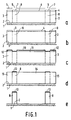
- Reference numeral 1 in Figure 1 denotes a transparent substrate which is made of glass.
- the substrate 1 may also be made of a transparent synthetic resin.
- An electrically conductive layer 2 of, for example, indiumoxide or tinoxide is provided on the substrate 1.
- Layer 3 has a thickness of, for example, 13 ⁇ m.
- Layer 3 is provided by dissolving the photosensitive polyamide acid derivative in a suitable solvent, such as N-methylpyrrolidone (15-20% solution). The solution is applied to layer 2 and the solvent is evaporated.
- the said solution of the photosensitive polyamide acid derivative is obtained by dissolving polyamide acid and a mixture of 25 mol.% of N,N-dimethylaminopropylmethacrylamide (formula 3) and 75 mol.% of methacrylamide (formula 4) in N-methylpyrrolidone and stirring the solution at room temperature for 30 minutes.
- the number of equivalents of N,N-dimethylaminopropylmethacrylamide corresponds to one fourth of the number of -COOH equivalents of the polyamide acid.
- a photoinitiator, such as Michler's ketone, is also added to the solution.
- a layer 4 of polymethylmethacrylate having a thickness of 0.1-0.2 ⁇ m is applied to layer 3.
- a solution of PMMA in chlorobenzene is used.
- the layers 3 and 4 are exposed through openings 6 in a quartz mask 5.
- the exposure is carried out in two steps.
- the first exposure step is carried out using D U V. having a wavelength of 220 nm.
- the portions 7 of layer 4 are exposed.
- U V - light having a wavelength of 360 nm is used to expose the portions 8 of layer 3.
- the exposed portions 7 of layer 4 are removed by treating (developing) them with methylisobutylketone ( Figure 1b).
- a layer of chromium 10 having a thickness of 100 nm is applied by evaporation ( Figure 1c).
- the unexposed portions 11 and 12 of layer 4 as well as the chromium layer 10 present on these portions are removed by subjecting them to a chlorobenzene treatment (lift-off proces) ( Figure 1d).
- the unexposed portions 14 and 15 of layer 3 are removed (developed) using a mixture 5:1 of dimethylacetamide and methanol ( Figure 1e).
- the remaining portions 8 of layer 3 which are provided on the upper surface with a chromium layer 13 are imidised by heating them at 150°C for 1 hour and at 350°C for 1 hour.
- An electrophoretic image-display cell is shown in perspective in Figure 2.
- An electrophoretic image-display cell is known from for example, Proceedings Conf. '80, Biennical Display Research Conf., Cherry Hill, USA, October 21-28, 1980.
- Reference numeral 20 in Figure 2 denotes a transparent substrate plate which is made of, for example, glass or a transparent synthetic resin.
- So-called row electrodes 21 are provided on the substrate 20, which electrodes are made of, for example, transparent indium oxide or tin oxide.
- the electrodes 21 have a thickness of a few microns.
- the width of each row electrode is approximately 220 ⁇ m, the interspace between the row electrodes is 30 ⁇ m.
- Column electrodes 22 are provided at a distance of approximately 11 ⁇ m from the row electrodes.
- Each column electrode has a width of approximately 220 ⁇ m.
- the interspace between the individual column electrodes is 30 ⁇ m.
- Each column electrode has a network structure 23 as is clearly shown in Figure 3.
- the column electrode is made of, for example, Cr and has a thickness of approximately 0.1. ⁇ m.
- the column or net-shaped electrode 22 is supported by a dielectric layer 24 which has the same network structure as the column electrode 22.
- the dielectric layer 24 is supported by the row electrode 21.
- the dielectric network layer 24 consists of polyimide.
- This polyimide pattern and the column electrode 22 situated thereon can be produced by the above described method ( Figure 1). Surprisingly it has been found that by carrying out the method in accordance with the invention very straight wall portions of the polyimide pattern are obtained. Thanks to these straight wall portions, the quality and particularly the functioning of the image display cell are very much improved.
- An anode 25 is provided at a distance of 50 ⁇ m from the column electrodes 22.
- Anode 25 is made of, for example, indium oxide or tin oxide.
- Anode 25 is supported by a supporting plate 26 which may be made of a transparent or untransparent material such as glass, synthetic resin.
- Substrate 20 and supporting plate 26 are interconnected at the location of the outer edge by means of an annular spacer which is not shown in the Figures.
- the dimensions of the image-display cell are not clearly defined. Consequently, they may vary substantially.
- a suitable size is, for example, 4 x 6 cm or 9 x 16 cm. In the latter case the image-display cell contains 360 row electrodes and 640 column electrodes.
- the operation of the image-display cell is again explained by means of Figure 4.
- Components of Figure 4 which correspond to components of the Figures 2 and 3, bear the same reference numerals.
- the image-display cell is filled with a cell medium 27 which contains a dielectric liquid in which charged particles 28 are dispersed.
- the particles are, for example, negatively charged TiO2 particles.
- a dye is dissolved in the dielectic liquid, for example, a red dye which contrasts with the white colour of the TiO2 particels.
- the anode 25 has a positive voltage of 100 V. All TiO2 particles 28 are situated against the anode 25. Consequently, the image-display cell, which is looked at through substrate 20, has the colour of the dye dissolved in the medium, which is red in this case.
- the column electrodes have a voltage of, for example, 0 V and the row electrodes have a voltage of 30 V. By decreasing the anode voltage to 0 V, the particles will move towards the position indicated in Figure 4. The particles are located in the so-called potential wells. If the original voltage of 100 V is again applied to the anode, the particles will remain in the potential wells due to the difference in potential (30 V) between row electrodes 21 and column electrodes 22.
- the image display cell has a white (TiO2) colour. Decreasing the voltage applied to the row electrodes to 15 V and increasing that applied to the column electrodes to 15 V will make the particles move towards the anode. As the row electrodes and the column electrodes are arranged so that they cross each other, a matrix structure is achieved each segment of which is electrically controlled to obtain the desired image.
Landscapes
- Physics & Mathematics (AREA)
- Nonlinear Science (AREA)
- General Physics & Mathematics (AREA)
- Chemical & Material Sciences (AREA)
- Chemical Kinetics & Catalysis (AREA)
- Optics & Photonics (AREA)
- Health & Medical Sciences (AREA)
- Organic Chemistry (AREA)
- Life Sciences & Earth Sciences (AREA)
- Architecture (AREA)
- Engineering & Computer Science (AREA)
- Spectroscopy & Molecular Physics (AREA)
- Polymers & Plastics (AREA)
- Medicinal Chemistry (AREA)
- Structural Engineering (AREA)
- Electrochemistry (AREA)
- Molecular Biology (AREA)
- Exposure And Positioning Against Photoresist Photosensitive Materials (AREA)
- Polymers With Sulfur, Phosphorus Or Metals In The Main Chain (AREA)
- Macromolecular Compounds Obtained By Forming Nitrogen-Containing Linkages In General (AREA)
- Photosensitive Polymer And Photoresist Processing (AREA)
- Electrochromic Elements, Electrophoresis, Or Variable Reflection Or Absorption Elements (AREA)
- Polyamides (AREA)
Claims (12)
- Verfahren zum Bilden eines gemusterten Polyimidfilms auf einem Träger, wobei dieser Film an der vom Träger abgewandten Oberfläche mit einer elektrisch leitenden Schicht versehen ist, dadurch gekennzeichnet, daß der Träger mit einer Schicht eines lichtempfindlichen Polyamidsäurederivats versehen wird, auf der eine Schicht eines positiven Photoresists angebracht wird, wonach das Gebilde mustermäßig belichtet wird, die Photoresistschicht entwickelt wird, eine elektrisch leitende Schicht auf der Photoresistschicht angebracht wird, die danach in einem "Lift-Off"-Verfahren entfernt wird, wonach die nicht belichteten Teile der Polyamidsäurederivatschicht entfernt, die restlichen belichteten Teile einer Wärmebehandlung ausgesetzt und zum Bilden von Polyimid imidisiert werden.
- Verfahren nach Anspruch 1, dadurch gekennzeichnet, daß ein positiver Photoresist verwendet wird, dessen Absorptionswellenlänge von der des photoempfindlichen Polyamidsäurederivats abweicht, wobei die mustermäßige Belichtung des Gebildes in zwei aufeinanderfolgenden Verfahrensschritten durchgeführt wird, wobei in dem ersten Schritt das Gebilde mustermäßig mit Licht belichtet wird, dessen Emissionswellenlänge der Absorptionswellenlänge des Photoresists entspricht, und wobei in dem zweiten Schritt das Gebilde mustermäßig mit Licht belichtet wird, dessen Emissionswellenlänge der Absorptionswellenlänge des photoempfindlichen Polyamidsäurederivats entspricht.
- Verfahren nach Anspruch 2, dadurch gekennzeichnet, daß ein positiver Photoresist verwendet wird, dessen Absorptionswellenlänge in dem niedrigen UV-Spektrum liegt und daß ein Polyamidsäurederivat verwendet wird, dessen Absorptionswellenlänge in dem UV-Spektrum liegt.
- Verfahren nach Anspruch 3, dadurch gekennzeichnet, daß als positiver Photoresist eine Polymethylmethakrylatschicht verwendet wird.
- Verfahren nach Anspruch 3 oder 4, dadurch gekennzeichnet, daß ein photoempfindlicher Polyamidsäu-rederivat verwendet wird, das dadurch erhalten wird, daß Polyamidsäure mit einer oder mehreren Verbindungen der Formel 1 zum Reagieren gebracht wird
 R₁ dem Wert R₂ entspricht oder nicht entspricht und beide eine niedrigere Akrylgruppe mit 1 - 4 Kohlenstoffatomen oder ein Wasserstoffatom darstellen,R eine Alkylengruppe mit 1 - 5 Kohlenstoffatomen ist,X ein Sauerstoffatom oder die Gruppe - N(R₃) - ist, in der R₃ ein Wasserstoffatom oder eine niedrigere Alkylgruppe mit 1 - 4 Kohlenstoffatomen ist, undm den Wert 0 oder 1 hat, in dem Sinne, daß bei mindestens einer Verbindung der Wert von m = 1 ist.
 - Verfahren nach Anspruch 5, dadurch gekennzeichnet, daß das verwendete Polyamidsäurederivat dadurch erhalten worden ist, daß Polyamidsäure mit einer oder mehreren Verbindungen nach der Formel 2 zum Reagieren gebracht worden ist,
 R₄ ein Sauerstoffatom, eine Methylgruppe oder Äthylgruppe ist,Y ein Sauerstoffatom oder die Gruppe - N(R₅) - ist, in derR₅ ein Wasserstoffatom oder eine Methylgruppe ist,p den Wert 0 oder 1 aufweist, undm den Wert 0 oder 1 aufweist, in dem Sinne, daß bei mindestens einer Verbindung m den Wert 1 aufweist.
 - Verfahren nach Anspruch 5, dadurch gekennzeichnet, daß ein Polyamidsäurederivat verwendet wird, das dadurch erhalten wird, daß Polyamidsäure mit einem Gemisch aus 10-90 Mol% einer Verbindung der Formel 1, wobei m = 1 ist und R₁, R₂, R und X die im Anspruch 5 erwähnte Bedeutung haben, und aus 10-90 Mol% einer Verbindung der Formel 1, wobei m = 0 ist und R₁, R₂, R und X die im Anspruch 5 erwähnte Bedeutung haben, zum Reagieren gebracht wird.
- Verfahren nach Anspruch 7, dadurch gekennzeichnet, daß ein Polyamidsäurederivat verwendet wird, das dadurch erhalten wird, daß Polyamidsäure mit einem Gemisch aus 10-90 Mol% einer Verbindung der Formel 3


- Photoempfindliches Polyamidsäurederivat zum Gebrauch bei dem Verfahren nach Anspruch 1, das dadurch erhalten wird, daß Polyamidsäure mit einer oder mehreren Verbindungen nach der Formel 7 zum Reagieren gebracht wird
 R₁ dem Wert R₂ entspricht oder nicht entspricht und beide eine niedrigere Akrylgruppe mit 1 - 4 Kohlenstoffatomen oder ein Wasserstoffatom darstellen,R eine Alkylengruppe mit 1 - 5 Kohlenstoffatomen ist,R₃ eine niedrigere Alkylgruppe mit 1-4 Kohlenstoffatomen oder ein Wasserstoffatom ist,
undm den Wert 0 oder 1 aufweist, in dem Sinne, daß in mindestens einer Verbindung m den Wert 1 aufweist. - Photoempfindliches Polyamidsäurederivat nach Anspruch 9, dadurch gekennzeichnet, daß das Derivat dadurch erhalten wird, daß die Polyamidsäure mit einer oder mehreren Verbindungen nach der Formel 9 zum Reagieren gebracht wird
 R₄ ein Wasserstoffatom, eine Methylgruppe oder eine Äthylgruppe ist,R₅ ein Wasserstoffatom oder eine Methylgruppe ist,p den Wert 0 oder 1 aufweist, undm den Wert 0 oder 1 aufweist, in dem Sinne, daß in mindestens einer Verbindung m den Wert 1 aufweist.
 - Photoempfindliches Polyamidsäurederivat nach Anspruch 9, das dadurch erhalten wird, daß Polyamidsäure mit einem Gemisch aus 10-90 Mol% einer Verbindung der Formel 3


- Elektrophoretische Bildwiedergabezelle mit zwei parallelen Zellenwänden, von denen mindestens eine transparent ist, wobei auf der inneren Oberfläche jeder Zellenwand eine oder mehrere Elektroden angeordnet sind und mit einer zwischen den beiden Zellenwänden vorgesehenen netzförmigen Elektrode, die sich parallel zu den genannten Zellenwänden erstreckt und von einer dielektrischen Schicht mit einer Netzwerkstruktur unterstützt wird, dadurch gekennzeichnet, daß die dielektrische Schicht aus Polyamid besteht und unter Anwendung des Verfahrens nach einem der Ansprüche 1 bis 8 nach einem bestimmten Muster angebracht ist.
Applications Claiming Priority (2)
| Application Number | Priority Date | Filing Date | Title |
|---|---|---|---|
| NL8501304 | 1985-05-08 | ||
| NL8501304 | 1985-05-08 |
Publications (2)
| Publication Number | Publication Date |
|---|---|
| EP0202705A1 EP0202705A1 (de) | 1986-11-26 |
| EP0202705B1 true EP0202705B1 (de) | 1992-01-15 |
Family
ID=19845945
Family Applications (1)
| Application Number | Title | Priority Date | Filing Date |
|---|---|---|---|
| EP86200758A Expired - Lifetime EP0202705B1 (de) | 1985-05-08 | 1986-05-02 | Polyimidbildschicht, lichtempfindliche Polyimidsäurederivat und elektrophoretische Anzeigezelle |
Country Status (4)
| Country | Link |
|---|---|
| US (1) | US4741988A (de) |
| EP (1) | EP0202705B1 (de) |
| JP (1) | JPH0830827B2 (de) |
| DE (1) | DE3683396D1 (de) |
Families Citing this family (63)
| Publication number | Priority date | Publication date | Assignee | Title |
|---|---|---|---|---|
| DE3851223T2 (de) * | 1988-05-03 | 1994-12-22 | Copytele Inc | Monolithische Flachtafel-Anzeigevorrichtung. |
| US5124238A (en) * | 1988-09-06 | 1992-06-23 | The Boeing Company | Fabrication of microelectronics using photosensitive polyimides |
| JP2666985B2 (ja) * | 1988-10-27 | 1997-10-22 | 株式会社シャンソン化粧品本舗 | 化粧料充填用容器 |
| US5213917A (en) * | 1989-05-18 | 1993-05-25 | Shipley Company Inc. | Plasma processing with metal mask integration |
| US5053318A (en) * | 1989-05-18 | 1991-10-01 | Shipley Company Inc. | Plasma processing with metal mask integration |
| GB8917191D0 (en) * | 1989-07-27 | 1989-09-13 | Gec Avery Technology | Strain gauge encapsulation process |
| US5006488A (en) * | 1989-10-06 | 1991-04-09 | International Business Machines Corporation | High temperature lift-off process |
| US5242551A (en) * | 1991-03-28 | 1993-09-07 | International Business Machines Corporation | Electron induced transformation of an isoimide to an n-imide and uses thereof |
| US5177181A (en) * | 1991-06-06 | 1993-01-05 | Occidental Chemical Corporation | Diamines and photosensitive polyimides made therefrom |
| JP2814442B2 (ja) * | 1991-10-25 | 1998-10-22 | インターナショナル・ビジネス・マシーンズ・コーポレイション | 感光性ポリイミドプリカーサー組成物 |
| FI93680C (fi) * | 1992-05-07 | 1995-05-10 | Outokumpu Instr Oy | Ohutkalvon tukirakenne ja menetelmä sen valmistamiseksi |
| WO1996022597A1 (en) * | 1995-01-17 | 1996-07-25 | Nippon Steel Chemical Co., Ltd. | Laminate |
| US6337761B1 (en) * | 1999-10-01 | 2002-01-08 | Lucent Technologies Inc. | Electrophoretic display and method of making the same |
| US6672921B1 (en) * | 2000-03-03 | 2004-01-06 | Sipix Imaging, Inc. | Manufacturing process for electrophoretic display |
| US6930818B1 (en) * | 2000-03-03 | 2005-08-16 | Sipix Imaging, Inc. | Electrophoretic display and novel process for its manufacture |
| US6933098B2 (en) | 2000-01-11 | 2005-08-23 | Sipix Imaging Inc. | Process for roll-to-roll manufacture of a display by synchronized photolithographic exposure on a substrate web |
| US6377757B2 (en) * | 2000-01-31 | 2002-04-23 | Minolta Co., Ltd. | Image display method, image forming apparatus and reversible image display medium |
| US6831770B2 (en) * | 2000-03-03 | 2004-12-14 | Sipix Imaging, Inc. | Electrophoretic display and novel process for its manufacture |
| US7408696B2 (en) | 2000-03-03 | 2008-08-05 | Sipix Imaging, Inc. | Three-dimensional electrophoretic displays |
| US7557981B2 (en) * | 2000-03-03 | 2009-07-07 | Sipix Imaging, Inc. | Electrophoretic display and process for its manufacture |
| US6788449B2 (en) * | 2000-03-03 | 2004-09-07 | Sipix Imaging, Inc. | Electrophoretic display and novel process for its manufacture |
| US7715088B2 (en) | 2000-03-03 | 2010-05-11 | Sipix Imaging, Inc. | Electrophoretic display |
| US7233429B2 (en) * | 2000-03-03 | 2007-06-19 | Sipix Imaging, Inc. | Electrophoretic display |
| US20070237962A1 (en) * | 2000-03-03 | 2007-10-11 | Rong-Chang Liang | Semi-finished display panels |
| US6865012B2 (en) | 2000-03-03 | 2005-03-08 | Sipix Imaging, Inc. | Electrophoretic display and novel process for its manufacture |
| US7052571B2 (en) * | 2000-03-03 | 2006-05-30 | Sipix Imaging, Inc. | Electrophoretic display and process for its manufacture |
| US6833943B2 (en) * | 2000-03-03 | 2004-12-21 | Sipix Imaging, Inc. | Electrophoretic display and novel process for its manufacture |
| US6829078B2 (en) * | 2000-03-03 | 2004-12-07 | Sipix Imaging Inc. | Electrophoretic display and novel process for its manufacture |
| US6885495B2 (en) * | 2000-03-03 | 2005-04-26 | Sipix Imaging Inc. | Electrophoretic display with in-plane switching |
| US7158282B2 (en) * | 2000-03-03 | 2007-01-02 | Sipix Imaging, Inc. | Electrophoretic display and novel process for its manufacture |
| US6947202B2 (en) * | 2000-03-03 | 2005-09-20 | Sipix Imaging, Inc. | Electrophoretic display with sub relief structure for high contrast ratio and improved shear and/or compression resistance |
| US8282762B2 (en) * | 2001-01-11 | 2012-10-09 | Sipix Imaging, Inc. | Transmissive or reflective liquid crystal display and process for its manufacture |
| US6795138B2 (en) * | 2001-01-11 | 2004-09-21 | Sipix Imaging, Inc. | Transmissive or reflective liquid crystal display and novel process for its manufacture |
| US6753067B2 (en) | 2001-04-23 | 2004-06-22 | Sipix Imaging, Inc. | Microcup compositions having improved flexure resistance and release properties |
| US8361356B2 (en) * | 2001-06-04 | 2013-01-29 | Sipix Imaging, Inc. | Composition and process for the sealing of microcups in roll-to-roll display manufacturing |
| US7205355B2 (en) * | 2001-06-04 | 2007-04-17 | Sipix Imaging, Inc. | Composition and process for the manufacture of an improved electrophoretic display |
| US20020188053A1 (en) * | 2001-06-04 | 2002-12-12 | Sipix Imaging, Inc. | Composition and process for the sealing of microcups in roll-to-roll display manufacturing |
| AU2002354672A1 (en) * | 2001-07-09 | 2003-01-29 | E Ink Corporation | Electro-optical display having a lamination adhesive layer |
| TW527529B (en) * | 2001-07-27 | 2003-04-11 | Sipix Imaging Inc | An improved electrophoretic display with color filters |
| TW550529B (en) * | 2001-08-17 | 2003-09-01 | Sipix Imaging Inc | An improved electrophoretic display with dual-mode switching |
| US7492505B2 (en) * | 2001-08-17 | 2009-02-17 | Sipix Imaging, Inc. | Electrophoretic display with dual mode switching |
| US7038670B2 (en) * | 2002-08-16 | 2006-05-02 | Sipix Imaging, Inc. | Electrophoretic display with dual mode switching |
| TW539928B (en) | 2001-08-20 | 2003-07-01 | Sipix Imaging Inc | An improved transflective electrophoretic display |
| TWI308231B (en) * | 2001-08-28 | 2009-04-01 | Sipix Imaging Inc | Electrophoretic display |
| TW573204B (en) * | 2001-09-12 | 2004-01-21 | Sipix Imaging Inc | An improved electrophoretic display with gating electrodes |
| EP1425627A2 (de) * | 2001-09-13 | 2004-06-09 | Sipix Imaging, Inc. | Dreidimensionale elektrophoretische anzeige |
| TWI229763B (en) | 2001-10-29 | 2005-03-21 | Sipix Imaging Inc | An improved electrophoretic display with holding electrodes |
| US8002948B2 (en) * | 2002-04-24 | 2011-08-23 | Sipix Imaging, Inc. | Process for forming a patterned thin film structure on a substrate |
| TWI240842B (en) * | 2002-04-24 | 2005-10-01 | Sipix Imaging Inc | Matrix driven electrophoretic display with multilayer back plane |
| US7261920B2 (en) * | 2002-04-24 | 2007-08-28 | Sipix Imaging, Inc. | Process for forming a patterned thin film structure on a substrate |
| US7156945B2 (en) * | 2002-04-24 | 2007-01-02 | Sipix Imaging, Inc. | Process for forming a patterned thin film structure for in-mold decoration |
| US7972472B2 (en) * | 2002-04-24 | 2011-07-05 | Sipix Imaging, Inc. | Process for forming a patterned thin film structure for in-mold decoration |
| TWI268813B (en) * | 2002-04-24 | 2006-12-21 | Sipix Imaging Inc | Process for forming a patterned thin film conductive structure on a substrate |
| US7271947B2 (en) | 2002-08-16 | 2007-09-18 | Sipix Imaging, Inc. | Electrophoretic display with dual-mode switching |
| US7038656B2 (en) * | 2002-08-16 | 2006-05-02 | Sipix Imaging, Inc. | Electrophoretic display with dual-mode switching |
| TWI297089B (en) * | 2002-11-25 | 2008-05-21 | Sipix Imaging Inc | A composition for the preparation of microcups used in a liquid crystal display, a liquid crystal display comprising two or more layers of microcup array and process for its manufacture |
| US8023071B2 (en) * | 2002-11-25 | 2011-09-20 | Sipix Imaging, Inc. | Transmissive or reflective liquid crystal display |
| ES2393193T3 (es) * | 2004-04-08 | 2012-12-19 | Samsung Lcd Netherlands R&D Center B.V. | Dispositivo de visualizador |
| US7767126B2 (en) * | 2005-08-22 | 2010-08-03 | Sipix Imaging, Inc. | Embossing assembly and methods of preparation |
| TWI265377B (en) * | 2005-12-19 | 2006-11-01 | Ind Tech Res Inst | Negative photoresist composition |
| US8130441B2 (en) * | 2008-02-08 | 2012-03-06 | Raytheon Company | Electrophoretic light modulator |
| GB0803585D0 (en) * | 2008-02-27 | 2008-04-02 | Liquavista Bv | Fluid dispensing method |
| JP5381671B2 (ja) * | 2009-12-11 | 2014-01-08 | 富士ゼロックス株式会社 | 表示装置 |
Family Cites Families (12)
| Publication number | Priority date | Publication date | Assignee | Title |
|---|---|---|---|---|
| US2893868A (en) * | 1955-08-22 | 1959-07-07 | Du Pont | Polymerizable compositions |
| DE2437348B2 (de) * | 1974-08-02 | 1976-10-07 | Ausscheidung in: 24 62 105 | Verfahren zur herstellung von reliefstrukturen |
| FR2351191A1 (fr) * | 1976-05-11 | 1977-12-09 | Thomson Csf | Dispositif a electrophorese perfectionne |
| US4203106A (en) * | 1977-11-23 | 1980-05-13 | North American Philips Corporation | X-Y addressable electrophoretic display device with control electrode |
| JPS5952822B2 (ja) * | 1978-04-14 | 1984-12-21 | 東レ株式会社 | 耐熱性感光材料 |
| JPS57168942A (en) * | 1981-04-13 | 1982-10-18 | Hitachi Ltd | Photosensitive polymer composition |
| NL8202688A (nl) * | 1982-07-05 | 1984-02-01 | Philips Nv | Polyamidezuur derivaat, werkwijze voor de vervaardiging ervan en polyimide verkregen door imidisatie van het polyamidezuur derivaat. |
| US4481340A (en) * | 1982-12-03 | 1984-11-06 | Lourens Minnema | Photosensitive polyamic acid derivative, compound used in manufacture of derivative, method of manufacturing substrate having polyimide layer, and semiconductor device made from said method |
| JPS59171930A (ja) * | 1983-03-18 | 1984-09-28 | Matsushita Electric Ind Co Ltd | 電気泳動表示素子 |
| DE3474740D1 (en) * | 1983-07-07 | 1988-11-24 | Philips Nv | Improved electrically conductive materials for devices |
| US4654223A (en) * | 1983-11-30 | 1987-03-31 | International Business Machines Corporation | Method for forming a film of dielectric material on an electric component |
| US4620916A (en) * | 1985-09-19 | 1986-11-04 | Zwemer Dirk A | Degradation retardants for electrophoretic display devices |
-
1986
- 1986-05-01 US US06/858,476 patent/US4741988A/en not_active Expired - Fee Related
- 1986-05-02 DE DE8686200758T patent/DE3683396D1/de not_active Expired - Lifetime
- 1986-05-02 EP EP86200758A patent/EP0202705B1/de not_active Expired - Lifetime
- 1986-05-08 JP JP61103958A patent/JPH0830827B2/ja not_active Expired - Lifetime
Also Published As
| Publication number | Publication date |
|---|---|
| EP0202705A1 (de) | 1986-11-26 |
| JPS61264324A (ja) | 1986-11-22 |
| DE3683396D1 (de) | 1992-02-27 |
| JPH0830827B2 (ja) | 1996-03-27 |
| US4741988A (en) | 1988-05-03 |
Similar Documents
| Publication | Publication Date | Title |
|---|---|---|
| EP0202705B1 (de) | Polyimidbildschicht, lichtempfindliche Polyimidsäurederivat und elektrophoretische Anzeigezelle | |
| US4165395A (en) | Process for forming a high aspect ratio structure by successive exposures with electron beam and actinic radiation | |
| EP0468358B1 (de) | Verfahren zur Herstellung einer Elektrodenplattestruktur für Farbflüssigkristallanzeigevorrichtung | |
| US6030749A (en) | Photosensitive resin composition and a photosensitive element structure | |
| DE2327513A1 (de) | Lichtempfindliches gegebenenfalls auf einen schichttraeger aufgebrachtes gemisch | |
| KR890005336B1 (ko) | 일렉트로크롬 표시장치의 제작방법 | |
| EP0523245A1 (de) | Herstellungsverfahren für vielfarbenanzeigegerät | |
| CA1110093A (en) | Information carriers, method of forming and copying said carriers | |
| DE2821053A1 (de) | Photohaertbares material | |
| JP3497188B2 (ja) | 両性組成物 | |
| DE69129171T2 (de) | Verfahren zur dimensionellen Stabilisierung von Photopolymer-Flexodruckplatten | |
| CA2351568C (en) | Method for forming transparent conductive film by using chemically amplified resist | |
| EP0434968A2 (de) | Lichtempfindliche Zubereitung und Verfahren zur Herstellung von Photoresisten und Druckplatten | |
| US5227280A (en) | Resists with enhanced sensitivity and contrast | |
| KR100442293B1 (ko) | 패턴 형성방법 | |
| EP0260712B1 (de) | Verfahren zur Herstellung eines Reliefstruktur ausgehärtetem Kunststoff auf einer transparenten, angefärbten Schicht | |
| JPH11142639A (ja) | ブラックマトリックス及びカラーフィルターの製造法並びにカラーフィルター | |
| JPH10319604A (ja) | レジストの現像方法および現像装置 | |
| US4499173A (en) | Photographic material for use in photolithography | |
| EP0126214A2 (de) | Verfahren zur Herstellung einer lithographischen Maske | |
| US4654296A (en) | Process for making lithographic film using photopolymer diffusion modulation layer for pigmented bottom layer | |
| US3669669A (en) | Cyclic polyisoprene photoresist compositions | |
| JP3211555B2 (ja) | カラー樹脂パターンの形成方法 | |
| JPH01293306A (ja) | カラーフィルタ製造方法 | |
| Hinsberg et al. | Zero-Misalignment Lithographic Process Using a Photoresist with Wavelength-Selected Tone |
Legal Events
| Date | Code | Title | Description |
|---|---|---|---|
| PUAI | Public reference made under article 153(3) epc to a published international application that has entered the european phase |
Free format text: ORIGINAL CODE: 0009012 |
|
| AK | Designated contracting states |
Kind code of ref document: A1 Designated state(s): CH DE FR GB IT LI NL |
|
| 17P | Request for examination filed |
Effective date: 19870514 |
|
| 17Q | First examination report despatched |
Effective date: 19890223 |
|
| GRAA | (expected) grant |
Free format text: ORIGINAL CODE: 0009210 |
|
| AK | Designated contracting states |
Kind code of ref document: B1 Designated state(s): CH DE FR GB IT LI NL |
|
| PG25 | Lapsed in a contracting state [announced via postgrant information from national office to epo] |
Ref country code: NL Effective date: 19920115 |
|
| REF | Corresponds to: |
Ref document number: 3683396 Country of ref document: DE Date of ref document: 19920227 |
|
| ITF | It: translation for a ep patent filed | ||
| ET | Fr: translation filed | ||
| ITTA | It: last paid annual fee | ||
| NLV1 | Nl: lapsed or annulled due to failure to fulfill the requirements of art. 29p and 29m of the patents act | ||
| PGFP | Annual fee paid to national office [announced via postgrant information from national office to epo] |
Ref country code: CH Payment date: 19920827 Year of fee payment: 7 |
|
| PLBE | No opposition filed within time limit |
Free format text: ORIGINAL CODE: 0009261 |
|
| STAA | Information on the status of an ep patent application or granted ep patent |
Free format text: STATUS: NO OPPOSITION FILED WITHIN TIME LIMIT |
|
| 26N | No opposition filed | ||
| PG25 | Lapsed in a contracting state [announced via postgrant information from national office to epo] |
Ref country code: LI Effective date: 19930531 Ref country code: CH Effective date: 19930531 |
|
| REG | Reference to a national code |
Ref country code: CH Ref legal event code: PL |
|
| REG | Reference to a national code |
Ref country code: FR Ref legal event code: CD |
|
| PGFP | Annual fee paid to national office [announced via postgrant information from national office to epo] |
Ref country code: GB Payment date: 19960430 Year of fee payment: 11 |
|
| PGFP | Annual fee paid to national office [announced via postgrant information from national office to epo] |
Ref country code: FR Payment date: 19960530 Year of fee payment: 11 |
|
| PGFP | Annual fee paid to national office [announced via postgrant information from national office to epo] |
Ref country code: DE Payment date: 19960724 Year of fee payment: 11 |
|
| PG25 | Lapsed in a contracting state [announced via postgrant information from national office to epo] |
Ref country code: GB Effective date: 19970502 |
|
| GBPC | Gb: european patent ceased through non-payment of renewal fee |
Effective date: 19970502 |
|
| PG25 | Lapsed in a contracting state [announced via postgrant information from national office to epo] |
Ref country code: FR Free format text: LAPSE BECAUSE OF NON-PAYMENT OF DUE FEES Effective date: 19980130 |
|
| PG25 | Lapsed in a contracting state [announced via postgrant information from national office to epo] |
Ref country code: DE Free format text: LAPSE BECAUSE OF NON-PAYMENT OF DUE FEES Effective date: 19980203 |
|
| REG | Reference to a national code |
Ref country code: FR Ref legal event code: ST |
|
| PG25 | Lapsed in a contracting state [announced via postgrant information from national office to epo] |
Ref country code: IT Free format text: LAPSE BECAUSE OF NON-PAYMENT OF DUE FEES Effective date: 20050502 |