EP0200452A2 - Durchsichtiger elektromagnetischer Schirm - Google Patents
Durchsichtiger elektromagnetischer Schirm Download PDFInfo
- Publication number
- EP0200452A2 EP0200452A2 EP86302982A EP86302982A EP0200452A2 EP 0200452 A2 EP0200452 A2 EP 0200452A2 EP 86302982 A EP86302982 A EP 86302982A EP 86302982 A EP86302982 A EP 86302982A EP 0200452 A2 EP0200452 A2 EP 0200452A2
- Authority
- EP
- European Patent Office
- Prior art keywords
- layer
- light
- plate according
- hard coating
- transmissible
- Prior art date
- Legal status (The legal status is an assumption and is not a legal conclusion. Google has not performed a legal analysis and makes no representation as to the accuracy of the status listed.)
- Granted
Links
Images


Classifications
-
- H—ELECTRICITY
- H01—ELECTRIC ELEMENTS
- H01J—ELECTRIC DISCHARGE TUBES OR DISCHARGE LAMPS
- H01J29/00—Details of cathode-ray tubes or of electron-beam tubes of the types covered by group H01J31/00
- H01J29/86—Vessels; Containers; Vacuum locks
- H01J29/89—Optical or photographic arrangements structurally combined or co-operating with the vessel
- H01J29/896—Anti-reflection means, e.g. eliminating glare due to ambient light
-
- H—ELECTRICITY
- H01—ELECTRIC ELEMENTS
- H01J—ELECTRIC DISCHARGE TUBES OR DISCHARGE LAMPS
- H01J29/00—Details of cathode-ray tubes or of electron-beam tubes of the types covered by group H01J31/00
- H01J29/86—Vessels; Containers; Vacuum locks
- H01J29/867—Means associated with the outside of the vessel for shielding, e.g. magnetic shields
- H01J29/868—Screens covering the input or output face of the vessel, e.g. transparent anti-static coatings, X-ray absorbing layers
-
- H—ELECTRICITY
- H01—ELECTRIC ELEMENTS
- H01J—ELECTRIC DISCHARGE TUBES OR DISCHARGE LAMPS
- H01J2229/00—Details of cathode ray tubes or electron beam tubes
- H01J2229/89—Optical components associated with the vessel
- H01J2229/8913—Anti-reflection, anti-glare, viewing angle and contrast improving treatments or devices
- H01J2229/8918—Anti-reflection, anti-glare, viewing angle and contrast improving treatments or devices by using interference effects
-
- H—ELECTRICITY
- H01—ELECTRIC ELEMENTS
- H01J—ELECTRIC DISCHARGE TUBES OR DISCHARGE LAMPS
- H01J2229/00—Details of cathode ray tubes or electron beam tubes
- H01J2229/89—Optical components associated with the vessel
- H01J2229/8913—Anti-reflection, anti-glare, viewing angle and contrast improving treatments or devices
- H01J2229/8922—Apparatus attached to vessel and not integral therewith
Definitions
- the present invention relates to a light-transmissible plastic plate which shields electromagnetic waves. More particularly, the present invention relates to a light-transmissible plate capable of effectively shielding deleterious electromagnetic waves which are generated from a display or a Braun tube etc. Moreover, the present invention relates to a light-transmissible plate having durability and the function of reducing reflection.
- One of the improvements is a method of covering the equipment which generate electromagnetic waves, with electroconductive material such as a metal.
- a cloth capable of shielding electromagnetic waves and an "Eyesaver” (the trade name of a commodity of Chori Kabushiki Kaisha, a Japanese company) are known.
- the cloth is constructed by adhering carbon onto a fiber with small diameter and then weaving the fiber to form a meshed structure, and the cloth is applied on equipment which generate electromagnetic waves.
- "Eyesaver” is constructed of glasses and metal wire positioned between the glasses.
- a method forming an evaporation coating layer of electroconductive material on a glass base plate is also known. Such a method is disclosed, for example, in Japanese Patent Publication No. SHO 49-18447.
- the base plate is liable to soften or to melt, and is liable to be injured at the surface. Therefore, the method can not be applied for manufacturing a light-transmissible plastic plate.
- Japanese Patent Publications No. SHO 59-48702, SHO 59-78301 and SHO 59-78304 disclose a method wherein a hard coating film comprising a polyorganosilane or a hardened film comprising an epoxy resin is formed on a plastic base plate and then an anti-reflection film comprising inorganic material is coated on the above hard coating layer.
- Japanese Patent Publication No. SHO 56-113101 discloses a structure wherein an anti-reflection film comprising a plurality of oxide compound layers is provided on a plastic base plate.
- the structure has high hardness at the surface and a satisfactory anti-reflection function, but adhesion between the base plate and the film, heat resistance, shock resistance, hot water resistance and weather resistance thereof are not satisfactory.
- Japanese Patent Publications No. SHO 45-6193, SHO 59-48702, SHO 59-78301 and SHO 59-78304 disclose other structures including other anti-reflection films, but the adhesion between the base plate and the anti-reflection film in these structures is also unsatisfactory, and the surfaces of anti-reflection films are liable to be damaged.
- the plates are liable to be damaged by water or alcohol, and the structures have adhesion problems between the base plate and the film after dipping the plate into hot water and also in severe weather.
- An object of the present invention is to provide a light-transmissible plate which can shield electromagnetic waves wherein an electroconductive layer is coated on a base plate, even if the base plate is constructed of a plastic material.
- Another object of the present invention in one of its aspects is to provide a technology wherein hardness at a surface of the light-transmissible plate can be increased.
- a further object of the present invention is to provide a technology wherein the light-transmissible plate can also have a function of anti-reflection.
- Still another object of the present invention in another aspect thereof is to provide a light-transmissible plate which includes an anti-reflection film having excellent physical properties in various respects.
- a light-transmissible plate according to the present invention comprises :
- FIG. 1 is a sectional view of a light-transmissible plate having the function of shielding electromagnetic waves and the function of resisting static charge according to one embodiment of the present invention.
- Light-transmissible plate 100 is constituted as follows. Hard coating layer 2 is provided on one surface of the transparent base plate 1, and the hard coating layer 2 has scratch resistance. Electroconductive layer 3 is provided on a surface of the hard coating layer 2. Layer 4 is provided on a surface of the electroconductive layer 3, and layer 4 has a lower refractive index than the refractive index of the electroconductive layer 3. On another surface of base plate 1, hard coating layer 2' having scratch resistance is provided, and a anti-reflection film 4' is provided on the hard coating layer 2'. Numeral 5 shows a portion of an exposed surface of electroconductive layer 3. Light-transmissible plate 100 is disposed so as to direct a surface having electroconductive layer 3 toward a surface generating picture image, for example, a surface of a cathode-ray tube.
- FIG. 2 is a plan view of the light-transmissible plate 100 in FIG. 1.
- Exposed surface 5 of electroconductive layer 3 may be formed either along the entire periphery of the light-transmissible plate 100, or along only a part of the periphery.
- a metal frame (not shown) is provided around the plate 100 so as to contact with electroconductive layer 3, or an earthing wire 6 is connected to the electroconductive layer 3.
- the earthing wire 6 is connected desirably to a corner of electroconductive layer 3.
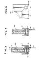
- FIG. 3 - 7 show preferred embodiments according to the present invention in relation to connecting an earthing wire.
- hole 9 is provided through the light-transmissible plate 100, and an earthing wire 15 is connected thereto via metal fitting piece 6a.
- metal fitting piece 6a is fixed by a fixing means, for example, set screw 10a and nut lOb (FIG.3), or a caulking piece 8 (FIG. 4). Then the portion of the connection is covered by a plastic cover 11.
- FIG. 5 shows an embodiment wherein metal fitting piece 6a is fixed nearly parallel to light-transmissible plate 100 in plastic cover 11.
- FIG. 6 shows an embodiment wherein helical insert 12 is fitted into hole 9 and earthing wire 15 is fixed by screw 13 via metal fitting piece 6a.
- providing a hole 11a on the cover 11 facilitates removing the screw 13, and the structure is convenient for removing light-transmissible plate 100 from equipment or cleaning the plate 100.
- FIG. 7 shows an embodiment wherein earthing wire 15 is connected to the plate 100 via adjuster 14a and 14b.
- FIG. 8 is a partial sectional view of a light-transmissible plate having an anti-reflection film constituted by a plurality of layers according to a second embodiment of the present invention.
- hard coating layer 2 On one surface of transparent plastic base plate 1, hard coating layer 2, electroconductive layer 3 and layer 4 having a lower refractive index than the refractive index of electroconductive layer 3 are provided, and on another surface of base plate 1, hard coating layer 2' having scratch resistance and anti-reflection film 20 are provided.
- Anti-reflection film 20 is constructed of No. 1 layer 21, No. 2 layer 22, No. 3 layer 23 and No. 4 layer 24.
- a hard coating layer having scratch resistance is provided on a surface of a transparent plastic base plate.
- a plastic constituting the base plate may be any conventional plastic.
- the transparent base plate means any plastic plate capable of transmitting light. In the case that a light-transmissible plate is used for a display of a word processor etc., it is desirable to apply a base plate set to the transmittance of visible rays of 25 - 70% by its own color or dyeing. The fatigue of the eyes of an operator is reduced by the above restriction.
- the hard coating layer having scratch resistance means a coating layer having high hardness, for example, a layer including polyorganosiloxane, silica or alumina, or a coating layer constructed of a hardening paint, for example, an acrylic the paint.
- the hard coating layer consists of a polyorganosiloxane which is produced by heat-condensing after coating methyltrimethoxysilane and vinyltriethoxysilane or after coating hydrolysis compound thereof. Desirable film thickness of the hard coating layer is in the range of about 1 - 10 ⁇ m.
- the hard coating layer including the acrylic is constructed of, for example, a compound crosslinked with an acrylic compound and an ester compound.
- the acrylic compound is constructed of, for example, methacrylic acid and the ester compound is constructed of, for example, an ester compound produced from an ester and a polyfunctional glycol, for example, pentaerythritol or glycerin.
- an electroconductive layer is provided on a surface of the hard coating layer.
- Any material having electroconductivity and capable of transmitting light can be used for the electroconductive layer, but preferably the layer is constructed of a mixture with indium oxide (In 2 0 3 ) and tin oxide (Sn0 2 ).
- the mixture is also called “ITO” hereinafter in this specification.
- ITO has high electroconductivity, can shield electromagnetic waves effectively and can transmit visible rays.
- a film thickness of the "ITO” layer may be any thickness as long as the layer can satisfy the above functions.
- a desirable thickness is in the range of 100 - 3000 ⁇ (10-300nm) If a thickness of more than 3 00nm is utilized, cracking is liable to occur.
- the " ITO " layer can be coated by sputtering. Other methods can be applied for forming the "ITO” layer.
- the " ITO " layer is formed by evaporation coating using plasma due to high-frequency electric discharge in an atmosphere of oxygen and in a temperature condition of less than 150°C, with the assistance of an ion gun.
- a layer having a lower refractive index than the refractive index of the electroconductive layer is provided on the surface of the electroconductive layer.
- the refractive index of the layer is high.
- the refractive index of the "ITO" layer is about 2.0.
- the layer having the low refractive index may be any conventional low refractive layer, but desirably the layer is a layer including inorganic silica.
- the layer including inorganic silica can be formed by sputtering the silica or by vacuum evaporation coating of the silica.
- the film thickness of the layer may be any thickness as long as the layer can appropriately prevent reflection.
- the hard coating layer, the electroconductive layer and the layer having the low refractive index are provided on one surface of the base plate, or on both surfaces of the base plate. In providing them on one surface; it is preferable to provide at least the hard coating layer on another surface to prevent damage of the another surface, and more preferably, the anti-reflection layer is provided on a surface of the hard coating layer.
- an anti-reflection film composed of a plurality of layers is provided on a surface of the base plate, the surface being an opposite surface to a surface on which the electroconductive layer is provided.
- the anti-reflection film is provided on a surface of the hard coating layer which is provided on one surface of the base plate.
- the film is constructed of No. 1 layer, No. 2 layer, No. 3 layer and No. 4 layer.
- the No. 1 layer is provided on the surface of the hard coating layer.
- the principal ingredient of the No. 1 layer is zirconium oxide.
- the No. 2 layer is provided on the surface of the No. 1 layer, and the principal ingredient of the No. 2 layer is silicon dioxide.
- the No. 1 layer becomes a binder between the hard coating layer and the No. 2 layer, and the strength of both adhesions between the hard coating layer and the No. 1 layer and between the No. 1 layer and the No. 2 layer is increased.
- the No. 1 layer becomes a binder between the hard coating layer and the No. 2 layer, and the strength of both adhesions between the hard coating layer and the No. 1 layer and between the No. 1 layer and the No. 2 layer is increased.
- the equivalent film can be a film having a middle refractive index, compared with the No. 3 layer having a high refractive index and the No. 4 layer having a low refractive index.
- the No. 3 layer is provided on a surface of the No. 2 layer, and the principal ingredient of the No. 3 layer is titanium oxide.
- the No. 4 layer is provided on a surface of the No. 3 layer, and the principal ingredient of the No. 4 layer is silicon dioxide.
- the equivalent film (No. 1 layer and No. 2 layer) having the middle refractive index, the No. 3 layer having the high index and the No. 4 layer having the low index, constitute the anti-reflection film as a whole, with the film having the excellent function of preventing reflection.
- the above anti-reflection film can be coated by vacuum evaporation or sputtering. Vacuum evaporation is better than sputtering. The assistance of an ion beam may be utilized for forming the film. Titanium oxide can be added into the No. 1 layer including zirconium oxide as long as the effect of the present invention is not reduced. In the same manner, Ta205 can be added to the No. 3 layer including titanium oxide.
- the thickness of the anti-reflection film may be any thickness as long as the film can prevent the reflection of visible rays.
- Preferable optical film thicknesses are as follows when the design wave lengtha ⁇ 0 is within 450 - 550 nm.
- the anti-reflection film constructed of a plurality of layers is provided on one surface of the plastic base plate, or on both surfaces of the base plate. In providing the film on one surface, it is desirable to provide the hard coating layer on another surface to prevent i damage of the other surface. It is also provided that the anti-reflection film may be positioned on one surface of the base plate, and that the hard coating layer and indium oxide-tin oxide layer ("ITO" layer), or the layer including silicon dioxide besides them are provided on another surface. In such a light-transmissible plate, a layer having the function of preventing reflection is formed on one surface and a layer having the function of shielding electromagnetic waves is formed on another surface.
- ITO indium oxide-tin oxide layer
- the film thickness of the "ITO” layer is preferably formed to a small size, for example, 100 - 500 ⁇ (10-50nm).
- the film thickness of the "ITO” layer is formed to a large size relatively., for example, 500 - 1000 ⁇ (50-100nm).
- an earthing means may be connected thereto to eliminate static electricity.
- an earthing wire may be connected to the "ITO” layer directly, or continuity via a certain electroconductive piece between the "ITO” layer and the earthing wire may be ensured.
- an outer frame constructed of metal may be provided around the plate, and static electricity may be discharged via the frame.
- the metal frame may preferably come into contact with the "ITO” layer directly, or continuity via a certain electroconductive piece between the metal frame and "ITO" layer may be maintained.
- providing the hard coating layer on the transparent plastic base plate can raise the hardness of the light-transmissible plate, thereby providing characteristics of abrasion resistance and wear resistance to the plate, even if the base plate consists of a plastic having low hardness.
- Providing the electroconductive layer formed on the hard coating layer and the layer having a low refractive index formed on the electroconductive layer can shield electromagnetic waves, and at the same time can prevent reflection.
- the anti-reflection film having excellent static charge resistance is provided on the surface opposite to the surface on which the electroconductive layer is provided, a light-transmissible plate which shields electromagnetic waves can also eliminate static electricity and prevent reflection.
- the anti-reflection film constructed of a plurality of layers also has excellent strength of adhesion, durability, abrasion resistance, wear resistance, shock resistance, chemical resistance, flexibility, heat resistance, light resistance and weather resistance, excellent optical products can be obtained as a whole.
- a representative analysis of components of the electroconductive layer or the anti-reflection film according to the present invention can be carried out by applying Auger electron spectrophotometry.
- Auger electron spectrophotometry an electron beam is irradiated onto a surface of a sample positioned in a high vacuum, and the Auger electron released from the surface is measured by an analyzer with a partition of energy. Conditions of the measurement are as follows.
- the light-transmissible plate shielding electromagnetic waves according to the present invention is effective, particularly when used as a filter for a television set or a display.
- a polymethacrylate plate on the market is used as a transparent plastic base plate.
- the plate is "Acrylite" (trade mark) LN-084, produced by Mitsubishi Rayon Kabushiki Kaisha, colored to gray, thickness; 2 mm.)
- a mixture of two compounds (one is obtained by hydrolyzing vinyltriethoxysilane with glacial acetic acid, another is obtained by hydrolyzing methyltriethoxysilane with glacial acetic acid) is used as a paint for hard coating, as shown in example 1 of Japanese Patent Publication No. SHO 59-114501.
- a paint for the present invention is made by adding sodium acetate, which is a hardener, to the mixture and then by adding a surface lubricant including silicon to the mixture. The paint is coated on a surface of the base plate with thickness of 2 ⁇ m, and it is cured by heating. Thus a hard coating layer is formed.
- a mixture of In 2 0 3 and Sn0 2 is coated on the hard coating layer, and the mixture is coated with film thickness of 700 ⁇ (70nm) by sputtering.
- the condition of the sputtering is at the same condition as shown in example 7 - 9 of Japanese Patent Publication No. SHO 60-32053. That is, the target utilized is indium-tin alloy, a magnetron -sputtering apparatus is used, the atmosphere is a gas mixture of argon and oxygen (oxygen: 30 vol.%), and the vacuum pressure of the atmosphere is 1 x 10⁻³ Torr.
- a film constructed of silicon dioxide is formed on the electroconductive layer.
- the film is formed by electron-beam method, using vacuum evaporation coating apparatus (BMC-800T, produced by Shinku Kikai Kogyo Kabushiki Kaisha).
- the film thickness is 940A (94nm).
- the same hard coating layer as the above is provided on the other surface of the base plate. Then, a film of aluminium oxide and a film of silicon dioxide are formed in order on the hard coating layer, thereby giving a function of hardening the surface and preventing reflection to the plate.
- the light-transmissible plate obtained as above has the following functions. Volume of transmission of electromagnetic waves in the frequency of 10 GHz is reduced to about 1/10 volume, compared with only a transparent plastic base plate. When the plate is used as an optical filter for a word processor, it is excellent with respect to preventing reflection, and fatigue of the eyes of the operator is effectively reduced. Hardness of the surface is increased, thereby the plate is tough against abrasion.
- a hard coating layer on the base plate is formed with the same manner as in example 1.
- a film of o (lOnm) silicon dioxide with thickness of 100A/ is formed as an undercoating layer on the hard coating layer by sputtering.
- "ITO" layer film thickness; 1400 ⁇ (140nm) coated by sputtering and a film of silicon dioxide coated by vacuum evaporation coating are formed in the same manner as in example 1.
- a hard coating layer is formed in the same manner as in example 1.
- layers of Y 2 0 3 ( ⁇ /4), TiO 2 ( ⁇ /2), SIO 2 ( ⁇ /4) are provided in order.
- ⁇ is a design wave length.
- the light-transmissible plate obtained as the above had the following functions.
- the volume of transmission of electromagnetic waves in the frequency of 10 GHz is reduced to about 1/22 volume, compared with only a transparent plastic base plate.
- the plate is used as an optical filter for a word processor, it is more effective with respect to preventing reflection and preventing abrasion than example 1.
- a polymethacrylate plate having a ; hard coating layer thereon, being on the market is used as a base plate.
- the plate is "Acrylite” (trade mark) LN-084, produced by Mitsubishi Rayon Kabushiki Kaisha, colored to gray, thickness; 2 mm.)
- Other layers, that is, the "ITO" layer and a layer having a low refractive index is formed in the same manner as in example 1.
- the plate in the example 3 is manufactured to an excellent plate as well as in example 1.
- a polymethacrylate plate ("Acrylite” (trade mark) LN-084, colored to grey, thickness; 2 mm) is used as a base plate.
- a paint for hard coating a mixture of two compounds (one is obtained by hydrolyzing vinyltriethoxysilane with glacial acetic acid, another is obtained by hydrolyzing methyltriethoxysilane with glacial acetic acid) is used, as shown in example 1 of Japanese Patent Publication No. SHO 59-114501.
- a paint for the present invention was made by adding sodium acetate, which is a hardener, to the mixture, and then by adding surface lubricant including silicon to the mixture.
- the paint is coated on both surfaces of the base plate with a thickness of 2pm, and then it is cured for 3 hours at 90°C. Thus hard coating layers are formed.
- the "ITO” layer is coated on the hard coating layer on one surface of the base plate, and then the SiO 2 layer is provided on the "ITO” layer by vacuum evaporation coating.
- the surface is set in a vacuum evaporation coating tank. After the tank is heated to 60°C and vacuumed to 1 x 10 -5 Torr, the surface is cleaned with an Argon ion beam generated from the ion beam generating device of the Kaofman type, under the acceleration voltage condition of 500 V. Then, the following four layers are formed by electron-beam method, in order, from the surface of the base plate.
- a design wave length in accordance with the optical film thicknesses is 480 nm.
- the plate obtained in the above manner has a reflection interference color of royal purple, and has an extremely excellent function of preventing reflection whereby the surface reflection factor at 550 nm is about 0.2%.
- the plate also has an excellent hardness at the surface.
- An atmospheric exposure test is carried out by exposing the plate outdoors for one month. The result is that there is no break away of the anti-reflection film and no damage of the surface.
- the plate is used as an optical filter for a word processor, it is extremely excellent with respect to preventing reflection, and fatigue of eyes of an operator is highly reduced. Durability of the plate is also excellent.
Landscapes
- Surface Treatment Of Optical Elements (AREA)
- Coating Of Shaped Articles Made Of Macromolecular Substances (AREA)
- Vessels, Lead-In Wires, Accessory Apparatuses For Cathode-Ray Tubes (AREA)
- Devices For Indicating Variable Information By Combining Individual Elements (AREA)
Applications Claiming Priority (2)
| Application Number | Priority Date | Filing Date | Title |
|---|---|---|---|
| JP60084662A JPH0719551B2 (ja) | 1985-04-22 | 1985-04-22 | 電磁波シールド性を有する光学フィルター |
| JP84662/85 | 1985-04-22 |
Publications (3)
| Publication Number | Publication Date |
|---|---|
| EP0200452A2 true EP0200452A2 (de) | 1986-11-05 |
| EP0200452A3 EP0200452A3 (en) | 1989-02-01 |
| EP0200452B1 EP0200452B1 (de) | 1994-07-27 |
Family
ID=13836931
Family Applications (1)
| Application Number | Title | Priority Date | Filing Date |
|---|---|---|---|
| EP86302982A Expired - Lifetime EP0200452B1 (de) | 1985-04-22 | 1986-04-21 | Durchsichtiger elektromagnetischer Schirm |
Country Status (3)
| Country | Link |
|---|---|
| EP (1) | EP0200452B1 (de) |
| JP (1) | JPH0719551B2 (de) |
| DE (1) | DE3689989T2 (de) |
Cited By (14)
| Publication number | Priority date | Publication date | Assignee | Title |
|---|---|---|---|---|
| WO1988002547A1 (en) * | 1986-10-03 | 1988-04-07 | Michael Perander | Display screen with reduced electrostatic field, method and means for making such screen |
| EP0301118A1 (de) * | 1987-07-29 | 1989-02-01 | Walter Lämmler | Strahlungsschwächungselement für Kathodenstrahlröhre |
| DE3935918A1 (de) * | 1988-10-28 | 1990-05-03 | Asahi Optical Co Ltd | Staubdichtes transparentes element |
| EP0372488A3 (de) * | 1988-12-06 | 1991-09-25 | Asahi Glass Company Ltd. | Schirm mit einem antireflexions-Mehrschichtenfilm |
| FR2670981A1 (fr) * | 1990-12-19 | 1992-06-26 | Clausse Georges | Filtre composite a plus de deux surfaces utiles pour ecran de visualisation. |
| EP0277818B1 (de) * | 1987-02-03 | 1993-09-29 | Pilkington Plc | Platte zur elektromagnetischen Abschirmung |
| FR2690041A1 (fr) * | 1992-04-14 | 1993-10-15 | Clausse Georges | Cadre en blindage contre les champs électromagnétiques émis par les tubes cathodiques. |
| FR2696277A1 (fr) * | 1992-09-25 | 1994-04-01 | Thomson Csf | Dispositif de visualisation à écran de faible rayonnement compromettant. |
| EP0753762A1 (de) * | 1995-07-06 | 1997-01-15 | Sony Corporation | Elektrisch leitender, Antireflektionsbelag |
| EP0841680A1 (de) * | 1996-11-11 | 1998-05-13 | Sony Corporation | Explosionssicher Folie und Kathodenstrahlröhre |
| WO1998032152A1 (en) * | 1997-01-17 | 1998-07-23 | Koninklijke Philips Electronics N.V. | Method of manufacturing a cathode ray tube and a cathode ray tube |
| US5874801A (en) * | 1995-09-14 | 1999-02-23 | Sony Corporation | Anti-reflection member, manufacturing method thereof, and cathode-ray tube |
| US6686031B2 (en) * | 2000-02-23 | 2004-02-03 | Fuji Photo Film Co., Ltd. | Hard coat film and display device having same |
| US6784608B2 (en) * | 1999-12-22 | 2004-08-31 | Sony Corporation | Light-absorptive antireflection filter, with pigment containing light-absorptive film and electroconducting thin film, and device using same |
Families Citing this family (8)
| Publication number | Priority date | Publication date | Assignee | Title |
|---|---|---|---|---|
| JPH0637361Y2 (ja) * | 1987-03-02 | 1994-09-28 | 東レ株式会社 | 除電性を有する多層反射防止光透過板 |
| JPS63280790A (ja) * | 1987-05-13 | 1988-11-17 | Toray Ind Inc | 帯電防止物品 |
| DE69130921T2 (de) * | 1990-11-21 | 1999-06-24 | Catalysts & Chemicals Industries Co., Ltd., Tokio/Tokyo | Überzugslösung zur bildung eines durchsichtigen, leitfähigen films, verfahren zu deren herstellung, leitfähiges substrat, verfahren zur dessen herstellung, und anzeigevorrichtung mit einem durchsichtigen, leitfähigen substrat |
| JPH06130202A (ja) * | 1992-10-15 | 1994-05-13 | Toray Ind Inc | 光学用耐熱樹脂板 |
| TW417025B (en) | 1997-04-10 | 2001-01-01 | Sumitomo Chemical Co | Front plate for plasma display |
| KR100735176B1 (ko) | 2000-04-28 | 2007-07-03 | 엘지전자 주식회사 | 칼라 음극선관의 스크린 구조체 |
| WO2011122152A1 (ja) * | 2010-03-30 | 2011-10-06 | 日本電気硝子株式会社 | 電磁波遮蔽膜及び電磁波遮蔽部材 |
| JP6251899B1 (ja) | 2017-03-31 | 2017-12-27 | グンゼ株式会社 | 反射防止フィルム |
Family Cites Families (13)
| Publication number | Priority date | Publication date | Assignee | Title |
|---|---|---|---|---|
| US3760215A (en) * | 1972-08-22 | 1973-09-18 | Us Navy | Low-reflection filter for cathode ray tube face plate |
| JPS542820B2 (de) * | 1972-11-18 | 1979-02-14 | ||
| US3984581A (en) * | 1973-02-28 | 1976-10-05 | Carl Zeiss-Stiftung | Method for the production of anti-reflection coatings on optical elements made of transparent organic polymers |
| US4128303A (en) * | 1976-04-05 | 1978-12-05 | Kabushiki Kaisha Hoya Lens | Anti reflection coating with a composite middle layer |
| JPS53147549A (en) * | 1977-05-30 | 1978-12-22 | Toshiba Corp | Forming method of antireflection film |
| US4246613A (en) * | 1979-01-10 | 1981-01-20 | Delta Data Systems Corporation | Anti-glare screen with electromagnetic interference rejection |
| US4381421A (en) * | 1980-07-01 | 1983-04-26 | Tektronix, Inc. | Electromagnetic shield for electronic equipment |
| JPS57204002A (en) * | 1981-06-10 | 1982-12-14 | Toray Ind Inc | Plastic filter for luminous displaying |
| US4433247A (en) * | 1981-09-28 | 1984-02-21 | Varian Associates, Inc. | Beam sharing method and apparatus for ion implantation |
| JPS58209549A (ja) * | 1982-06-01 | 1983-12-06 | 株式会社豊田中央研究所 | 熱線しゃへい積層体 |
| US4422721A (en) * | 1982-08-09 | 1983-12-27 | Optical Coating Laboratory, Inc. | Optical article having a conductive anti-reflection coating |
| DE3430406A1 (de) * | 1983-08-20 | 1985-03-14 | Riken EMC Co., Ltd., Nagoya, Aichi | Transparente platte fuer optische zeichenwiedergabevorrichtung |
| EP0145201A1 (de) * | 1983-11-10 | 1985-06-19 | Optical Coating Laboratory, Inc. | Antireflektive optische Beschichtung mit antistatischen Eigenschaften |
-
1985
- 1985-04-22 JP JP60084662A patent/JPH0719551B2/ja not_active Expired - Fee Related
-
1986
- 1986-04-21 DE DE3689989T patent/DE3689989T2/de not_active Expired - Fee Related
- 1986-04-21 EP EP86302982A patent/EP0200452B1/de not_active Expired - Lifetime
Cited By (15)
| Publication number | Priority date | Publication date | Assignee | Title |
|---|---|---|---|---|
| WO1988002547A1 (en) * | 1986-10-03 | 1988-04-07 | Michael Perander | Display screen with reduced electrostatic field, method and means for making such screen |
| EP0277818B1 (de) * | 1987-02-03 | 1993-09-29 | Pilkington Plc | Platte zur elektromagnetischen Abschirmung |
| EP0301118A1 (de) * | 1987-07-29 | 1989-02-01 | Walter Lämmler | Strahlungsschwächungselement für Kathodenstrahlröhre |
| DE3935918A1 (de) * | 1988-10-28 | 1990-05-03 | Asahi Optical Co Ltd | Staubdichtes transparentes element |
| EP0372488A3 (de) * | 1988-12-06 | 1991-09-25 | Asahi Glass Company Ltd. | Schirm mit einem antireflexions-Mehrschichtenfilm |
| FR2670981A1 (fr) * | 1990-12-19 | 1992-06-26 | Clausse Georges | Filtre composite a plus de deux surfaces utiles pour ecran de visualisation. |
| FR2690041A1 (fr) * | 1992-04-14 | 1993-10-15 | Clausse Georges | Cadre en blindage contre les champs électromagnétiques émis par les tubes cathodiques. |
| FR2696277A1 (fr) * | 1992-09-25 | 1994-04-01 | Thomson Csf | Dispositif de visualisation à écran de faible rayonnement compromettant. |
| EP0753762A1 (de) * | 1995-07-06 | 1997-01-15 | Sony Corporation | Elektrisch leitender, Antireflektionsbelag |
| US5874801A (en) * | 1995-09-14 | 1999-02-23 | Sony Corporation | Anti-reflection member, manufacturing method thereof, and cathode-ray tube |
| EP0841680A1 (de) * | 1996-11-11 | 1998-05-13 | Sony Corporation | Explosionssicher Folie und Kathodenstrahlröhre |
| US6111352A (en) * | 1996-11-11 | 2000-08-29 | Sony Corporation | Explosion-proof film and cathode-ray tube |
| WO1998032152A1 (en) * | 1997-01-17 | 1998-07-23 | Koninklijke Philips Electronics N.V. | Method of manufacturing a cathode ray tube and a cathode ray tube |
| US6784608B2 (en) * | 1999-12-22 | 2004-08-31 | Sony Corporation | Light-absorptive antireflection filter, with pigment containing light-absorptive film and electroconducting thin film, and device using same |
| US6686031B2 (en) * | 2000-02-23 | 2004-02-03 | Fuji Photo Film Co., Ltd. | Hard coat film and display device having same |
Also Published As
| Publication number | Publication date |
|---|---|
| EP0200452A3 (en) | 1989-02-01 |
| JPH0719551B2 (ja) | 1995-03-06 |
| EP0200452B1 (de) | 1994-07-27 |
| DE3689989D1 (de) | 1994-09-01 |
| JPS61245449A (ja) | 1986-10-31 |
| DE3689989T2 (de) | 1995-02-09 |
Similar Documents
| Publication | Publication Date | Title |
|---|---|---|
| US4732454A (en) | Light-transmissible plate shielding electromagnetic waves | |
| EP0200452A2 (de) | Durchsichtiger elektromagnetischer Schirm | |
| US4804883A (en) | Front attachment for CRT. E.G. for a monitor or video tube | |
| US6313577B1 (en) | Optical articles and cathode-ray tube using the same | |
| EP0145201A1 (de) | Antireflektive optische Beschichtung mit antistatischen Eigenschaften | |
| EP0679288B1 (de) | Reflexionsfreie und antistatische beschichtung für eine kathodenstrahlröhre | |
| JPH1173119A (ja) | 電磁波シールド効果を有する反射防止コート及び反射防止コートを有する光学部材 | |
| JPH0746570B2 (ja) | 電磁波シ−ルド性を有する光透過板 | |
| KR100363770B1 (ko) | 비디오디스플레이패널의정전기방지및반사방지코팅 | |
| US6171457B1 (en) | Method of fabricating low resistance, anti-reflection CRT | |
| JP3223261B2 (ja) | 陰極線管およびその製造方法 | |
| JPH0789597B2 (ja) | 電磁波シ−ルド性を有する光透過板 | |
| US7655280B2 (en) | Extreme low resistivity light attenuation anti-reflection coating structure and method for manufacturing the same | |
| JPH09197102A (ja) | 多層反射防止膜を有するプラスティック製光学物品 | |
| JPH0685001B2 (ja) | 多層反射防止膜を有する光学物品 | |
| JPH0637361Y2 (ja) | 除電性を有する多層反射防止光透過板 | |
| JP3072991B2 (ja) | 陰極線管 | |
| KR19980703086A (ko) | 다층 반사 방지 필름을 가진 플라스틱 광학 물품 | |
| JPH09197103A (ja) | 多層反射防止膜を有するプラスティック製光学物品 | |
| EP0894331B1 (de) | Verfahren zur Herstellung einer Kathodenstrahlröhre | |
| JP2006289901A (ja) | 反射防止フィルムおよびディスプレイ装置 | |
| JP3541606B2 (ja) | 低反射樹脂基材 | |
| US7785714B2 (en) | Extreme low resistivity light attenuation anti-reflection coating structure and method for manufacturing the same | |
| JP2002221601A (ja) | 反射防止積層体 | |
| JPH11149063A (ja) | 反射防止膜付き眼鏡レンズ |
Legal Events
| Date | Code | Title | Description |
|---|---|---|---|
| PUAI | Public reference made under article 153(3) epc to a published international application that has entered the european phase |
Free format text: ORIGINAL CODE: 0009012 |
|
| AK | Designated contracting states |
Kind code of ref document: A2 Designated state(s): DE FR GB IT NL |
|
| PUAL | Search report despatched |
Free format text: ORIGINAL CODE: 0009013 |
|
| AK | Designated contracting states |
Kind code of ref document: A3 Designated state(s): DE FR GB IT NL |
|
| 17P | Request for examination filed |
Effective date: 19890429 |
|
| 17Q | First examination report despatched |
Effective date: 19910320 |
|
| GRAA | (expected) grant |
Free format text: ORIGINAL CODE: 0009210 |
|
| RBV | Designated contracting states (corrected) |
Designated state(s): DE GB |
|
| AK | Designated contracting states |
Kind code of ref document: B1 Designated state(s): DE GB |
|
| REF | Corresponds to: |
Ref document number: 3689989 Country of ref document: DE Date of ref document: 19940901 |
|
| PLBE | No opposition filed within time limit |
Free format text: ORIGINAL CODE: 0009261 |
|
| STAA | Information on the status of an ep patent application or granted ep patent |
Free format text: STATUS: NO OPPOSITION FILED WITHIN TIME LIMIT |
|
| 26N | No opposition filed | ||
| PGFP | Annual fee paid to national office [announced via postgrant information from national office to epo] |
Ref country code: GB Payment date: 20010418 Year of fee payment: 16 Ref country code: DE Payment date: 20010418 Year of fee payment: 16 |
|
| REG | Reference to a national code |
Ref country code: GB Ref legal event code: IF02 |
|
| PG25 | Lapsed in a contracting state [announced via postgrant information from national office to epo] |
Ref country code: GB Free format text: LAPSE BECAUSE OF NON-PAYMENT OF DUE FEES Effective date: 20020421 |
|
| PG25 | Lapsed in a contracting state [announced via postgrant information from national office to epo] |
Ref country code: DE Free format text: LAPSE BECAUSE OF NON-PAYMENT OF DUE FEES Effective date: 20021101 |
|
| GBPC | Gb: european patent ceased through non-payment of renewal fee |
Effective date: 20020421 |