EP0200427A1 - Elektrooptische Vorrichtung mit chiral smektischem Flüssigkristall und Verfahren zu deren Ansteuerung - Google Patents
Elektrooptische Vorrichtung mit chiral smektischem Flüssigkristall und Verfahren zu deren Ansteuerung Download PDFInfo
- Publication number
- EP0200427A1 EP0200427A1 EP19860302887 EP86302887A EP0200427A1 EP 0200427 A1 EP0200427 A1 EP 0200427A1 EP 19860302887 EP19860302887 EP 19860302887 EP 86302887 A EP86302887 A EP 86302887A EP 0200427 A1 EP0200427 A1 EP 0200427A1
- Authority
- EP
- European Patent Office
- Prior art keywords
- liquid crystal
- state
- voltage
- crystal molecules
- chiral smectic
- Prior art date
- Legal status (The legal status is an assumption and is not a legal conclusion. Google has not performed a legal analysis and makes no representation as to the accuracy of the status listed.)
- Granted
Links
Images


Classifications
-
- G—PHYSICS
- G09—EDUCATION; CRYPTOGRAPHY; DISPLAY; ADVERTISING; SEALS
- G09G—ARRANGEMENTS OR CIRCUITS FOR CONTROL OF INDICATING DEVICES USING STATIC MEANS TO PRESENT VARIABLE INFORMATION
- G09G3/00—Control arrangements or circuits, of interest only in connection with visual indicators other than cathode-ray tubes
- G09G3/20—Control arrangements or circuits, of interest only in connection with visual indicators other than cathode-ray tubes for presentation of an assembly of a number of characters, e.g. a page, by composing the assembly by combination of individual elements arranged in a matrix no fixed position being assigned to or needed to be assigned to the individual characters or partial characters
- G09G3/34—Control arrangements or circuits, of interest only in connection with visual indicators other than cathode-ray tubes for presentation of an assembly of a number of characters, e.g. a page, by composing the assembly by combination of individual elements arranged in a matrix no fixed position being assigned to or needed to be assigned to the individual characters or partial characters by control of light from an independent source
- G09G3/36—Control arrangements or circuits, of interest only in connection with visual indicators other than cathode-ray tubes for presentation of an assembly of a number of characters, e.g. a page, by composing the assembly by combination of individual elements arranged in a matrix no fixed position being assigned to or needed to be assigned to the individual characters or partial characters by control of light from an independent source using liquid crystals
- G09G3/3611—Control of matrices with row and column drivers
- G09G3/3622—Control of matrices with row and column drivers using a passive matrix
- G09G3/3629—Control of matrices with row and column drivers using a passive matrix using liquid crystals having memory effects, e.g. ferroelectric liquid crystals
-
- G—PHYSICS
- G09—EDUCATION; CRYPTOGRAPHY; DISPLAY; ADVERTISING; SEALS
- G09G—ARRANGEMENTS OR CIRCUITS FOR CONTROL OF INDICATING DEVICES USING STATIC MEANS TO PRESENT VARIABLE INFORMATION
- G09G2310/00—Command of the display device
- G09G2310/06—Details of flat display driving waveforms
-
- G—PHYSICS
- G09—EDUCATION; CRYPTOGRAPHY; DISPLAY; ADVERTISING; SEALS
- G09G—ARRANGEMENTS OR CIRCUITS FOR CONTROL OF INDICATING DEVICES USING STATIC MEANS TO PRESENT VARIABLE INFORMATION
- G09G2310/00—Command of the display device
- G09G2310/06—Details of flat display driving waveforms
- G09G2310/061—Details of flat display driving waveforms for resetting or blanking
-
- G—PHYSICS
- G09—EDUCATION; CRYPTOGRAPHY; DISPLAY; ADVERTISING; SEALS
- G09G—ARRANGEMENTS OR CIRCUITS FOR CONTROL OF INDICATING DEVICES USING STATIC MEANS TO PRESENT VARIABLE INFORMATION
- G09G3/00—Control arrangements or circuits, of interest only in connection with visual indicators other than cathode-ray tubes
- G09G3/20—Control arrangements or circuits, of interest only in connection with visual indicators other than cathode-ray tubes for presentation of an assembly of a number of characters, e.g. a page, by composing the assembly by combination of individual elements arranged in a matrix no fixed position being assigned to or needed to be assigned to the individual characters or partial characters
- G09G3/2007—Display of intermediate tones
- G09G3/2014—Display of intermediate tones by modulation of the duration of a single pulse during which the logic level remains constant
Definitions
- This invention relates to chiral smectic liquid crystal electro-optical devices and methods of driving same.
- liquid crystal devices using a chiral smectic C-phase liquid crystal material have attracted attention. Such devices are used as optical shutters in display devices, cameras and printers that operate at high speeds and have memory retentivity.
- a widely known example of a ferrosfectric liquid crystal compound having the chiral smectic C-phase is a 2-methytbutylP-(P-n-decytoxyben- zylidene)amino)-
- the liquid crystal molecules are arranged in a spiral structure being twisted in each of layers L,, L 2 , L j , L. ( Figure 8) by a given azimuthal angle ⁇ .
- the other domain has a downwardly directed electric dipole moment. If an electric field is applied between the substrates B, B', all of the liquid crystal molecules are orientated at positions tilted by either + ⁇ or -0 from the direction normal to the layer. Further, if the electric field is applied in the opposite direct, the liquid crystal molecules are inverted and are orientated at positions tilted by either - 0 or + ⁇ .
- the liquid crystal panel thus constituted exhibits excellent characteristics, i.e. has a remarkably high response speed of the order of microseconds and retains displayed information even after the electric field has been removed.
- the above memory retentivity is very advantageous from the standpoint of reducing electric power consumption.
- writing of the dark condition and that of the bright condition must be effectsd by separate frame scannings. Namely, an extended period of time is required for changing display information.
- the present invention seeks to provide a chiral smectic liquid crystal electro-optical device which is capable of effecting writing of bright and dark conditions in a single scanning frame at relatively high speed.
- a chiral smectic liquid crystal electro-optical device which uses switctrang between two states of chiral smectic liquid crystal molecules characterised by means for driving the device by utilising the difference between response time from one of said two states to the other state and the response time from the other state to the one state.
- said means are such that the change from said one state to said other state is performed by applying an AC voltage having an amplitude and a pulse width which may change the liquid crystal molecules from said one state to said other state but may not change from said other state to said one state, and the change to said one state is performed by applying an AC voltage having an amplitude and pulse width which may change the liquid crystal molecules from said state to said other state and from said other state to said one state.
- the amplitude of the AC voltage may be constant.
- the pulse width of the AC voltage may be constant.
- a method of driving a chiral smectic liquid crystal electro-optical device which uses switching between two states of chiral smectic liquid crystal molecules characterised by utilising the difference between the response time from one of said two states to the other state and the response time from the other state to the one state.
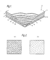
- a substrate 1 which constitutes a liquid crystal display panel is composed of a random horizontally orientated layer 1 that is uniformally orientated in all directions.
- the layer 1 c is formed, e.g. by printing or dipping, of a thin polyimide film on the surface of an electrically insulating transparent plate 1 made of, e.g. glass on which are formed segment electrodes 1a, composed of transparent conductive material ( Figure 2(a)).
- a second substrate 2 which together with the substrate 1 constitutes a liquid crystal display panel has a mono-axially orientated layer 2c.
- the layer 2c is obtained by forming a thin polyimide film on the surface of an electrically insulating transparent plate 2b on which are formed common electrodes 2a which are at right angles to the electrodes 1 a.
- the surface of this thin polyimide film is rubbed in one direction so as to be orientated only in one direction ( Figure 2(b)).
- These two substrates 1 and 2 are disposed so as to be parallel to one another with a gap therebetween.
- the gap is smaller than the spiral pitch of a ferro-electric chiral smectic liquid crystal compound 3.
- the random horizontally orientated layer 1c and the monoaxially orientated layer 2c are opposed to each other.
- the space between the two substrates 1, 2 is filled with a ferro-electric chiral smectic liquid crystal compound 3 obtained by mixing an S-4-0 (2-methyl)-butyl-resorcylidene-4-alkyln-octylaniline and a P-n-octylphenyl-P'-6-methyloctyloxybenzoate in equal amounts.
- the peripheries of the substrates are sealed with a sealing agent to form a cellular structure, thereby to constitute a display panel 6.
- reference numerals 4,5 denote polarising plates that are placed on the outer surfaces of the substrates 1,2 respectively.
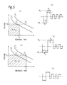
- a voltage is applied to the electrodes of the thus-constructed liquid crystal panel to examine the inversion speed of the domains.
- a voltage of the same level is applied as shown in Figure 3
- the speed r, at which the bright condition changes to the dark condition is different from the speed ⁇ 2 at which the dark condition changes into the bright condition. Namely, there is a difference ⁇ ⁇ in the response time between the two.
- the present invention seeks to effect writing of the bright condition and that of the dark condition simultaneously by fully utilising the time difference ⁇ ⁇ when the display conditions are switched.
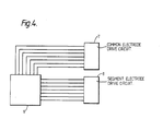
- Figure 4 illustrates an embodiment of a drive circuit for the display panel 6 of Figure 1.
- the drive circuit has a common electrode drive circuit 7 connected to the common electrodes 2a of the display panel 6, and a segment electrode drive circuit 8 connected to the segment electrode 1a.
- a common electrode drive circuit 7 connected to the common electrodes 2a of the display panel 6, and a segment electrode drive circuit 8 connected to the segment electrode 1a.
- the drive circuit selectively produces:
- the liquid crystal molecules contained in the narrow gat between the substrates 1,2 are captured at one end by the random horizontally orientated layer 1c.
- the liquid crystal molecules however, have freedom in the direction of the plane. Therefore, the other ends of the liquid crystal molecules are biased in one direction by the monoaxially orientated layer 2c. Namely, all of the liquid crystal molecules held between the substrates 1,2 are arranged in one direction and maintain a uniform optical density over the whole surface to form a uniform background without developing any pattern.
- the liquid crystal molecules of selected picture elements are affected by the electric field for a period of time longer than the inversion time ⁇ 1 at the voltage -V, of the pulse P, but shorter than the inversion time T2 , and are sufficiently inverted into the dark condition.
- the pulse P z is applied after the inversion, the liquid crystal molecules of the selected picture elements are not inverted into the bright condition since the interval T, of the pulse P z is shorter than the time T2 for changing the dark condition into the bright condition. Therefore, the dark condition is maintained, i.e. write condition of the pulse P, is maintained. Due to the maintenance signal applied after the write signal, the liquid crystal molecules of the selected picture elements are dynamically maintained in the dark condition.
- the liquid crystal molecules of the selected picture elements are affected by the electric field for the period of time T 2 which is longer than the inversion time at the voltage -V, of the pulse P 3 and temporarily change into the dark condition.
- the pulse P 4 that is applied subsequently has the interval T z which is longer than the inversion time T2 for inverting the dark condition into the bright condition at the voltage V, the liquid crystal molecules are inverted from the dark condition written by the pulse P3, and write the bright condition. Due to the maintenance signal applied after the write signal, the liquid crystal molecules of the selected picture elements are dynamically maintained in the bright condition.
- the writing of the dark condition and that of the bright condition can be effected at a high speed of the order of several hundreds of microseconds. It will be appreciated that, in the above mentioned step, the liquid crystal molecules alternately are affected by voltages having the same voltage level and the same interval. Therefore, the picture elements are free from any residual electric charge.
- either the first mode signal or the second mode signal is selected depending upon the condition that is to be written, and the dark condition and the bright condition can be written by one- frame scanning.
- the displayed information is maintained by applying an AC voltage having a peak value which is 1/N of the drive voltage after the pattern is displayed.
- an AC voltage having a peak value which is 1/N of the drive voltage after the pattern is displayed.
- the liquid crystal molecules are captured in a new axis of orientation in the random horizontally orientated layer 1 c, directions of the liquid crystal molecules are maintained even after the application of the AC voltage is discontinued, so that the displayed information can be stored.
- the first mode signal is used for writing the dark condition and the second mode signal is used for writing the bright condition.
- they can be suitably interchanged depending upon the operation characteristics of the liquid crystal panel.
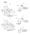
- Figure 6 shows a second embodiment of a display device according to the present invention which produces a graduation display by utilising changes in the concentration of picture elements relative to the time for applying the electric field as shown in Figure 7.
- the device applies:
- the liquid crystal molecules of the selected picture elements change to the dark condition - ( Figure 7) at a concentration proportional to the volgate -V, of the pulse P s and the interval Tx. If the pulse P 6 is applied under this condition, the liquid crystal molecules cannot migrate to positions corresponding to the dark condition and maintain the concentration position written by the pulse P s , since the interval Ty of the peak voltage V, is shorter than the inversion time ⁇ 2 for inverting the dark condition into the bright condition. Due to the maintenance signal applied after the write signal, the liquid crystal molecules dynamically maintain the displayed concentration around the selected positions.
- the liquid crystal molecules temporarily change into the dark condition, since the interval Ty of the pulse P, is longer than the inversion time T2 .
- the pulse P s which is subsequently applied has the interval Ty which is sufficient to migrate the liquid crystal molecules from the dark condition to the bright condition, the liquid crystal molecules migrate from the dark condition written by the pulse P7 to the bright condition, and write brightness which is proportional to the interval Ty. Therefore, it is possible to write information having graduation at a very high speed of the order of several hundreds of microseconds in one step.
- graduation is provided for both in the dark condition and the bright condition. It will, however, be appreciated that the same effect can be produced even when graduation is provided for in either one of these conditions, for example, for writing the dark condition.
- the selecting pulses P, to P a have a constant amplitude and have different pulse widths T,, T z , T x , Ty in order to utilise the difference between the response time from one of the two states to the other state and the response time from the other state to the one state for driving.
- selecting pulses which have a constant pulse width and have different amplitude between the case of ON to OFF and the case of OFF to ON.
- ferro-electric smectic liquid crystal compound it is also possible to use a chiral smectic liquid crystal compound such as a pyrimide-type liquid crystal compound represented by the general formula: or 2-methylbutyl p-(P-n-decyloxybenzilidene)-amino ⁇ , etc.
- a chiral smectic liquid crystal compound such as a pyrimide-type liquid crystal compound represented by the general formula: or 2-methylbutyl p-(P-n-decyloxybenzilidene)-amino ⁇ , etc.
- the monoaxially orientated layer and the random horizontally orientated layer composed of polyimide were formed on the surfaces of the substrates.
- the monoaxially orientated film may be composed of an organic material such as polyvinyl alcohol, fluororesin or silane, or an obliquely deposited Si02 film in addition to the polyimide.
- the random horizontally orientated film on the other substrate may be composed of organic material such as epoxy, polyvinyl alcohol, fluororesin, polyurethane, silane, phenol or urea, or an inorganic film formed by depositing vapours of Si02 or MgF z in addition to the polyimide.
- a monoaxially alignment treatment is given and on the other inner surface of the other a random homogeneous alignment treatment is given.
- These treatments are proper in the case of using the liquid crystal compounds mentioned above.
- other smectic liquid crystal compounds it may be proper that both of the inner surfaces of the two substrates are treated to produce monoaxial alignment.
- the liquid crystal panel comprising a smectic liquid crystal compound is affected by a write signal consisting of an AC signal having an interval ranging from the first inversion time to the second inversion time of the liquid crystal compound and an AC signal having an interval greater than one of said two inversion times whichever is the longer. Therefore, the bright and dark conditions can be written within a period of one frame of scanning maintaining memory retentivity and uniform background. Thus, it is possible to realise a display device such as an optical shutter which effects the scanning at high speed.
Landscapes
- Engineering & Computer Science (AREA)
- Chemical & Material Sciences (AREA)
- Crystallography & Structural Chemistry (AREA)
- Physics & Mathematics (AREA)
- Computer Hardware Design (AREA)
- General Physics & Mathematics (AREA)
- Theoretical Computer Science (AREA)
- Liquid Crystal (AREA)
- Liquid Crystal Display Device Control (AREA)
- Devices For Indicating Variable Information By Combining Individual Elements (AREA)
Applications Claiming Priority (2)
| Application Number | Priority Date | Filing Date | Title |
|---|---|---|---|
| JP8365185A JPS61241731A (ja) | 1985-04-19 | 1985-04-19 | スメクテイック液晶装置 |
| JP83651/85 | 1985-04-19 |
Publications (2)
| Publication Number | Publication Date |
|---|---|
| EP0200427A1 true EP0200427A1 (de) | 1986-11-05 |
| EP0200427B1 EP0200427B1 (de) | 1991-11-27 |
Family
ID=13808352
Family Applications (1)
| Application Number | Title | Priority Date | Filing Date |
|---|---|---|---|
| EP19860302887 Expired - Lifetime EP0200427B1 (de) | 1985-04-19 | 1986-04-17 | Elektrooptische Vorrichtung mit chiral smektischem Flüssigkristall und Verfahren zu deren Ansteuerung |
Country Status (3)
| Country | Link |
|---|---|
| EP (1) | EP0200427B1 (de) |
| JP (1) | JPS61241731A (de) |
| DE (1) | DE3682610D1 (de) |
Cited By (1)
| Publication number | Priority date | Publication date | Assignee | Title |
|---|---|---|---|---|
| EP0300754A2 (de) * | 1987-07-21 | 1989-01-25 | THORN EMI plc | Anzeigegerät |
Families Citing this family (3)
| Publication number | Priority date | Publication date | Assignee | Title |
|---|---|---|---|---|
| US4836656A (en) * | 1985-12-25 | 1989-06-06 | Canon Kabushiki Kaisha | Driving method for optical modulation device |
| US5255110A (en) * | 1985-12-25 | 1993-10-19 | Canon Kabushiki Kaisha | Driving method for optical modulation device using ferroelectric liquid crystal |
| JPH061310B2 (ja) * | 1987-05-13 | 1994-01-05 | キヤノン株式会社 | 液晶装置 |
Citations (4)
| Publication number | Priority date | Publication date | Assignee | Title |
|---|---|---|---|---|
| EP0106386A2 (de) * | 1982-09-23 | 1984-04-25 | BBC Brown Boveri AG | Verfahren zur Ansteuerung einer multiplexierbaren, bistabilen Flüssigkristallanzeige |
| DE3414704A1 (de) * | 1983-04-19 | 1984-10-25 | Canon K.K., Tokio/Tokyo | Verfahren zum ansteuern einer optischen moduliervorrichtung |
| US4508429A (en) * | 1982-04-16 | 1985-04-02 | Hitachi, Ltd. | Method for driving liquid crystal element employing ferroelectric liquid crystal |
| EP0149899A2 (de) * | 1983-12-09 | 1985-07-31 | Seiko Instruments Inc. | Flüssigkristallanzeigeeinrichtung |
-
1985
- 1985-04-19 JP JP8365185A patent/JPS61241731A/ja active Granted
-
1986
- 1986-04-17 DE DE8686302887T patent/DE3682610D1/de not_active Expired - Fee Related
- 1986-04-17 EP EP19860302887 patent/EP0200427B1/de not_active Expired - Lifetime
Patent Citations (4)
| Publication number | Priority date | Publication date | Assignee | Title |
|---|---|---|---|---|
| US4508429A (en) * | 1982-04-16 | 1985-04-02 | Hitachi, Ltd. | Method for driving liquid crystal element employing ferroelectric liquid crystal |
| EP0106386A2 (de) * | 1982-09-23 | 1984-04-25 | BBC Brown Boveri AG | Verfahren zur Ansteuerung einer multiplexierbaren, bistabilen Flüssigkristallanzeige |
| DE3414704A1 (de) * | 1983-04-19 | 1984-10-25 | Canon K.K., Tokio/Tokyo | Verfahren zum ansteuern einer optischen moduliervorrichtung |
| EP0149899A2 (de) * | 1983-12-09 | 1985-07-31 | Seiko Instruments Inc. | Flüssigkristallanzeigeeinrichtung |
Cited By (2)
| Publication number | Priority date | Publication date | Assignee | Title |
|---|---|---|---|---|
| EP0300754A2 (de) * | 1987-07-21 | 1989-01-25 | THORN EMI plc | Anzeigegerät |
| EP0300754A3 (en) * | 1987-07-21 | 1990-06-13 | Thorn Emi Plc | Display device |
Also Published As
| Publication number | Publication date |
|---|---|
| EP0200427B1 (de) | 1991-11-27 |
| JPH0431372B2 (de) | 1992-05-26 |
| JPS61241731A (ja) | 1986-10-28 |
| DE3682610D1 (de) | 1992-01-09 |
Similar Documents
| Publication | Publication Date | Title |
|---|---|---|
| JP3427611B2 (ja) | 液晶表示装置 | |
| EP0168242A2 (de) | Elektrooptische Vorrichtung mit einem ferroelektrischen Flüssigkristall | |
| US7123330B2 (en) | Liquid crystal panel substrate having alignment film and method for forming alignment film by varied evaporation angle | |
| EP0200427A1 (de) | Elektrooptische Vorrichtung mit chiral smektischem Flüssigkristall und Verfahren zu deren Ansteuerung | |
| JPS61166590A (ja) | 液晶表示素子及びその駆動方法 | |
| JPS62275223A (ja) | 液晶素子及びその駆動法 | |
| JPS60235121A (ja) | 液晶素子の駆動方法 | |
| JPS6230224A (ja) | スメクテイツク液晶装置 | |
| JPS60263124A (ja) | 液晶素子の駆動方法 | |
| JP2789602B2 (ja) | アクティブマトリクス装置及びその駆動方法 | |
| JP2006251612A (ja) | 表示媒体とそれを用いた表示装置及び可逆表示体 | |
| KR100477132B1 (ko) | 강유전성 액정 물질을 사용하는 액정 표시 장치의 제조 방법 | |
| JPH09311315A (ja) | 強誘電性液晶素子および強誘電性液晶材料 | |
| JPS60217336A (ja) | 液晶表示装置 | |
| JPS60262136A (ja) | 液晶素子の駆動法 | |
| US4012121A (en) | Texture transformations in optically negative liquid crystals | |
| JPS6256933A (ja) | 液晶マトリツクス表示パネルの駆動法 | |
| JP3230754B2 (ja) | 液晶表示装置 | |
| JPH02126226A (ja) | 液晶電気光学素子 | |
| JPS6126024A (ja) | 液晶多色表示装置 | |
| JPS6210628A (ja) | 液晶電気光学装置 | |
| JPS62231934A (ja) | 光学変調素子 | |
| JPS62235930A (ja) | 強誘電性液晶素子の駆動法 | |
| JPS6348529A (ja) | 液晶素子の駆動方法 | |
| JPS60262135A (ja) | 液晶素子の駆動法 |
Legal Events
| Date | Code | Title | Description |
|---|---|---|---|
| PUAI | Public reference made under article 153(3) epc to a published international application that has entered the european phase |
Free format text: ORIGINAL CODE: 0009012 |
|
| AK | Designated contracting states |
Kind code of ref document: A1 Designated state(s): DE FR GB IT SE |
|
| PUAB | Information related to the publication of an a document modified or deleted |
Free format text: ORIGINAL CODE: 0009199EPPU |
|
| PUAF | Information related to the publication of a search report (a3 document) modified or deleted |
Free format text: ORIGINAL CODE: 0009199SEPU |
|
| R17D | Deferred search report published (corrected) |
Effective date: 19861210 |
|
| RA1 | Application published (corrected) |
Date of ref document: 19861210 Kind code of ref document: A1 |
|
| 17P | Request for examination filed |
Effective date: 19870501 |
|
| RAP1 | Party data changed (applicant data changed or rights of an application transferred) |
Owner name: SEIKO INSTRUMENTS INC. |
|
| 17Q | First examination report despatched |
Effective date: 19890803 |
|
| GRAA | (expected) grant |
Free format text: ORIGINAL CODE: 0009210 |
|
| AK | Designated contracting states |
Kind code of ref document: B1 Designated state(s): DE FR GB IT SE |
|
| PG25 | Lapsed in a contracting state [announced via postgrant information from national office to epo] |
Ref country code: SE Effective date: 19911127 |
|
| ITF | It: translation for a ep patent filed |
Owner name: JACOBACCI & PERANI S.P.A. |
|
| REF | Corresponds to: |
Ref document number: 3682610 Country of ref document: DE Date of ref document: 19920109 |
|
| ET | Fr: translation filed | ||
| PLBE | No opposition filed within time limit |
Free format text: ORIGINAL CODE: 0009261 |
|
| STAA | Information on the status of an ep patent application or granted ep patent |
Free format text: STATUS: NO OPPOSITION FILED WITHIN TIME LIMIT |
|
| 26N | No opposition filed | ||
| PGFP | Annual fee paid to national office [announced via postgrant information from national office to epo] |
Ref country code: GB Payment date: 19940407 Year of fee payment: 9 |
|
| PGFP | Annual fee paid to national office [announced via postgrant information from national office to epo] |
Ref country code: DE Payment date: 19940408 Year of fee payment: 9 |
|
| PGFP | Annual fee paid to national office [announced via postgrant information from national office to epo] |
Ref country code: FR Payment date: 19940411 Year of fee payment: 9 |
|
| REG | Reference to a national code |
Ref country code: GB Ref legal event code: 746 Effective date: 19940322 |
|
| REG | Reference to a national code |
Ref country code: FR Ref legal event code: DL |
|
| PG25 | Lapsed in a contracting state [announced via postgrant information from national office to epo] |
Ref country code: GB Effective date: 19950417 |
|
| GBPC | Gb: european patent ceased through non-payment of renewal fee |
Effective date: 19950417 |
|
| PG25 | Lapsed in a contracting state [announced via postgrant information from national office to epo] |
Ref country code: FR Effective date: 19951229 |
|
| PG25 | Lapsed in a contracting state [announced via postgrant information from national office to epo] |
Ref country code: DE Effective date: 19960103 |
|
| REG | Reference to a national code |
Ref country code: FR Ref legal event code: ST |
|
| PG25 | Lapsed in a contracting state [announced via postgrant information from national office to epo] |
Ref country code: IT Free format text: LAPSE BECAUSE OF NON-PAYMENT OF DUE FEES;WARNING: LAPSES OF ITALIAN PATENTS WITH EFFECTIVE DATE BEFORE 2007 MAY HAVE OCCURRED AT ANY TIME BEFORE 2007. THE CORRECT EFFECTIVE DATE MAY BE DIFFERENT FROM THE ONE RECORDED. Effective date: 20050417 |