EP0168242A2 - Elektrooptische Vorrichtung mit einem ferroelektrischen Flüssigkristall - Google Patents
Elektrooptische Vorrichtung mit einem ferroelektrischen Flüssigkristall Download PDFInfo
- Publication number
- EP0168242A2 EP0168242A2 EP85304896A EP85304896A EP0168242A2 EP 0168242 A2 EP0168242 A2 EP 0168242A2 EP 85304896 A EP85304896 A EP 85304896A EP 85304896 A EP85304896 A EP 85304896A EP 0168242 A2 EP0168242 A2 EP 0168242A2
- Authority
- EP
- European Patent Office
- Prior art keywords
- liquid crystal
- ferro
- optical device
- plate
- uni
- Prior art date
- Legal status (The legal status is an assumption and is not a legal conclusion. Google has not performed a legal analysis and makes no representation as to the accuracy of the status listed.)
- Granted
Links
Images

Classifications
-
- G—PHYSICS
- G02—OPTICS
- G02F—OPTICAL DEVICES OR ARRANGEMENTS FOR THE CONTROL OF LIGHT BY MODIFICATION OF THE OPTICAL PROPERTIES OF THE MEDIA OF THE ELEMENTS INVOLVED THEREIN; NON-LINEAR OPTICS; FREQUENCY-CHANGING OF LIGHT; OPTICAL LOGIC ELEMENTS; OPTICAL ANALOGUE/DIGITAL CONVERTERS
- G02F1/00—Devices or arrangements for the control of the intensity, colour, phase, polarisation or direction of light arriving from an independent light source, e.g. switching, gating or modulating; Non-linear optics
- G02F1/01—Devices or arrangements for the control of the intensity, colour, phase, polarisation or direction of light arriving from an independent light source, e.g. switching, gating or modulating; Non-linear optics for the control of the intensity, phase, polarisation or colour
- G02F1/13—Devices or arrangements for the control of the intensity, colour, phase, polarisation or direction of light arriving from an independent light source, e.g. switching, gating or modulating; Non-linear optics for the control of the intensity, phase, polarisation or colour based on liquid crystals, e.g. single liquid crystal display cells
- G02F1/133—Constructional arrangements; Operation of liquid crystal cells; Circuit arrangements
- G02F1/1333—Constructional arrangements; Manufacturing methods
- G02F1/1337—Surface-induced orientation of the liquid crystal molecules, e.g. by alignment layers
- G02F1/133711—Surface-induced orientation of the liquid crystal molecules, e.g. by alignment layers by organic films, e.g. polymeric films
-
- G—PHYSICS
- G02—OPTICS
- G02F—OPTICAL DEVICES OR ARRANGEMENTS FOR THE CONTROL OF LIGHT BY MODIFICATION OF THE OPTICAL PROPERTIES OF THE MEDIA OF THE ELEMENTS INVOLVED THEREIN; NON-LINEAR OPTICS; FREQUENCY-CHANGING OF LIGHT; OPTICAL LOGIC ELEMENTS; OPTICAL ANALOGUE/DIGITAL CONVERTERS
- G02F1/00—Devices or arrangements for the control of the intensity, colour, phase, polarisation or direction of light arriving from an independent light source, e.g. switching, gating or modulating; Non-linear optics
- G02F1/01—Devices or arrangements for the control of the intensity, colour, phase, polarisation or direction of light arriving from an independent light source, e.g. switching, gating or modulating; Non-linear optics for the control of the intensity, phase, polarisation or colour
- G02F1/13—Devices or arrangements for the control of the intensity, colour, phase, polarisation or direction of light arriving from an independent light source, e.g. switching, gating or modulating; Non-linear optics for the control of the intensity, phase, polarisation or colour based on liquid crystals, e.g. single liquid crystal display cells
- G02F1/137—Devices or arrangements for the control of the intensity, colour, phase, polarisation or direction of light arriving from an independent light source, e.g. switching, gating or modulating; Non-linear optics for the control of the intensity, phase, polarisation or colour based on liquid crystals, e.g. single liquid crystal display cells characterised by the electro-optical or magneto-optical effect, e.g. field-induced phase transition, orientation effect, guest-host interaction or dynamic scattering
- G02F1/139—Devices or arrangements for the control of the intensity, colour, phase, polarisation or direction of light arriving from an independent light source, e.g. switching, gating or modulating; Non-linear optics for the control of the intensity, phase, polarisation or colour based on liquid crystals, e.g. single liquid crystal display cells characterised by the electro-optical or magneto-optical effect, e.g. field-induced phase transition, orientation effect, guest-host interaction or dynamic scattering based on orientation effects in which the liquid crystal remains transparent
- G02F1/141—Devices or arrangements for the control of the intensity, colour, phase, polarisation or direction of light arriving from an independent light source, e.g. switching, gating or modulating; Non-linear optics for the control of the intensity, phase, polarisation or colour based on liquid crystals, e.g. single liquid crystal display cells characterised by the electro-optical or magneto-optical effect, e.g. field-induced phase transition, orientation effect, guest-host interaction or dynamic scattering based on orientation effects in which the liquid crystal remains transparent using ferroelectric liquid crystals
Definitions
- This invention relates to liquid crystal electro-optical devices.
- Liquid crystal materials are currently used in many types of electro-optical device such as display devices, shutter arrays for printers and shutters for cameras. Liquid crystal materials have many advantages amongst which are that they enable the constructi of small and thin electro-optical devices which have low electric power consumption.
- ferro-electric liquid crystal compounds which exhibit the chiral smectic C phase (hereinafter referred to as the "SmC * phase") since they enable electro-optical devices having high-speed response and a memory characteristic to be constructed.
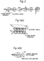
- liquid crystal compound which exhibits the SmC * phase is 2-methyl butyl P-[(P-n-decyloxy benzylidene) amino]. As shown in Figure 3 this liquid crystal compound is orientated in one direction, and has a spiral structure, i.e. the direction of orientation is twisted in each molecular layer.
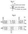
- the liquid crystal compound has two domains, one of which is inclined + ⁇ ° in the clockwise direction from the normal to the layers, and the other of which is inclined - ⁇ ° in the anticlockwise direction from the normal to the layers. These domains exist together as shown in Figure 5.
- a liquid crystal compound exhibiting the SmC * phase has an electric dipole perpendicular to the molecular axis, and when one domain has the electric dipole directed upwardly, the other domain has the electric dipole directed downwardly. Therefore, when an electric field is applied between the plates B, the liquid crystal molecules orientate either in a position +8° or -8° inclined to the normal to the layers. When the applied electric field is reversed the molecular orientation is reversed and the molecules orientate at a position either - ⁇ ° or +6° to the normal to the layers. Needless to say because the liquid crystal molecules have a polarising characteristic, when the liquid crystal cell is disposed between polarisers, optical bright-dark conditions occur depending upon the orientation of the liquid crystal molecules. Such a liquid crystal cell can be used as a liquid crystal display panel or a shutter array.
- a liquid crystal panel utilising a liquid crystal compound exhibiting the SmC * phase has the advantage of a very high response speed of the order of microseconds and has a memory characteristic which is retained for long periods even when the electric field is no longer applied.
- chiral smectic liquid crystal compounds have these characteristics was announced by Clark and L agerwall ( A ppl. P hys. Lett. 36, 899, 1980). These authors claim that chiral smectic liquid crystal compounds have another characteristic, namely a "desirable threshold value characteristic".
- the threshold value characteristic in this case, is not the threshold value characteristic towards the effective voltage as in a twisted nematic type liquid crystal compound, but is the characteristic only towards the value of applied voltage. Our experiments and those of other research institutions have failed to confirm the existence of a desirable threshold value characteristic.
- Figure 6 illustrated waveforms of signals used in this driving method.
- the electric potential applied to scanning electrodes is +Vap and -Vap at the selecting time
- a chiral smectic liquid crystal compound is driven by these signals whether the display is good or bad depends greatly on the orientation of the liquid crystal molecules.
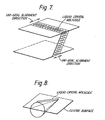
- the reason for this is that the molecular orientation achieved by uni-axial alignment treatment is stable but the condition where voltages applied and the molecules are aligned parallel to the plates of the liquid crystal cell causes large diformation.
- Figure 7 shows the molecular orientation when the surface of two plates is subject to a uni-axial alignment treatment.
- the layers are thought to be inclined to the thicker part of the plate and, when referring to one molecule, assuming an imaginary cone as in Figure 3, it is thought to be situated at the top surface of the cone as shown in Figure 8.
- the molecules are thought to be parallel to the plate, and situated at the top surface of the imaginary cone.
- a ferro-electric liquid crystal electro-optical device comprising two opposed plates having electrodes on the inner surfaces thereof, and a ferro-electric liquid crystal material sandwiched between said plates characterised by one of said plates having an uni-axial alignment characteristic on the surface thereof in contact with the liquid crystal material and the other plate having a random homogeneous alignment characteristic on a surface thereof in contact with the liquid crystal material.
- said uni-axial alignment characteristic is obtained by rubbing a thin layer of polyimide, polyvinyl alcohol, a fluorin- containing polymer, silane or silicon dioxide provided on the said surface of said one plate.
- Said random homogeneous alignment characteristic may be obtained by a homeotropic alignment treatment to said surface of said other plate and thereafter a heat treatment.
- Said random homogeneous alignment characteristic may be biassed in the direction of the uni-axial alignment characteristic.
- the angle between the direction of the bias and the direction of the uni-axial alignment treatment on said one plate is substantially equal to the tilt angle of the liquid crystal material.
- said random homogeneous alignment characteristic is biassed in the direction of the uni-axial alignment treatment by rubbing said surface of said other plate prior to said heat treatment.
- said random homogeneous alignment characteristic is biassed in the direction of the uni-axial alignment treatment by rubbing said surface of said other plate after said heat treatment.
- said random homogeneous alignment characteristic is biassed in the direction of the uni-axial alignment treatment by rubbing said surface of said other plate prior to said homeotropic alignment treatment.
- said random homogeneous alignment characteristic is obtained by providing a layer of polyimide, epoxy, polyvinyl alcohol, fluorine-containing polymer, polyurethane, silane, phenol,urea, silicon dioxide or magnesium fluoride on said surface of said other plate, without rubbing.
- said random honogemeous alignment characteristic is obtained by providing no alignment layer on said surface of said other plate.
- the liquid crystal material may be a chiral smectic liquid crystal material.
- the ferro-electric liquid crystal electro-optical device may be a display device or a shutter for a camera.
- a smectic liquid crystal electro-optical device comprising two, parallel plates with a ferro-electric chiral smectic liquid crystal material in a gap therebetween, said gap being less than the spiral pitch of the liquid crystal material characterised in that one of the plates has an uni-axial alignment characteristic on a surface thereof in contact with the liquid crystal material and the other plate has either a random homogeneous alignment characteristic or no alignment characteristic on the surface thereof in contact with the liquid crystal material.
- a ferro-electric liquid crystal electro-optical device comprising two electrode-holding plates at least one of which is transparent and between which is sandwiched a ferro-electric liquid crystal material, and means for selecting on-off conditions by a selecting voltage 4-Vap and for memorising the on-off conditions with an AC pulse whose width is smaller than that of the said voltage Vap and which has equal positive and negative amplitude characterised in that one plate has a uni-axial alignment treatment characteristic on th surface thereof in contact with the liquid cyrstal material and the other plate has a random homogeneous alignment treatment or no alignment treatment on the surface thereof in contact with the liquid crystal material.
- Random homogeneous alignment treatment means treatment which aligns the liquid crystal molecules close to parallel to the plates but does not let the molecules have any definite directional characteristic, but, this treatment includes alignment that lets the molecules have a weak uni-axial alignment characteristic by a weak rubbing treatment, etc.
- the random homogeneous alignment region serves to form an interface between the domain of the uni-axial alignment region and the domain grown under the effect of the uni-axial alignment region, into a free interface.
- "Free” in this case means that the mutual effect between the upper and lower molecules having the interface as a border, is very small. Therefore, the liquid crystal molecules 3 grown from the uni-axial alignment film 1b can exist in the most stable position without being forced. That position is horizontal to a plate 1, and is situated on the crossing line of the imaginary cone and the centre surface. This position is the ⁇ position already discussed.
- a polyimide thin film was formed by printing or dipping, and then rubbed in one direction to form a uni-axial alignment film.
- a silicon dioxide sputtered plate was immersed in 0.01 to 5.0 weight % organic silane homeotropic alignment compound water solution, washed and dried, then heat treatment was conducted for about 30 minutes at about 300°C to form a random homogeneous alignment film.
- the suitability of the driving method described above depends greatly on the temperature of the heat treatment. A temperature of 250 0 C to 300°C is, therefore, preferred.
- organic silane homeotropic alignment compounds the following are suitable:
- the uni-axial alignment treatment was the same as in Example 1.
- an organic silane compound was utilised.
- the alignment treatment with the organic silane compound was as follows: a silicon dioxide sputtered plate was immersed in 0.01 to 5.0 weight % of organic silane compound water solution, washed and dried.
- organic silane compound the following compounds are suitable:
- one plate 1 of the ferro-electric liquid crystal electro-optical device according to the present invention consisted of a polyimide thin film formed on a surface of a transparent electrically insulated plate la of, for example, glass, by printing or dipping.
- the polyimide thin film was rubbed in one direction to form the uni-axial alignment film lb.
- the plate 2 opposite the plate 1 and parallel thereto consisted of an electrically insulating transparent plate 2a on which the random homogeneous alignment film 2b was provided.
- This film was provided by rubbing treatment in a direction B (Fig. 2) at an angle ⁇ to the direction A of rubbing of the plate 1.
- the angle ⁇ corresponds to the tilt angle of the molecules of the liquid crystal compound 3 which is to be enclosed between the plates 1,2.
- the explanation of the method to form the random homogeneous alignment film 2b is as follows. First, a film of silicon dioxide (Si0 2 ) was formed on the plate 2a by means of, for example, vaccum evaporation. Then uni-axial rubbing treatment was conducted at an angle ⁇ to the direction of rubbing of the uni-axial alignment film 1b on the plate 1. Next, this plate was immersed into a water solution of organic silane homeotropic alignment compound, washed and dried, and the silane homeotropic alignment treatment was conducted on it, then, a heat treatment process was performed for about 1 hour at 300°C. A random homogeneous alignment film 1b biassed in a uni-axial direction was formed.
- Si0 2 silicon dioxide
- Example 1 As the above organic silane homeotropic alignment compound, the compounds described in relation to Example 1 can be utilised.
- Example 3 As a modification of Example 3, after application of the silane homeotropic compound on the silicon dioxide film, the uni-axial rubbing was conducted in a direction at an angle ⁇ to the alignment direction of the uni-axial alignment layer 1b on the plate 1. Heat treatment was then conducted for about 1 hour at 300 C and the random homogeneous alignment film which was biassed in a uni-axial direction was formed.
- the silane homeotropic alignment compound was formed on the silicon dioxide film, heat treatment was conducted for about 1 hour at 300° C , and then uni-axial rubbing treatment was conducted in a direction at an angle to the alignment direction of the uni-axial alignment film. Thereupon, a random homogeneous alignment film which was biassed in the uni-axial direction was formed.
- the plates 1,2 have respective alignment treated surfaces with a predetermined gap, and a ferro-electric smectic liquid crystal material 3 which consisted of S-4-0 (2-methyl)butyl-resol ciliden-4-alkyl n-tyctyl aniline and P-n-octyl phenyl P' 6-methyl octyl oxybenzoate in admixture in equal proportions, was enclosed between the plates.
- Polarisers 4,5 were disposed on the surface of the plates i.,2 respectively to form a liquid crystal panel.
- the liquid crystal panel as stated in Examples 1 to 5, not only offered a background with a uniform display, but also have a very fast response characteristic at around 300 ⁇ sec, when an electric field was applied.
- a transparent electrode was formed on the electrically insulated transparent plate 2a, and a polyimide thin film was formed by printing, dipping and baking without rubbing was formed on this transparent plate to produce a random homogeneous alignment film 2b.
- This random homogeneous alignment film lets adjacent liquid crystal molecules orientate parallel to the plates, but does not let the molecules have any directional characteristic.
- the plate 1 has a transparent electrode 4 on the electrically insulating transparent plate la, and on the surface of the plate la, a polyimide thin film was mounted, and a uni-axial alignment film 1b was formed after the surface of this thin film had been rubbed in one direction only.
- These two plates 1,2 were disposed with a gap therebetween less than the spiral pitch of the liquid crystal compound with the random homogeneous alignment film 2b and the uni-axial alignment film 1b being parallel and facing each other.
- the uni-axial alignment film and the random homogeneous alignment film were both formed by a polyimide film on the surface of the plates but materials other than polyimide can be used such as polyvinyl alcohol, a fluoro resin, e.g. a fluorine-containing polymer, silane or an oblique vacuum evaporated silicon dioxide film can be used for the uni-axial alignment film.
- materials other than polyimide such as polyvinyl alcohol, a fluoro resin, e.g. a fluorine-containing polymer, silane or an oblique vacuum evaporated silicon dioxide film can be used for the uni-axial alignment film.
- organic films such as epoxy, polyvinyl alcohol, fluoro resin.e.g. fluorine-containing polymer, polyurethane, silane, phenyl, urea, and inorganic films which are vacuum evaporated such as silicon dioxide or magnesium fluoride can be utilised.
- the random homogeneous alignment treatment of the plate 2 or the film 2b is not essential and the plate 2b can have no orientation process performed on it.
- the smectic liquid crystal material can hold the bi-stable condition and have a good memorising characteristic, and by initially orientating liquid crystal molecules in a direction which responds to the uni-axial alignment direction, it is possible to achieve a liquid crystal panel having a uniform background.
Landscapes
- Physics & Mathematics (AREA)
- Nonlinear Science (AREA)
- Chemical & Material Sciences (AREA)
- Crystallography & Structural Chemistry (AREA)
- General Physics & Mathematics (AREA)
- Optics & Photonics (AREA)
- Spectroscopy & Molecular Physics (AREA)
- Mathematical Physics (AREA)
- Liquid Crystal (AREA)
Applications Claiming Priority (6)
| Application Number | Priority Date | Filing Date | Title |
|---|---|---|---|
| JP142944/84 | 1984-07-10 | ||
| JP14294484A JPS6120930A (ja) | 1984-07-10 | 1984-07-10 | 強誘電性液晶電気光学装置 |
| JP215366/84 | 1984-10-15 | ||
| JP21536684A JPS6194029A (ja) | 1984-10-15 | 1984-10-15 | スメクテイツク液晶表示パネル及びその製造方法 |
| JP7778385A JPS61236523A (ja) | 1985-04-12 | 1985-04-12 | スメクテイツク液晶表示パネル |
| JP77783/85 | 1985-04-12 |
Publications (3)
| Publication Number | Publication Date |
|---|---|
| EP0168242A2 true EP0168242A2 (de) | 1986-01-15 |
| EP0168242A3 EP0168242A3 (en) | 1988-01-27 |
| EP0168242B1 EP0168242B1 (de) | 1991-10-09 |
Family
ID=27302518
Family Applications (1)
| Application Number | Title | Priority Date | Filing Date |
|---|---|---|---|
| EP85304896A Expired - Lifetime EP0168242B1 (de) | 1984-07-10 | 1985-07-09 | Elektrooptische Vorrichtung mit einem ferroelektrischen Flüssigkristall |
Country Status (3)
| Country | Link |
|---|---|
| US (1) | US4662721A (de) |
| EP (1) | EP0168242B1 (de) |
| DE (1) | DE3584326D1 (de) |
Cited By (6)
| Publication number | Priority date | Publication date | Assignee | Title |
|---|---|---|---|---|
| WO1986006506A1 (en) * | 1985-04-26 | 1986-11-06 | American Telephone & Telegraph Company | Alignment technique for liquid crystal devices |
| EP0219965A1 (de) * | 1985-09-18 | 1987-04-29 | Seiko Instruments Inc. | Elektrooptische Vorrichtung mit einem ferroelektrischen Flüssigkristall |
| GB2187026A (en) * | 1986-02-24 | 1987-08-26 | Rca Corp | Display device |
| EP0286539A1 (de) * | 1987-04-10 | 1988-10-12 | Commissariat A L'energie Atomique | Bistabile smektische ferroelektrische Flüssigkristall-Anzeigevorrichtung |
| EP0386782A2 (de) * | 1989-03-09 | 1990-09-12 | Matsushita Electric Industrial Co., Ltd. | Orientierungsfilm für Flüssigkristall und sein Herstellungsverfahren und Flüssigkristall-Anzeige unter Verwendung eines solchen Orientierungsfilms und Verfahren zu deren Herstellung |
| EP0695965A3 (de) * | 1994-08-04 | 1997-01-15 | Canon Kk | Flüssigkristallvorrichtung |
Families Citing this family (21)
| Publication number | Priority date | Publication date | Assignee | Title |
|---|---|---|---|---|
| JPS62112128A (ja) * | 1985-11-11 | 1987-05-23 | Semiconductor Energy Lab Co Ltd | 液晶装置 |
| US4820026A (en) * | 1986-03-20 | 1989-04-11 | Canon Kabushiki Kaisha | Ferroelectric liquid crystal device with modified polyvinyl alcohol alignment film |
| GB8616165D0 (en) * | 1986-07-02 | 1986-08-06 | Stc Plc | Liquid crystal cell |
| JP2530432B2 (ja) * | 1986-07-22 | 1996-09-04 | キヤノン株式会社 | 液晶素子 |
| US5061044A (en) * | 1989-05-23 | 1991-10-29 | Citizen Watch Co., Ltd. | Ferroelectric liquid crystal display having opposingly inclined alignment films wherein the liquid crystal has one twisted and two aligned states which coexist and a driving method to produce gray scale |
| JP2551848B2 (ja) * | 1989-07-25 | 1996-11-06 | セイコープレシジョン株式会社 | 強誘電性液晶パネル |
| US5646704A (en) * | 1989-10-26 | 1997-07-08 | Canon Kabushiki Kaisha | Chiral smectic liquid crystal device having predetermined pre-tilt angle and intersection angle |
| US5200238A (en) * | 1990-06-22 | 1993-04-06 | Loctite (Ireland) Limited | Liquid crystal display devices and method of manufacture |
| CA2051191C (en) * | 1990-09-13 | 1996-07-09 | Shuzo Kaneko | Optical modulation element |
| JPH04142514A (ja) * | 1990-10-03 | 1992-05-15 | Semiconductor Energy Lab Co Ltd | 強誘電性液晶装置 |
| JP3013260B2 (ja) * | 1990-11-19 | 2000-02-28 | 株式会社半導体エネルギー研究所 | 液晶装置 |
| US5490001A (en) * | 1990-11-19 | 1996-02-06 | Semiconductor Energy Laboratory Co., Ltd. | Ferroelectric liquid crystal device with an AC electric field producing a helical structure |
| US5172257A (en) * | 1991-11-08 | 1992-12-15 | Bell Communications Research, Inc. | Twisted ferroelectric liquid crystal modulator for providing gray scale |
| US5739882A (en) * | 1991-11-18 | 1998-04-14 | Semiconductor Energy Laboratory Co., Ltd. | LCD polymerized column spacer formed on a modified substrate, from an acrylic resin, on a surface having hydrophilic and hydrophobic portions, or at regular spacings |
| US5559620A (en) * | 1992-03-05 | 1996-09-24 | Casio Computer Co., Ltd. | Anti-ferroelectric liquid crystal display device with intersecting alignment film directions |
| EP0797787A1 (de) * | 1995-10-16 | 1997-10-01 | Koninklijke Philips Electronics N.V. | Optische modulationsvorrichtung und solch eine modulationsvorrichtung enthaltende dhflc-anzeige |
| US5943108A (en) * | 1996-07-12 | 1999-08-24 | Canon Kabushiki Kaisha | Matrix type liquid crystal display with substrate having blue filter for masking at least 75% of total planar area of auxiliary electrodes |
| US5790221A (en) * | 1996-08-30 | 1998-08-04 | Industrial Technology Research Institute | Method of manufacturing a liquid crystal cell |
| US20040196428A1 (en) | 2003-01-16 | 2004-10-07 | Nano Loa, Inc. | Liquid crystal display device |
| KR20140115180A (ko) * | 2013-03-20 | 2014-09-30 | 삼성디스플레이 주식회사 | 액정 표시 장치 및 그 제조 방법 |
| CN114063337B (zh) * | 2020-08-07 | 2024-01-26 | 马耀东 | 外延取向液晶显示器 |
Citations (4)
| Publication number | Priority date | Publication date | Assignee | Title |
|---|---|---|---|---|
| US3991241A (en) * | 1974-06-13 | 1976-11-09 | Tokyo Shibaura Electric Co., Ltd. | Liquid crystal device |
| EP0091661A1 (de) * | 1982-04-07 | 1983-10-19 | Hitachi, Ltd. | Optisches Modulationselement mit Flüssigkristallen |
| EP0091637A2 (de) * | 1982-04-05 | 1983-10-19 | Hitachi, Ltd. | Flüssigkristallanzeigevorrichtung |
| DE3427597A1 (de) * | 1983-07-29 | 1985-02-07 | American Telephone And Telegraph Co., New York, N.Y. | Ausrichtung von ferroelektrischen fluessigkristall-anzeigevorrichtungen |
Family Cites Families (7)
| Publication number | Priority date | Publication date | Assignee | Title |
|---|---|---|---|---|
| US3930716A (en) * | 1972-03-31 | 1976-01-06 | Commissariat A L'energie Atomique | Method of collecting orientation of the molecules of a liquid crystal and a liquid-crystal cell for carrying out said method |
| JPS536857B2 (de) * | 1972-08-16 | 1978-03-11 | ||
| US4030997A (en) * | 1975-04-21 | 1977-06-21 | Hughes Aircraft Company | Method of aligning liquid crystals |
| GB1543599A (en) * | 1976-05-04 | 1979-04-04 | Standard Telephones Cables Ltd | Liquid crystal cell |
| JPS53116169A (en) * | 1977-03-18 | 1978-10-11 | Citizen Watch Co Ltd | Reflection type liquid crystal color display device |
| DE2827471C2 (de) * | 1978-06-22 | 1982-09-02 | Siemens AG, 1000 Berlin und 8000 München | Flüssigkristallzelle mit einer induzierten cholesterischen Phase |
| JP3701078B2 (ja) * | 1996-06-18 | 2005-09-28 | タカラ技研株式会社 | 道路床版工法 |
-
1985
- 1985-06-28 US US06/750,092 patent/US4662721A/en not_active Expired - Lifetime
- 1985-07-09 EP EP85304896A patent/EP0168242B1/de not_active Expired - Lifetime
- 1985-07-09 DE DE8585304896T patent/DE3584326D1/de not_active Expired - Lifetime
Patent Citations (4)
| Publication number | Priority date | Publication date | Assignee | Title |
|---|---|---|---|---|
| US3991241A (en) * | 1974-06-13 | 1976-11-09 | Tokyo Shibaura Electric Co., Ltd. | Liquid crystal device |
| EP0091637A2 (de) * | 1982-04-05 | 1983-10-19 | Hitachi, Ltd. | Flüssigkristallanzeigevorrichtung |
| EP0091661A1 (de) * | 1982-04-07 | 1983-10-19 | Hitachi, Ltd. | Optisches Modulationselement mit Flüssigkristallen |
| DE3427597A1 (de) * | 1983-07-29 | 1985-02-07 | American Telephone And Telegraph Co., New York, N.Y. | Ausrichtung von ferroelektrischen fluessigkristall-anzeigevorrichtungen |
Non-Patent Citations (1)
| Title |
|---|
| FERROELECTRICS, vol. 59, 1984, New York J.S. PATEL et al. "A reliable method of alignment for smedic liquid crystals" pages 137-144 * |
Cited By (16)
| Publication number | Priority date | Publication date | Assignee | Title |
|---|---|---|---|---|
| WO1986006506A1 (en) * | 1985-04-26 | 1986-11-06 | American Telephone & Telegraph Company | Alignment technique for liquid crystal devices |
| US4792211A (en) * | 1985-09-18 | 1988-12-20 | Seiko Instruments & Electronics Ltd. | Ferroelectric liquid crystal electro-optical device having high water repellent alignment layer |
| EP0219965A1 (de) * | 1985-09-18 | 1987-04-29 | Seiko Instruments Inc. | Elektrooptische Vorrichtung mit einem ferroelektrischen Flüssigkristall |
| GB2187026A (en) * | 1986-02-24 | 1987-08-26 | Rca Corp | Display device |
| FR2594992A1 (fr) * | 1986-02-24 | 1987-08-28 | Rca Corp | Dispositif d'affichage a cristal liquide |
| GB2187026B (en) * | 1986-02-24 | 1989-11-08 | Rca Corp | Display device |
| US4902106A (en) * | 1987-04-10 | 1990-02-20 | Commissariat A L'energie Atomique | Bistable ferroelectric smectic liquid crystal display device having particular orientation film |
| FR2613846A1 (fr) * | 1987-04-10 | 1988-10-14 | Commissariat Energie Atomique | Dispositif d'affichage a cristal liquide smectique ferroelectrique bistable |
| EP0286539A1 (de) * | 1987-04-10 | 1988-10-12 | Commissariat A L'energie Atomique | Bistabile smektische ferroelektrische Flüssigkristall-Anzeigevorrichtung |
| EP0386782A2 (de) * | 1989-03-09 | 1990-09-12 | Matsushita Electric Industrial Co., Ltd. | Orientierungsfilm für Flüssigkristall und sein Herstellungsverfahren und Flüssigkristall-Anzeige unter Verwendung eines solchen Orientierungsfilms und Verfahren zu deren Herstellung |
| EP0386782A3 (de) * | 1989-03-09 | 1991-08-07 | Matsushita Electric Industrial Co., Ltd. | Orientierungsfilm für Flüssigkristall und sein Herstellungsverfahren und Flüssigkristall-Anzeige unter Verwendung eines solchen Orientierungsfilms und Verfahren zu deren Herstellung |
| US5133895A (en) * | 1989-03-09 | 1992-07-28 | Matsushita Electric Industrial Co., Ltd. | Alignment film for liquid crystal and method for production thereof, as well as liquid crystal display device utilizing said alignment film and method for production thereof |
| EP0635747A1 (de) * | 1989-03-09 | 1995-01-25 | Matsushita Electric Industrial Co., Ltd. | Orientierungsfilm für Flussigkristall und sein Herstellungsverfahren |
| US5515190A (en) * | 1989-03-09 | 1996-05-07 | Matsushita Electric Industrial Co., Ltd. | Alignment film with long and short carbon chains absorbed silane with liquid crystal attached |
| EP0695965A3 (de) * | 1994-08-04 | 1997-01-15 | Canon Kk | Flüssigkristallvorrichtung |
| US5831705A (en) * | 1994-08-04 | 1998-11-03 | Canon Kabushiki Kaisha | Liquid crystal device |
Also Published As
| Publication number | Publication date |
|---|---|
| EP0168242B1 (de) | 1991-10-09 |
| EP0168242A3 (en) | 1988-01-27 |
| US4662721A (en) | 1987-05-05 |
| DE3584326D1 (de) | 1991-11-14 |
Similar Documents
| Publication | Publication Date | Title |
|---|---|---|
| EP0168242A2 (de) | Elektrooptische Vorrichtung mit einem ferroelektrischen Flüssigkristall | |
| Barberi et al. | Electrochirally controlled bistable surface switching in nematic liquid crystals | |
| JPH0812360B2 (ja) | 液晶表示装置およびその駆動方法 | |
| US5514426A (en) | Liquid crystal device | |
| JPH04251218A (ja) | 強誘電性液晶装置 | |
| JPH0812346B2 (ja) | 強誘電性液晶の配向方法 | |
| US5465169A (en) | Ferroelectric liquid crystal device with electroconductive protective film and electroconductive alignment film | |
| JP3136052B2 (ja) | 強誘電性液晶素子 | |
| EP0323231A1 (de) | Verschluss mit einem ferroelektrischen Flüssigkristall | |
| US4995706A (en) | Liquid crystal device with a ferroelectric thin film | |
| JPS6236634A (ja) | 液晶表示素子 | |
| US5973762A (en) | Ferroelectric liquid crystal cell with a monochevron structure of smectic layers | |
| JP2550054B2 (ja) | 強誘電性スメクチツク液晶電気光学装置 | |
| EP0200427B1 (de) | Elektrooptische Vorrichtung mit chiral smektischem Flüssigkristall und Verfahren zu deren Ansteuerung | |
| JPH0245170B2 (ja) | Sumekuteitsukuekishosochiniokeruekishobutsushitsuchunyuhoho | |
| JPH0733217Y2 (ja) | スメクテイツク型液晶表示素子 | |
| KR100477132B1 (ko) | 강유전성 액정 물질을 사용하는 액정 표시 장치의 제조 방법 | |
| JPH0711632B2 (ja) | カイラルスメクチック液晶素子の電圧印加方法 | |
| JPH0526174B2 (de) | ||
| JPH06103370B2 (ja) | 液晶表示装置 | |
| JPH0756545B2 (ja) | 液晶マトリツクス表示パネルの駆動法 | |
| JPH0588154A (ja) | 強誘電液晶素子 | |
| JPH0743722A (ja) | 液晶素子 | |
| JPH0695612A (ja) | 強誘電性液晶素子の電圧印加駆動方法 | |
| JP2609856B2 (ja) | 電気光学装置 |
Legal Events
| Date | Code | Title | Description |
|---|---|---|---|
| PUAI | Public reference made under article 153(3) epc to a published international application that has entered the european phase |
Free format text: ORIGINAL CODE: 0009012 |
|
| AK | Designated contracting states |
Designated state(s): DE FR GB |
|
| RAP1 | Party data changed (applicant data changed or rights of an application transferred) |
Owner name: SEIKO INSTRUMENTS INC. |
|
| PUAL | Search report despatched |
Free format text: ORIGINAL CODE: 0009013 |
|
| RHK1 | Main classification (correction) |
Ipc: G02F 1/137 |
|
| AK | Designated contracting states |
Kind code of ref document: A3 Designated state(s): DE FR GB |
|
| 17P | Request for examination filed |
Effective date: 19880630 |
|
| 17Q | First examination report despatched |
Effective date: 19900131 |
|
| GRAA | (expected) grant |
Free format text: ORIGINAL CODE: 0009210 |
|
| AK | Designated contracting states |
Kind code of ref document: B1 Designated state(s): DE FR GB |
|
| REF | Corresponds to: |
Ref document number: 3584326 Country of ref document: DE Date of ref document: 19911114 |
|
| ET | Fr: translation filed | ||
| PLBE | No opposition filed within time limit |
Free format text: ORIGINAL CODE: 0009261 |
|
| STAA | Information on the status of an ep patent application or granted ep patent |
Free format text: STATUS: NO OPPOSITION FILED WITHIN TIME LIMIT |
|
| 26N | No opposition filed | ||
| REG | Reference to a national code |
Ref country code: GB Ref legal event code: 746 Effective date: 19940607 |
|
| REG | Reference to a national code |
Ref country code: FR Ref legal event code: DL |
|
| REG | Reference to a national code |
Ref country code: GB Ref legal event code: IF02 |
|
| PGFP | Annual fee paid to national office [announced via postgrant information from national office to epo] |
Ref country code: GB Payment date: 20040707 Year of fee payment: 20 |
|
| PGFP | Annual fee paid to national office [announced via postgrant information from national office to epo] |
Ref country code: FR Payment date: 20040708 Year of fee payment: 20 |
|
| PGFP | Annual fee paid to national office [announced via postgrant information from national office to epo] |
Ref country code: DE Payment date: 20040722 Year of fee payment: 20 |
|
| PG25 | Lapsed in a contracting state [announced via postgrant information from national office to epo] |
Ref country code: GB Free format text: LAPSE BECAUSE OF EXPIRATION OF PROTECTION Effective date: 20050708 |
|
| REG | Reference to a national code |
Ref country code: GB Ref legal event code: PE20 |