EP0200402B1 - Abtast- und Haltestromkreis - Google Patents
Abtast- und Haltestromkreis Download PDFInfo
- Publication number
- EP0200402B1 EP0200402B1 EP86302684A EP86302684A EP0200402B1 EP 0200402 B1 EP0200402 B1 EP 0200402B1 EP 86302684 A EP86302684 A EP 86302684A EP 86302684 A EP86302684 A EP 86302684A EP 0200402 B1 EP0200402 B1 EP 0200402B1
- Authority
- EP
- European Patent Office
- Prior art keywords
- output
- switching element
- input
- sample
- hold
- Prior art date
- Legal status (The legal status is an assumption and is not a legal conclusion. Google has not performed a legal analysis and makes no representation as to the accuracy of the status listed.)
- Expired
Links
Images

Classifications
-
- G—PHYSICS
- G11—INFORMATION STORAGE
- G11C—STATIC STORES
- G11C27/00—Electric analogue stores, e.g. for storing instantaneous values
- G11C27/02—Sample-and-hold arrangements
- G11C27/024—Sample-and-hold arrangements using a capacitive memory element
- G11C27/026—Sample-and-hold arrangements using a capacitive memory element associated with an amplifier
Definitions
- This invention relates to a sample and hold circuit which may be used as a liquid crystal panel driving circuit or the like of a television receiver.
- Liquid crystal television receivers employing liquid crystal panels as display elements have been developed recently. To begin with, the outline of operation of such a liquid crystal television receiver is described below.
- Fig. 4 shows a general construction of a liquid crystal television receiver.
- Television signals sent from a broadcasting station are received by an antenna 1, and are converted in frequency by a tuner 2 to an intermediate frequency.
- the intermediate frequency signals are amplified and detected in signal processing circuit 3, and audio signals and video signals are obtained.
- the audio signals are delivered to a speaker 5 by way of an audio output circuit 4, while video signals are applied to a chroma stage 6 and a control unit 7.
- the chroma stage 6 comprises a chroma processing unit and chroma output unit, and the video signals are demodulated into R, G, B signals in the chroma processing unit, and are converted into signals inverted in the polarity in every field by the chroma output unit to be applied to a Y driver IC 9.
- the video signals applied to the Y driver IC 9 are sample-held, and are applied to the source line of an active matrix liquid crystal panel 8.
- the video signals fed to the control unit 7, in which various control pulses are obtained are applied to the control signal input terminals of X driver IC 10 and Y driver IC 9.
- the X driver IC 10 is intended to scan in the vertical direction, and its output is applied to the gate line of active matrix liquid crystal panel 8. Thus, by the vertical direction scanning pulses from the X driver IC 10 and video signals from the Y driver IC 9, a television picture is obtained on the active matrix liquid crystal panel 8.
- Y driver IC 9 an example of composition of Y driver IC is shown in Fig. 5.
- the R, G, B signals from the chroma stage are applied to R, G, B terminals, and are changed over in every horizontal period by an analog multiplexer 11 to be led into three video signal lines 12.
- the analog multiplexer 11 changes over according to the R, G, B picture element arrangement on the liquid crystal panel.
- Numeral 13 denotes a shift register, which receives clock ⁇ Y and start pulse S, and delivers sampling pulses Q1, Q2 and so forth sequentially.
- Numeral 14 denotes a sample and hold circuit and operational amplifier, which are designed to sample the video signals from the video signal line 12 according to the sample pulses Q1, Q2 and so forth from the shift register, and hold them according to the pulses G1, G2 applied from outside.
- the outputs of the sample and hold circuit and operational amplifier 14 are connected to output terminals Y01, Y02, Vietnamese output terminals are connected to the source line of the active matrix liquid crystal panel.
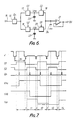
- Fig. 6 The sample and hold circuit and one (the n-th) of the operational amplifiers in Fig. 5 are shown in Fig. 6, in which numeral 15 denotes a video signal line, and 16 to 20 are switching circuits which operate to turn on when the pulse of the signal indicated by each arrow is high level, and turn off when it is low level.
- numeral 16 is a switching circuit for video signal sampling, and its output is applied to two input switching circuits 17, 18, and hold capacitors 22, 23 are connected to output switching circuits 19, 20 are connected to the output terminals of input switching circuit, while output terminals of hold capacitors.
- Output terminals of these two output switching circuits are mutually coupled together, and are connected to the input terminal of operational amplifier 21 having an input capacitance 24, and the output of operational amplifier becomes output Y 0n of Y driver IC, and is connected to the source line of liquid crystal panel.
- Waveforms of the sample and hold circuit and individual parts of operational amplifiers in Fig. 6 are shown in Fig. 7, in which V is a video signal applied to the video signal line 15, and one horizontal period is represented by H.
- G1, G2 are control pulses applied to switching circuits 17 to 20 of sample hold, and the period of both G1 and G2 is 2H, and their phases are mutually deviated by ⁇ .
- ⁇ In order to perform the sample hold securely, there is a period t in which both G1 and G2 are off.
- the period in which either G1 or G2 is on is indicated by t1, t2, Across Q n is an n-th output pulse of shift register 13, and it is a video signal sampling pulse to open or close the switching circuit 16.
- V na and V nb are voltage waveforms applied to hold capacitors 22, 23 and Y 0n is an n-th output waveform of Y driver IC.
- G2 is on and G1 is off, so that the information V na of hold capacitor 22 is transmitted to the output Y 0n of Y driver IC, and video information V nb is sampled in the hold capacitor 23 by the sampling pulse of Q n .
- the input capacitance 24 is always present at the input side of operational amplifier 21, and when the operational amplifier is composed of CMOS, in particular, the value of input capacitance is considerably large.
- the value of input capacitance 24 of operational amplifier is generally too great to be ignored, and, therefore, when the output side switching circuits 19, 20 are turned on, the voltage being held by the hold capacitors 22, 23 is influenced by the electric charge 1H before as being accumulated in the input capacitance 24 of the operational amplifier 21 in the output Y 0n of Y driver IC, so that the input voltage may not be delivered at high fidelity.
- this invention is intended to present a sample and hold circuit which is capable of eliminating the adverse effects of the capacitance component if a capacitance component is present at the output side.
- US patent no. 4366456 (Ueno et al) describes a signal convertor adapted to output so-called 100% sample and hold signals, VS100, to a switched capacitor filter.
- This signal converter may comprise an input switching element having an input terminal for receiving the input signal VS" in , a hold capacitor connected between an output terminal of said input switching element and a reference potential, and an output switching element connected to the output terminal of the input switching element (see Fig. 8 and Fig. 10).
- the signal converter of the Ueno et al patent is adapted to eliminate the gaps (non-holding terms) which occur in the input signal thereof by the provision of additional sets of input switching element-hold capacitor-output switching element assemblies, connected in parallel with the first, and adapted so that the hold capacitors thereof successively discharge to the output during the gaps in the input signal.
- the present invention provides a sample and hold circuit comprising: an input switching element for sampling an input signal; a hold capacitor connected between an output terminal of the input switching element and a reference potential; and an output switching element connected to an output terminal of said input switching element; said input switching element and said output switching element being adapted to conduct alternatively, characterized in that: a discharge switching element is connected between the output terminal of said output switching element and said reference potential; and said discharge switching element is adapted to conduct for a short period immediately before said output switching element conducts whereby to discharge the capacitance of an output element connected, in use, to the output terminal of the output switching element so as to return its output potential to said reference potential.
- This invention having the above construction, can discharge the electric charge of the capacity component accumulated so far, by means of the switching element for discharge, immediately before the output from the hold capacity is applied to the capacity component of the output side, and can return the output potential to the reference potential so that the next hold voltage may be accurately delivered regardless of the previous output signal value.
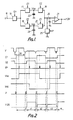
- Fig. 1 shows the construction of a sample and hold circuit in the embodiment of this invention, in which numerals 15 to 24 corresponds to the parts of the conventional construction shown in Fig. 6.
- a switching circuit 25 which is turned on and off by P pulse is installed between the output side of the sample and hold circuit and reference potential.
- Fig. 2 shows the waveforms of various parts of the sample hold circuit in Fig. 1, in which a P pulse which is applied immediately before G1 or G2 is turned on so as to discharge the electric charge accumulated in the capacity component 24. That is, since the output Y 0n of the Y driver IC is returned to the reference potential when the P pulse is turned on, the voltage is always proportional to the sampled video signal regardless of the effect of the hold voltage 1H before. Therefore, as shown in Fig. 7 there is no step difference in the Y 0n value between t2 period and t3 period, and the voltage of same level is obtained.
- a sample and hold circuit capable of delivering outputs always correctly corresponding to the input video signals without being influenced by the video signal level 1H before may be realized.
- each switching element is composed of parallel circuits of p-channel MOS and n-channel MOS.
- Q n , G 1, G 2, P represent the polarity inverted pulses of Q n , G1, G2, P respectively.
- the operational amplifier 21 is composed of aluminium bate CMOS, its input capacity 24 is about 0.4 to 1pF.
- the value of hold capacitors 22, 23 are several pF, effects of video signal level 1H before may be present about 10 to 20% if there is no switching element 25.
- a sample and hold circuit capable of delivering outputs always correctly corresponding to the input video signal without being influenced by the video signal level 1H before may be realized.
Landscapes
- Liquid Crystal Display Device Control (AREA)
- Transforming Electric Information Into Light Information (AREA)
Claims (7)
- Abtast-Halte-Schaltkreis mit:
einem Eingangsschaltelement (17) zum Abtasten eines Eingangssignals;
einem Haltekondensator (22), der zwischen einem Ausgangsanschluß des Eingangsschaltelements (17) und einem Bezugspotential angeschlossen ist; und
einem Ausgangsschaltelement (19), das mit einem Ausgangsanschluß des Eingangsschaltelements verbunden ist;
wobei das Eingangsschaltelement (17) und das Ausgangsschaltelement (19) geeignet sind, abwechselnd zu leiten, dadurch gekennzeichnet, daß ein Entladungschaltelement (25) zwischen dem Ausgangsanschluß des Ausgangsschaltelements und dem Bezugspotential angeschlossen ist und daß das Entladungsschaltelement (25) geeignet ist, für eine kurze Periode, unmittelbar bevor das Ausgangsschaltelement (19) leitet, zu leiten, wodurch die Kapazität eines Ausgangselements, das im Betrieb mit dem Ausgangsanschluß des Ausgangsschaltelements (19) verbunden ist, entladen wird, so daß sein Ausgangspotential auf das Bezugspotential zurückgefuhrt wird. - Abtast-Halte-Schaltkreis nach Anspruch 1, bei dem Paare dieser Eingangsschaltelemente (17, 18) und Ausgangsschaltelemente (19, 20) und der Haltekondensatoren (22, 23) vorgesehen sind und bei dem die Paare von Eingangsschaltelementen (17, 18) und Ausgangsschaltelementen (19, 20) abwechselnd geschaltet werden.
- Abtast-Halte-Schaltkreis nach Anspruch 1 oder 2, bei dem das Eingangssignal ein Videosignal ist und die Eingangs(17, 18) und Ausgangs- (19, 20) Schaltelemente während einer horizontalen Periode des Videosignals geschaltet werden.
- Vorrichtung, welche umfaßt:
einen Abtast-Halte-Schaltkreis mit einem Eingangsschaltelement (17) zum Abtasten eines Eingangssignals, einem Haltekondensator (22), der zwischen einem Ausgangsanschluß des Eingangsschaltelements (17) und einem Bezugspotential angeschlossen ist, einem Ausgangsschaltelement (19), das mit einem Ausgangsanschluß des Eingangsschaltelements (17) verbunden ist, und einen Verstärkerschaltkreis (21) mit einer Eingangskapazität;
wobei der Verstärkerschaltkreis mit dem Ausgangsanschluß des Ausgangsschaltelements (19) des Abtast-Halte-Schaltkreises so verbunden ist, daß die Eingangskapazität des Verstärkerschaltkreises (21) an der Ausgangsseite des Ausgangsschaltelements (19) vorhanden ist;
wobei das Eingangsschaltelement (17) und das Ausgangsschaltelement (19) des Abtast-Halte-Schaltkreises geeignet sind, abwechselnd zu leiten, dadurch gekennzeichnet, daß ein Entladungschaltelement (25) zwischen einem Ausgangsanschluß des Ausgangsschaltelements und dem Bezugspotential angeschlossen ist und daß das Entladungsschaltelement (25) des Abtast-Halte-Schaltkreises geeignet ist, für eine kurze Periode, unmittelbar bevor das Ausgangsschaltelement (19) leitet, zu leiten, wodurch die Kapazität entladen wird, so daß sein Ausgangspotential auf das Bezugspotential zurückgeführt wird. - Vorrichtung nach Anspruch 4, wobei der Verstärkerschaltkreis ein MOS-Typ-Operationsverstärker ist.
- Vorrichtung nach Anspruch 5, bei der Paare dieser Eingangsschaltelemente (17, 18) und Ausgangsschaltelemente (19, 20) und der Haltekondensatoren (22, 23) vorgesehen sind und bei dem die Paare von Eingangsschaltelementen (17, 18) und Ausgangsschaltelementen (19, 20) abwechselnd geschaltet werden.
- Vorrichtung nach Anspruch 5, bei der das Eingangssignal ein Videosignal ist und die Eingangs- (17, 18) und Ausgangs- (19, 20) Schaltelemente während einer horizontalen Periode des Videosignals geschaltet werden.
Applications Claiming Priority (2)
| Application Number | Priority Date | Filing Date | Title |
|---|---|---|---|
| JP60075602A JPH0654961B2 (ja) | 1985-04-10 | 1985-04-10 | サンプルホ−ルド回路 |
| JP75602/85 | 1985-04-10 |
Publications (3)
| Publication Number | Publication Date |
|---|---|
| EP0200402A2 EP0200402A2 (de) | 1986-11-05 |
| EP0200402A3 EP0200402A3 (en) | 1988-07-06 |
| EP0200402B1 true EP0200402B1 (de) | 1991-08-14 |
Family
ID=13580915
Family Applications (1)
| Application Number | Title | Priority Date | Filing Date |
|---|---|---|---|
| EP86302684A Expired EP0200402B1 (de) | 1985-04-10 | 1986-04-10 | Abtast- und Haltestromkreis |
Country Status (4)
| Country | Link |
|---|---|
| US (1) | US4823027A (de) |
| EP (1) | EP0200402B1 (de) |
| JP (1) | JPH0654961B2 (de) |
| DE (1) | DE3680816D1 (de) |
Families Citing this family (28)
| Publication number | Priority date | Publication date | Assignee | Title |
|---|---|---|---|---|
| JPH0289438A (ja) * | 1988-09-27 | 1990-03-29 | Toshiba Corp | サンプリング回路 |
| JP2576606B2 (ja) * | 1988-10-13 | 1997-01-29 | 日本電気株式会社 | 出力ドライバ回路 |
| US4987321A (en) * | 1989-09-25 | 1991-01-22 | Eastman Kodak Company | Processing circuit for image sensor |
| US5162670A (en) * | 1990-01-26 | 1992-11-10 | Kabushiki Kaisha Toshiba | Sample-and-hold circuit device |
| US5111072A (en) * | 1990-08-29 | 1992-05-05 | Ncr Corporation | Sample-and-hold switch with low on resistance and reduced charge injection |
| FR2667188A1 (fr) * | 1990-09-21 | 1992-03-27 | Senn Patrice | Circuit echantillonneur-bloqueur pour ecran d'affichage a cristal liquide. |
| KR930004268B1 (ko) * | 1990-10-15 | 1993-05-22 | 금성일렉트론 주식회사 | 광대역 샘플/홀드회로 |
| JPH04179996A (ja) * | 1990-11-15 | 1992-06-26 | Toshiba Corp | サンプルホールド回路およびこれを用いた液晶ディスプレイ装置 |
| JP2833289B2 (ja) * | 1991-10-01 | 1998-12-09 | 日本電気株式会社 | アナログスイッチ |
| JP3067059B2 (ja) * | 1992-07-09 | 2000-07-17 | シャープ株式会社 | サンプルホールド回路 |
| JP2558586B2 (ja) * | 1993-01-11 | 1996-11-27 | キャスコ株式会社 | ゴルフボール |
| US5281867A (en) * | 1993-02-23 | 1994-01-25 | Motorola, Inc. | Multiple channel sampling circuit having minimized crosstalk interference |
| US5644257A (en) * | 1993-03-24 | 1997-07-01 | Crystal Semiconductor Corporation | Sampling circuit charge management |
| US5418533A (en) * | 1993-11-19 | 1995-05-23 | Tektronix, Inc. | Method and circuit for conditioning a signal for use in systems having analog-to-digital converter circuits |
| JP2747230B2 (ja) * | 1994-10-04 | 1998-05-06 | ローム株式会社 | 信号処理装置 |
| US6031398A (en) * | 1997-01-22 | 2000-02-29 | Lucent Technologies Inc. | Reduced-feedthrough switch circuit |
| EP0862270A1 (de) * | 1997-02-28 | 1998-09-02 | STMicroelectronics S.r.l. | Adaptiver Treppenspannungserzeugerstromkreis |
| US5963063A (en) * | 1997-08-26 | 1999-10-05 | Texas Instruments Incorporated | Sample and hold circuit having a waveform shaping circuit |
| DE19753279C2 (de) * | 1997-12-01 | 2001-03-08 | Sgs Thomson Microelectronics | Elektrische Schaltung mit mindestens einem geschalteten Kondensator und Verfahren zum Betreiben dieser Schaltung |
| US6943761B2 (en) * | 2001-05-09 | 2005-09-13 | Clare Micronix Integrated Systems, Inc. | System for providing pulse amplitude modulation for OLED display drivers |
| AU2002348472A1 (en) * | 2001-10-19 | 2003-04-28 | Clare Micronix Integrated Systems, Inc. | System and method for providing pulse amplitude modulation for oled display drivers |
| JP4046015B2 (ja) * | 2002-06-07 | 2008-02-13 | セイコーエプソン株式会社 | 電子回路、電子装置、電気光学装置及び電子機器 |
| US7170041B2 (en) * | 2002-07-17 | 2007-01-30 | Xerox Corporation | Pixel circuitry for imaging system |
| AU2003280128A1 (en) * | 2002-11-25 | 2004-06-18 | Koninklijke Philips Electronics N.V. | Sample and hold circuit |
| JP4536452B2 (ja) * | 2004-08-04 | 2010-09-01 | ルネサスエレクトロニクス株式会社 | 半導体集積回路および半導体集積回路への電源電圧供給方法 |
| US7683677B2 (en) * | 2007-08-06 | 2010-03-23 | Mediatek Inc. | Sample-and-hold amplification circuits |
| JP5102131B2 (ja) * | 2008-07-14 | 2012-12-19 | 株式会社豊田中央研究所 | ホールド回路 |
| JP6179718B2 (ja) * | 2013-10-01 | 2017-08-16 | セイコーNpc株式会社 | サンプルホールド回路 |
Family Cites Families (8)
| Publication number | Priority date | Publication date | Assignee | Title |
|---|---|---|---|---|
| US3226650A (en) * | 1964-03-09 | 1965-12-28 | Thomas E Higbie | Video pulse amplitude detector for airborne radar systems |
| JPS5842683B2 (ja) * | 1973-05-08 | 1983-09-21 | トヨタ精機工業 (株) | 鋼板製丸形電線接続箱製造方法 |
| FR2453471A1 (fr) * | 1979-04-06 | 1980-10-31 | Inst Francais Du Petrole | Echantillonneur-bloqueur perfectionne |
| JPS55166324A (en) * | 1979-06-14 | 1980-12-25 | Fujitsu Ltd | Switched capacitor filter |
| US4306196A (en) * | 1980-01-14 | 1981-12-15 | Bell Telephone Laboratories, Incorporated | Operational amplifier with offset compensation |
| JPS5884342A (ja) * | 1981-11-13 | 1983-05-20 | Toshiba Corp | 信号処理回路 |
| US4430622A (en) * | 1981-11-19 | 1984-02-07 | Gte Laboratories Incorporated | Offset correction circuit |
| JPS60214177A (ja) * | 1984-04-09 | 1985-10-26 | Sharp Corp | 液晶駆動回路 |
-
1985
- 1985-04-10 JP JP60075602A patent/JPH0654961B2/ja not_active Expired - Lifetime
-
1986
- 1986-04-10 EP EP86302684A patent/EP0200402B1/de not_active Expired
- 1986-04-10 DE DE8686302684T patent/DE3680816D1/de not_active Expired - Lifetime
-
1987
- 1987-10-19 US US07/111,093 patent/US4823027A/en not_active Expired - Lifetime
Also Published As
| Publication number | Publication date |
|---|---|
| US4823027A (en) | 1989-04-18 |
| EP0200402A3 (en) | 1988-07-06 |
| EP0200402A2 (de) | 1986-11-05 |
| DE3680816D1 (de) | 1991-09-19 |
| JPH0654961B2 (ja) | 1994-07-20 |
| JPS61234674A (ja) | 1986-10-18 |
Similar Documents
| Publication | Publication Date | Title |
|---|---|---|
| EP0200402B1 (de) | Abtast- und Haltestromkreis | |
| US5721563A (en) | Active matrix liquid crystal drive circuit capable of correcting offset voltage | |
| US4845382A (en) | Sampling and holding circuit for signal having low sampling residual component, especially for the dual sampling of a correlated signal given by a charge-transfer device | |
| JPH0654421B2 (ja) | マトリクス型液晶表示装置の列電極駆動回路 | |
| US4970594A (en) | Television video signal control system | |
| US4642693A (en) | Television video signal A/D converter apparatus | |
| EP0569202A2 (de) | Festkörperbildaufnahmevorrichtung mit elektronischem Verschluss | |
| US5252956A (en) | Sample and hold circuit for a liquid crystal display screen | |
| HK94294A (en) | Video signal processor for selectable video input signals | |
| US4660085A (en) | Television receiver responsive to plural video signals | |
| US4954703A (en) | Color line sensor apparatus | |
| JP2923656B2 (ja) | マトリクス型表示装置のデータドライバ | |
| US4772957A (en) | Photoelectric conversion apparatus | |
| JPH05316338A (ja) | サンプルホールド回路 | |
| GB1558862A (en) | Television receiver circuits | |
| JPH06150685A (ja) | サンプルホールド回路 | |
| JPH0654418B2 (ja) | 液晶パネル駆動用制御パルス発生回路 | |
| US5933198A (en) | Comb filter arrangement | |
| JP2518369B2 (ja) | 映像信号処理回路 | |
| JPH04258093A (ja) | 映像信号処理回路 | |
| EP0239977B1 (de) | Ladungstransfer-Einrichtung | |
| KR100433071B1 (ko) | 비디오신호클램핑회로 | |
| JPH06259038A (ja) | リニアアンプ回路 | |
| JPS6151699A (ja) | 電荷検出回路 | |
| JPH083107Y2 (ja) | 液晶表示装置付磁気記録再生装置 |
Legal Events
| Date | Code | Title | Description |
|---|---|---|---|
| PUAI | Public reference made under article 153(3) epc to a published international application that has entered the european phase |
Free format text: ORIGINAL CODE: 0009012 |
|
| AK | Designated contracting states |
Kind code of ref document: A2 Designated state(s): DE FR GB |
|
| PUAB | Information related to the publication of an a document modified or deleted |
Free format text: ORIGINAL CODE: 0009199EPPU |
|
| RA1 | Application published (corrected) |
Date of ref document: 19861210 Kind code of ref document: A2 |
|
| PUAL | Search report despatched |
Free format text: ORIGINAL CODE: 0009013 |
|
| AK | Designated contracting states |
Kind code of ref document: A3 Designated state(s): DE FR GB |
|
| 17P | Request for examination filed |
Effective date: 19881221 |
|
| 17Q | First examination report despatched |
Effective date: 19900531 |
|
| GRAA | (expected) grant |
Free format text: ORIGINAL CODE: 0009210 |
|
| AK | Designated contracting states |
Kind code of ref document: B1 Designated state(s): DE FR GB |
|
| REF | Corresponds to: |
Ref document number: 3680816 Country of ref document: DE Date of ref document: 19910919 |
|
| ET | Fr: translation filed | ||
| PLBE | No opposition filed within time limit |
Free format text: ORIGINAL CODE: 0009261 |
|
| STAA | Information on the status of an ep patent application or granted ep patent |
Free format text: STATUS: NO OPPOSITION FILED WITHIN TIME LIMIT |
|
| 26N | No opposition filed | ||
| PGFP | Annual fee paid to national office [announced via postgrant information from national office to epo] |
Ref country code: GB Payment date: 19960401 Year of fee payment: 11 |
|
| PGFP | Annual fee paid to national office [announced via postgrant information from national office to epo] |
Ref country code: FR Payment date: 19960410 Year of fee payment: 11 |
|
| PGFP | Annual fee paid to national office [announced via postgrant information from national office to epo] |
Ref country code: DE Payment date: 19960418 Year of fee payment: 11 |
|
| PG25 | Lapsed in a contracting state [announced via postgrant information from national office to epo] |
Ref country code: GB Effective date: 19970410 |
|
| GBPC | Gb: european patent ceased through non-payment of renewal fee |
Effective date: 19970410 |
|
| PG25 | Lapsed in a contracting state [announced via postgrant information from national office to epo] |
Ref country code: FR Free format text: LAPSE BECAUSE OF NON-PAYMENT OF DUE FEES Effective date: 19971231 |
|
| PG25 | Lapsed in a contracting state [announced via postgrant information from national office to epo] |
Ref country code: DE Free format text: LAPSE BECAUSE OF NON-PAYMENT OF DUE FEES Effective date: 19980101 |
|
| REG | Reference to a national code |
Ref country code: FR Ref legal event code: ST |