EP0197992B1 - Ecran d'affichage a matrice active a double transistor d'adressage - Google Patents
Ecran d'affichage a matrice active a double transistor d'adressage Download PDFInfo
- Publication number
- EP0197992B1 EP0197992B1 EP85904986A EP85904986A EP0197992B1 EP 0197992 B1 EP0197992 B1 EP 0197992B1 EP 85904986 A EP85904986 A EP 85904986A EP 85904986 A EP85904986 A EP 85904986A EP 0197992 B1 EP0197992 B1 EP 0197992B1
- Authority
- EP
- European Patent Office
- Prior art keywords
- addressing
- column
- point
- line
- display
- Prior art date
- Legal status (The legal status is an assumption and is not a legal conclusion. Google has not performed a legal analysis and makes no representation as to the accuracy of the status listed.)
- Expired - Lifetime
Links
- 239000010409 thin film Substances 0.000 claims description 4
- 239000004020 conductor Substances 0.000 claims description 3
- 241000969130 Atthis Species 0.000 claims 1
- 230000000694 effects Effects 0.000 abstract description 5
- 238000005520 cutting process Methods 0.000 abstract 1
- 238000000034 method Methods 0.000 description 15
- 239000011159 matrix material Substances 0.000 description 14
- 238000004519 manufacturing process Methods 0.000 description 10
- 239000003990 capacitor Substances 0.000 description 7
- 230000005284 excitation Effects 0.000 description 5
- 239000004973 liquid crystal related substance Substances 0.000 description 5
- 229910021417 amorphous silicon Inorganic materials 0.000 description 4
- 229910052782 aluminium Inorganic materials 0.000 description 3
- XAGFODPZIPBFFR-UHFFFAOYSA-N aluminium Chemical compound [Al] XAGFODPZIPBFFR-UHFFFAOYSA-N 0.000 description 3
- VYPSYNLAJGMNEJ-UHFFFAOYSA-N silicon dioxide Inorganic materials O=[Si]=O VYPSYNLAJGMNEJ-UHFFFAOYSA-N 0.000 description 3
- ATJFFYVFTNAWJD-UHFFFAOYSA-N Tin Chemical compound [Sn] ATJFFYVFTNAWJD-UHFFFAOYSA-N 0.000 description 2
- 210000004027 cell Anatomy 0.000 description 2
- 238000000151 deposition Methods 0.000 description 2
- 229910003437 indium oxide Inorganic materials 0.000 description 2
- PJXISJQVUVHSOJ-UHFFFAOYSA-N indium(iii) oxide Chemical compound [O-2].[O-2].[O-2].[In+3].[In+3] PJXISJQVUVHSOJ-UHFFFAOYSA-N 0.000 description 2
- 230000000873 masking effect Effects 0.000 description 2
- 230000003287 optical effect Effects 0.000 description 2
- 238000002161 passivation Methods 0.000 description 2
- 239000000758 substrate Substances 0.000 description 2
- 229910001887 tin oxide Inorganic materials 0.000 description 2
- VYZAMTAEIAYCRO-UHFFFAOYSA-N Chromium Chemical compound [Cr] VYZAMTAEIAYCRO-UHFFFAOYSA-N 0.000 description 1
- XUIMIQQOPSSXEZ-UHFFFAOYSA-N Silicon Chemical compound [Si] XUIMIQQOPSSXEZ-UHFFFAOYSA-N 0.000 description 1
- 241001639412 Verres Species 0.000 description 1
- 230000006978 adaptation Effects 0.000 description 1
- 239000004411 aluminium Substances 0.000 description 1
- 238000004140 cleaning Methods 0.000 description 1
- 210000002858 crystal cell Anatomy 0.000 description 1
- 230000008021 deposition Effects 0.000 description 1
- 230000005669 field effect Effects 0.000 description 1
- 239000011521 glass Substances 0.000 description 1
- 229910052738 indium Inorganic materials 0.000 description 1
- APFVFJFRJDLVQX-UHFFFAOYSA-N indium atom Chemical compound [In] APFVFJFRJDLVQX-UHFFFAOYSA-N 0.000 description 1
- 230000004048 modification Effects 0.000 description 1
- 238000012986 modification Methods 0.000 description 1
- 238000002360 preparation method Methods 0.000 description 1
- 239000000377 silicon dioxide Substances 0.000 description 1
Images

Classifications
-
- G—PHYSICS
- G02—OPTICS
- G02F—OPTICAL DEVICES OR ARRANGEMENTS FOR THE CONTROL OF LIGHT BY MODIFICATION OF THE OPTICAL PROPERTIES OF THE MEDIA OF THE ELEMENTS INVOLVED THEREIN; NON-LINEAR OPTICS; FREQUENCY-CHANGING OF LIGHT; OPTICAL LOGIC ELEMENTS; OPTICAL ANALOGUE/DIGITAL CONVERTERS
- G02F1/00—Devices or arrangements for the control of the intensity, colour, phase, polarisation or direction of light arriving from an independent light source, e.g. switching, gating or modulating; Non-linear optics
- G02F1/01—Devices or arrangements for the control of the intensity, colour, phase, polarisation or direction of light arriving from an independent light source, e.g. switching, gating or modulating; Non-linear optics for the control of the intensity, phase, polarisation or colour
- G02F1/13—Devices or arrangements for the control of the intensity, colour, phase, polarisation or direction of light arriving from an independent light source, e.g. switching, gating or modulating; Non-linear optics for the control of the intensity, phase, polarisation or colour based on liquid crystals, e.g. single liquid crystal display cells
- G02F1/133—Constructional arrangements; Operation of liquid crystal cells; Circuit arrangements
- G02F1/136—Liquid crystal cells structurally associated with a semi-conducting layer or substrate, e.g. cells forming part of an integrated circuit
- G02F1/1362—Active matrix addressed cells
- G02F1/13624—Active matrix addressed cells having more than one switching element per pixel
-
- G—PHYSICS
- G09—EDUCATION; CRYPTOGRAPHY; DISPLAY; ADVERTISING; SEALS
- G09G—ARRANGEMENTS OR CIRCUITS FOR CONTROL OF INDICATING DEVICES USING STATIC MEANS TO PRESENT VARIABLE INFORMATION
- G09G3/00—Control arrangements or circuits, of interest only in connection with visual indicators other than cathode-ray tubes
- G09G3/20—Control arrangements or circuits, of interest only in connection with visual indicators other than cathode-ray tubes for presentation of an assembly of a number of characters, e.g. a page, by composing the assembly by combination of individual elements arranged in a matrix no fixed position being assigned to or needed to be assigned to the individual characters or partial characters
- G09G3/34—Control arrangements or circuits, of interest only in connection with visual indicators other than cathode-ray tubes for presentation of an assembly of a number of characters, e.g. a page, by composing the assembly by combination of individual elements arranged in a matrix no fixed position being assigned to or needed to be assigned to the individual characters or partial characters by control of light from an independent source
- G09G3/36—Control arrangements or circuits, of interest only in connection with visual indicators other than cathode-ray tubes for presentation of an assembly of a number of characters, e.g. a page, by composing the assembly by combination of individual elements arranged in a matrix no fixed position being assigned to or needed to be assigned to the individual characters or partial characters by control of light from an independent source using liquid crystals
- G09G3/3611—Control of matrices with row and column drivers
- G09G3/3648—Control of matrices with row and column drivers using an active matrix
-
- G—PHYSICS
- G09—EDUCATION; CRYPTOGRAPHY; DISPLAY; ADVERTISING; SEALS
- G09G—ARRANGEMENTS OR CIRCUITS FOR CONTROL OF INDICATING DEVICES USING STATIC MEANS TO PRESENT VARIABLE INFORMATION
- G09G2300/00—Aspects of the constitution of display devices
- G09G2300/08—Active matrix structure, i.e. with use of active elements, inclusive of non-linear two terminal elements, in the pixels together with light emitting or modulating elements
- G09G2300/0809—Several active elements per pixel in active matrix panels
-
- G—PHYSICS
- G09—EDUCATION; CRYPTOGRAPHY; DISPLAY; ADVERTISING; SEALS
- G09G—ARRANGEMENTS OR CIRCUITS FOR CONTROL OF INDICATING DEVICES USING STATIC MEANS TO PRESENT VARIABLE INFORMATION
- G09G2330/00—Aspects of power supply; Aspects of display protection and defect management
- G09G2330/08—Fault-tolerant or redundant circuits, or circuits in which repair of defects is prepared
Definitions
- the present invention relates to an active matrix display screen with double addressing transistor.
- An active matrix display screen is a device formed by a mosaic of memory points distributed over the entire surface of a support. These memory points store the video signal for the duration of the display of an image.
- An electronic transducer for example a liquid crystal
- This transducer is excited for the entire duration of an image, whereas, in systems without electronic memory, the transducer is stressed only during the duration of the excitation of the point. The optical effect and the multiplexing rate are therefore improved.
- TCM thin film transistor
- Each memory point is then located at the intersection of a row and an addressing column and it is made up of an addressing TCM and a capacitor.
- the armatures of the capacitor are formed by the electrodes of the liquid crystal cell themselves.
- the memory point therefore boils down to a TCM and a capacitor, one of the armatures of which is formed by the electrode placed on one of the walls of the cell which contains the liquid crystal, the other armature being formed of the counter -electrode arranged on the other wall of the cell.
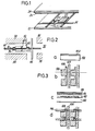
- FIG. 1 Such a structure is shown in FIG. 1. There is seen, on the one hand, a lower wall 10 carrying conductive columns 12 and conductive lines 14, a TCM 20 and a transparent electrode 22, and on the other hand, a upper wall 24 covered with a counter-electrode 26 also transparent.
- the addressing of such a device is carried out as follows.
- the lines are brought sequentially to a potential which corresponds to the gate voltage capable of making the TCM conductive.
- the video signals are applied successively to the various columns, which has the effect of exciting all the display points (or "pixels") of the line.
- FIG. 2 illustrates for example a technique described by A.J. SNELL et al. in an article entitled “Application of Amorphous Silicon Field Effect Transistors in Adressable Liquid Crystal Display Panels” published in "Applied Physics", 24, 357 - 362 (1981).
- the TCM is formed of a chrome grid G deposited on an insulating substrate 30, an amorphous silicon layer 34 (aSi), a drain D and a source S of aluminum.
- the lower armature of the capacitor is formed of a layer 38 of tin and indium oxide.
- the connection between the TCM and the armature is made by the drain D extended by a lug 40 which borrows a contact hole 42.
- the entire circuit consists of a plurality of such structures arranged in matrix form.
- the grids G are formed by connection lines 44 and the sources by columns 46.
- TCM has its source and drain contacts at the bottom and its grid at the top.
- This technique is described by M. MATSUMURA et al. in the article “Amorphous-Silicon Integrated Circuit”, published in “Proceedings of the IEEE”, vol. 68, n ° 10, October 1980, pages 1349 - 1350.
- the TCMs are located in the overlapping areas of the lines 116 and the columns 104.
- the source and the drain are respectively constituted by the appendix 108 and the part of the column 104 situated under the line 116; the control grid consists of the part of line 116 which is located between appendix 108 and column 104.
- the object of the present invention is precisely to remedy this drawback.
- the invention recommends using not one but two addressing transistors per pixel, these two transistors being connected to adjacent rows and columns.
- document GB-A-2 115 199 describes an active matrix display screen comprising a matrix of display points and, between these points, address lines and address columns, each point being connected by a MOS transistor to a line and a column.
- each point is also connected by a second transistor to the next line, but always to the same column.
- the invention proposes an improvement to this known technique by doubling the redundancy: it affects not only the rows but also the columns.
- the invention provides a particular arrangement and shape of the conductive block constituting the pixel.
- the subject of the invention is an active matrix display screen comprising a matrix of display points and, between these points, address lines (Ln) and address columns (Cn), each point (Pn, p) being connected by a thin film transistor (Tn, p) to a line (Ln) and to a column (Cn), each display point (Pn, p) consisting of a block rectangular, made of conductive material, connected to an appendage which is engaged under the addressing line corresponding to this point, and extending near the addressing column corresponding to this point, the addressing transistor (Tn, p ) of each point being located in the overlap area of the corresponding address line (Ln) with, respectively, this appendix and the corresponding column, this screen being characterized in that the rectangular block is connected to a second appendage diagonally opposite the first, engaged under the next address line e t extending near the next addressing column, a second transistor (Tn + 1, p + 1) thus being formed for the same display point, in the overlap zone
- the presence of the second TCM slightly modifies the addressing process of each pixel in the sense that the excited point Pn, p, instead of memorizing the excitation corresponding to the line Ln and to the column Cp as in art previous, will memorize the last excitation received, in this case the second (if there is no cut) which corresponds to the line Ln + 1 and to the column Cp + 1. But this modification is, in most cases, unimportant since it simply amounts to shifting the displayed image by a row interval and a column interval.
- Figure 4 shows, schematically, the principle of the active matrix display screen according to the invention.
- only two address lines are shown, of rank n and n + 1 and only two columns of rank p and p + 1. These rows and columns are denoted Ln, Ln + 1 and Cp, Cp + 1.
- a display point is identified by a double index, the first relating to the line which surmounts it and the second to the column which precedes it.
- the display point, or pixel, denoted Pn, p is the point located under the line Ln and to the right of the column Cp.
- each display point Pn, p is connected to two addressing transistors: a first transistor Tn, p which connects it to Ln and Cp and a second transistor Tn + 1, p + 1 which connects it to Ln + 1 and at Cp + 1.
- the addressing is carried out as follows.
- Pn, p When the line Ln is active, Pn, p is excited through Tn, p when the column Cp receives the appropriate video signal. But Pn, p is excited a second time when the line Ln + 1 is active and when the column Cp + 1 receives the video signal. It is therefore the second excitation which is finally memorized. There is therefore, ultimately, translation of the image of a vector equal to the diagonal of the square delimited by two adjacent lines and two adjacent columns, since the information displayed in Pn, p is in fact the information which, in the prior art, is displayed as Pn + 1, p + 1.
- the columns of the screen can be interdigitated, that is to say connected one in two to the addressing circuit by connections located either at the top or at the bottom of the screen.
- Two columns which are adjacent in one of the half addressing systems, are in fact non-adjacent in the overall system. These are, for example, columns Cn + 1, Cn + 3 or Cn and Cn + 2. In this case, the effects of the breaks in two adjacent columns are eliminated.
- each display point comprises a rectangular (or square) block 106 with two appendices 108 and 108 * which extend along two adjacent columns 114 and which engage under two adjacent lines 116.
- the first addressing transistor is in the overlapping area of a line 116 with respectively a column 114 and the first appendage 108.
- the second transistor is located in the overlapping area of the next line with respectively the second appendix 108 * and the next column.
Landscapes
- Physics & Mathematics (AREA)
- Engineering & Computer Science (AREA)
- Nonlinear Science (AREA)
- General Physics & Mathematics (AREA)
- Chemical & Material Sciences (AREA)
- Crystallography & Structural Chemistry (AREA)
- Mathematical Physics (AREA)
- Microelectronics & Electronic Packaging (AREA)
- Optics & Photonics (AREA)
- Computer Hardware Design (AREA)
- Theoretical Computer Science (AREA)
- Liquid Crystal (AREA)
- Devices For Indicating Variable Information By Combining Individual Elements (AREA)
- Liquid Crystal Display Device Control (AREA)
Applications Claiming Priority (2)
| Application Number | Priority Date | Filing Date | Title |
|---|---|---|---|
| FR8415899A FR2571913B1 (fr) | 1984-10-17 | 1984-10-17 | Ecran d'affichage a matrice active a double transistor d'adressage |
| FR8415899 | 1984-10-17 |
Publications (2)
| Publication Number | Publication Date |
|---|---|
| EP0197992A1 EP0197992A1 (fr) | 1986-10-22 |
| EP0197992B1 true EP0197992B1 (fr) | 1990-02-21 |
Family
ID=9308737
Family Applications (1)
| Application Number | Title | Priority Date | Filing Date |
|---|---|---|---|
| EP85904986A Expired - Lifetime EP0197992B1 (fr) | 1984-10-17 | 1985-10-11 | Ecran d'affichage a matrice active a double transistor d'adressage |
Country Status (7)
| Country | Link |
|---|---|
| US (1) | US5003302A (enExample) |
| EP (1) | EP0197992B1 (enExample) |
| JP (1) | JPS62500744A (enExample) |
| CA (1) | CA1261954A (enExample) |
| DE (1) | DE3576087D1 (enExample) |
| FR (1) | FR2571913B1 (enExample) |
| WO (1) | WO1986002464A1 (enExample) |
Families Citing this family (12)
| Publication number | Priority date | Publication date | Assignee | Title |
|---|---|---|---|---|
| JPS61267782A (ja) * | 1985-05-23 | 1986-11-27 | 三菱電機株式会社 | 表示素子 |
| JPH01161316A (ja) * | 1987-12-18 | 1989-06-26 | Sharp Corp | 液晶表示装置の検査方法 |
| JPH02264224A (ja) * | 1989-04-05 | 1990-10-29 | Matsushita Electric Ind Co Ltd | 点欠陥の検出および補修の可能なアクティブマトリクス基板の製造法 |
| FR2661538A1 (fr) * | 1990-04-27 | 1991-10-31 | Thomson Lcd | Ecran matriciel couleurs a definition amelioree. |
| FR2674663A1 (fr) * | 1991-03-29 | 1992-10-02 | Thomson Lcd | Ecran matriciel a definition amelioree et procede d'adressage d'un tel ecran. |
| US5302966A (en) * | 1992-06-02 | 1994-04-12 | David Sarnoff Research Center, Inc. | Active matrix electroluminescent display and method of operation |
| US6229506B1 (en) | 1997-04-23 | 2001-05-08 | Sarnoff Corporation | Active matrix light emitting diode pixel structure and concomitant method |
| JP2000310969A (ja) * | 1999-02-25 | 2000-11-07 | Canon Inc | 画像表示装置及び画像表示装置の駆動方法 |
| US7310077B2 (en) * | 2003-09-29 | 2007-12-18 | Michael Gillis Kane | Pixel circuit for an active matrix organic light-emitting diode display |
| US7633470B2 (en) | 2003-09-29 | 2009-12-15 | Michael Gillis Kane | Driver circuit, as for an OLED display |
| TWI309406B (en) * | 2005-08-24 | 2009-05-01 | Au Optronics Corp | Display panel |
| JP4483905B2 (ja) * | 2007-08-03 | 2010-06-16 | ソニー株式会社 | 表示装置および配線引き回し方法 |
Family Cites Families (9)
| Publication number | Priority date | Publication date | Assignee | Title |
|---|---|---|---|---|
| US4112333A (en) * | 1977-03-23 | 1978-09-05 | Westinghouse Electric Corp. | Display panel with integral memory capability for each display element and addressing system |
| JPS5677887A (en) * | 1979-11-30 | 1981-06-26 | Citizen Watch Co Ltd | Liquid crystal display unit |
| US4368523A (en) * | 1979-12-20 | 1983-01-11 | Tokyo Shibaura Denki Kabushiki Kaisha | Liquid crystal display device having redundant pairs of address buses |
| US4431217A (en) * | 1981-12-10 | 1984-02-14 | Fmc Corporation | Fire-safe seal for swivel joint |
| JPS58140781A (ja) * | 1982-02-17 | 1983-08-20 | 株式会社日立製作所 | 画像表示装置 |
| JPS58144888A (ja) * | 1982-02-23 | 1983-08-29 | セイコーインスツルメンツ株式会社 | 行列形液晶表示装置 |
| JPS58178321A (ja) * | 1982-04-13 | 1983-10-19 | Seiko Epson Corp | 電気光学装置 |
| FR2533072B1 (fr) * | 1982-09-14 | 1986-07-18 | Coissard Pierre | Procede de fabrication de circuits electroniques a base de transistors en couches minces et de condensateurs |
| US4641135A (en) * | 1983-12-27 | 1987-02-03 | Ncr Corporation | Field effect display system with diode selection of picture elements |
-
1984
- 1984-10-17 FR FR8415899A patent/FR2571913B1/fr not_active Expired
-
1985
- 1985-10-11 WO PCT/FR1985/000289 patent/WO1986002464A1/fr not_active Ceased
- 1985-10-11 JP JP60504478A patent/JPS62500744A/ja active Granted
- 1985-10-11 EP EP85904986A patent/EP0197992B1/fr not_active Expired - Lifetime
- 1985-10-11 US US06/882,906 patent/US5003302A/en not_active Expired - Lifetime
- 1985-10-11 DE DE8585904986T patent/DE3576087D1/de not_active Expired - Lifetime
- 1985-10-16 CA CA000493092A patent/CA1261954A/fr not_active Expired
Also Published As
| Publication number | Publication date |
|---|---|
| CA1261954A (fr) | 1989-09-26 |
| JPH0577073B2 (enExample) | 1993-10-25 |
| FR2571913B1 (fr) | 1986-12-26 |
| JPS62500744A (ja) | 1987-03-26 |
| US5003302A (en) | 1991-03-26 |
| DE3576087D1 (de) | 1990-03-29 |
| FR2571913A1 (fr) | 1986-04-18 |
| WO1986002464A1 (fr) | 1986-04-24 |
| EP0197992A1 (fr) | 1986-10-22 |
Similar Documents
| Publication | Publication Date | Title |
|---|---|---|
| EP0197992B1 (fr) | Ecran d'affichage a matrice active a double transistor d'adressage | |
| EP0103523B1 (fr) | Procédé de fabrication d'un écran d'affichage à base de transistors en couches minces et de condensateurs | |
| EP0216673B1 (fr) | Procédé de fabrication d'un transistor de commande pour écran plat de visualisation, et élément de commande réalisé selon ce procédé | |
| EP0242933A1 (fr) | Ecran d'affichage à matrice active sans transistor parasite et prcoédé de fabrication de cet écran | |
| FR2737938A1 (fr) | Dispositif d'affichage a cristaux liquides et un procede de fabrication d'un tel dispositif | |
| FR2585863A1 (fr) | Procede et structure pour dispositifs de visualisation a cristaux liquides adresses par matrice et transistors a couche mince. | |
| FR2593630A1 (fr) | Ecran d'affichage a matrice active a resistance de drain et procedes de fabrication de cet ecran | |
| EP2439583B1 (fr) | Afficheur a cristal liquide de type transmissif en technologie CMOS avec capacité de stockage auxiliaire | |
| FR2585167A1 (fr) | Structures conductrices redondantes pour affichages a cristaux liquides commandes par des transistors a effet de champ en couche mince | |
| FR2679057A1 (fr) | Structure d'ecran a cristal liquide, a matrice active et a haute definition. | |
| FR2768239A1 (fr) | Afficheur a cristaux liquides et procede de fabrication de celui-ci | |
| EP0197991B1 (fr) | Procede de fabrication de circuits electroniques a base de transistors en couches minces et de condensateurs | |
| US4643530A (en) | Reflective, thin film transistor addressed, matrix liquid crystal display | |
| EP0506528B1 (fr) | Structure de commande matricielle pour écran de visualisation | |
| EP0564337B1 (fr) | Ecran d'affichage à masque optique et procédé de réalisation de cet écran | |
| EP0485285B1 (fr) | Dispositif électrooptique bistable, écran comportant un tel dispositif et procédé de mise en oeuvre de cet écran | |
| EP0217844B1 (fr) | Procede de fabrication d'un ecran d'affichage a cristaux liquides et a reseau de diodes | |
| EP0607350B1 (fr) | Ecran Plat à Cristaux Liquides | |
| EP0186540B1 (fr) | Circuit électronique formé de transistors en couches minces pour commander un dispositif matriciel | |
| EP0368733B1 (fr) | Procédé de fabrication d'un écran d'affichage à matrice de transistors pourvus d'un masque optique | |
| FR2682492A1 (fr) | Afficheur a matrice active utilisant un plan de masse enterre. | |
| EP0688009A1 (fr) | Ecran d'affichage à matrice active à commande multiplexée | |
| FR2532116A1 (fr) | Transistor a couche mince et dispositif d'affichage a cristaux liquides utilisant ce transistor | |
| FR2602361A1 (fr) | Ecran d'affichage a matrice active sans transistor parasite et procede de fabrication de cet ecran | |
| JPH07209667A (ja) | 液晶表示装置 |
Legal Events
| Date | Code | Title | Description |
|---|---|---|---|
| PUAI | Public reference made under article 153(3) epc to a published international application that has entered the european phase |
Free format text: ORIGINAL CODE: 0009012 |
|
| 17P | Request for examination filed |
Effective date: 19860606 |
|
| AK | Designated contracting states |
Kind code of ref document: A1 Designated state(s): BE DE GB IT NL SE |
|
| 17Q | First examination report despatched |
Effective date: 19880304 |
|
| GRAA | (expected) grant |
Free format text: ORIGINAL CODE: 0009210 |
|
| AK | Designated contracting states |
Kind code of ref document: B1 Designated state(s): BE DE GB IT NL SE |
|
| REF | Corresponds to: |
Ref document number: 3576087 Country of ref document: DE Date of ref document: 19900329 |
|
| GBT | Gb: translation of ep patent filed (gb section 77(6)(a)/1977) | ||
| ITF | It: translation for a ep patent filed | ||
| PLBE | No opposition filed within time limit |
Free format text: ORIGINAL CODE: 0009261 |
|
| STAA | Information on the status of an ep patent application or granted ep patent |
Free format text: STATUS: NO OPPOSITION FILED WITHIN TIME LIMIT |
|
| 26N | No opposition filed | ||
| ITTA | It: last paid annual fee | ||
| REG | Reference to a national code |
Ref country code: GB Ref legal event code: 732E |
|
| ITPR | It: changes in ownership of a european patent |
Owner name: CESSIONE;FRANCE TELECOM |
|
| EAL | Se: european patent in force in sweden |
Ref document number: 85904986.8 |
|
| NLS | Nl: assignments of ep-patents |
Owner name: FRANCE TELECOM |
|
| REG | Reference to a national code |
Ref country code: GB Ref legal event code: IF02 |
|
| PGFP | Annual fee paid to national office [announced via postgrant information from national office to epo] |
Ref country code: SE Payment date: 20020927 Year of fee payment: 18 Ref country code: GB Payment date: 20020927 Year of fee payment: 18 |
|
| PGFP | Annual fee paid to national office [announced via postgrant information from national office to epo] |
Ref country code: NL Payment date: 20020930 Year of fee payment: 18 Ref country code: BE Payment date: 20020930 Year of fee payment: 18 |
|
| PGFP | Annual fee paid to national office [announced via postgrant information from national office to epo] |
Ref country code: DE Payment date: 20021015 Year of fee payment: 18 |
|
| PG25 | Lapsed in a contracting state [announced via postgrant information from national office to epo] |
Ref country code: GB Free format text: LAPSE BECAUSE OF NON-PAYMENT OF DUE FEES Effective date: 20031011 |
|
| PG25 | Lapsed in a contracting state [announced via postgrant information from national office to epo] |
Ref country code: SE Free format text: LAPSE BECAUSE OF NON-PAYMENT OF DUE FEES Effective date: 20031012 |
|
| PG25 | Lapsed in a contracting state [announced via postgrant information from national office to epo] |
Ref country code: BE Free format text: LAPSE BECAUSE OF NON-PAYMENT OF DUE FEES Effective date: 20031031 |
|
| BERE | Be: lapsed |
Owner name: *FRANCE TELECOM ETABLISSEMENT AUTONOME DE DROIT PU Effective date: 20031031 |
|
| PG25 | Lapsed in a contracting state [announced via postgrant information from national office to epo] |
Ref country code: NL Free format text: LAPSE BECAUSE OF NON-PAYMENT OF DUE FEES Effective date: 20040501 Ref country code: DE Free format text: LAPSE BECAUSE OF NON-PAYMENT OF DUE FEES Effective date: 20040501 |
|
| EUG | Se: european patent has lapsed | ||
| GBPC | Gb: european patent ceased through non-payment of renewal fee |
Effective date: 20031011 |
|
| NLV4 | Nl: lapsed or anulled due to non-payment of the annual fee |
Effective date: 20040501 |