EP0197627A2 - Bildverbesserungsanordnung - Google Patents
Bildverbesserungsanordnung Download PDFInfo
- Publication number
- EP0197627A2 EP0197627A2 EP86300609A EP86300609A EP0197627A2 EP 0197627 A2 EP0197627 A2 EP 0197627A2 EP 86300609 A EP86300609 A EP 86300609A EP 86300609 A EP86300609 A EP 86300609A EP 0197627 A2 EP0197627 A2 EP 0197627A2
- Authority
- EP
- European Patent Office
- Prior art keywords
- signal
- image
- enhancing
- color
- output
- Prior art date
- Legal status (The legal status is an assumption and is not a legal conclusion. Google has not performed a legal analysis and makes no representation as to the accuracy of the status listed.)
- Granted
Links
- 239000003623 enhancer Substances 0.000 title claims abstract description 22
- 230000002708 enhancing effect Effects 0.000 claims abstract description 42
- 239000002131 composite material Substances 0.000 claims abstract description 7
- 239000007787 solid Substances 0.000 claims description 8
- 238000005070 sampling Methods 0.000 description 16
- 238000006073 displacement reaction Methods 0.000 description 3
- 238000010586 diagram Methods 0.000 description 2
- 239000003086 colorant Substances 0.000 description 1
- 239000011159 matrix material Substances 0.000 description 1
- 230000004048 modification Effects 0.000 description 1
- 238000012986 modification Methods 0.000 description 1
- 238000001228 spectrum Methods 0.000 description 1
Images
Classifications
-
- H—ELECTRICITY
- H04—ELECTRIC COMMUNICATION TECHNIQUE
- H04N—PICTORIAL COMMUNICATION, e.g. TELEVISION
- H04N9/00—Details of colour television systems
- H04N9/64—Circuits for processing colour signals
- H04N9/646—Circuits for processing colour signals for image enhancement, e.g. vertical detail restoration, cross-colour elimination, contour correction, chrominance trapping filters
-
- H—ELECTRICITY
- H04—ELECTRIC COMMUNICATION TECHNIQUE
- H04N—PICTORIAL COMMUNICATION, e.g. TELEVISION
- H04N23/00—Cameras or camera modules comprising electronic image sensors; Control thereof
- H04N23/80—Camera processing pipelines; Components thereof
- H04N23/84—Camera processing pipelines; Components thereof for processing colour signals
Definitions
- This invention relates generally to an image enhancer, and more particularly is directed to an image enhancer for a color television camera having plural solid state image sensors.
- three primary color signals such as green, red and blue color signals
- a luminance signal is generated therefrom, and an image enhancing signal generated from the luminance signal is added to the luminance signal.
- the image enhancing signal generated from the luminance signal is not always a correct signal representing the edge component of the image due to the misregistrations of the three pick-up tubes.
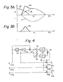
- an image enhancer in which an image enhancing signal is generated from a green primary color signal only has been proposed. Such an image enhancer is shown in Fig. 4.
- numerals 31G, 31R and 31B show input terminals to which primary color signals from pick-up tubes for green, red and blue are supplied, respectively.
- the green signal G at the input terminal 31G is phase advanced by one horizontal scanning period as to red and blue signals which are obtained at the input terminals 31R and 31B.
- the green signal G is supplied to a series circuit of delay line circuits 32 and 33 of one horizontal scanning period.
- the input signal of the delay line circuit 32 and the output signal of the delay line circuit 33 are added together by an adder 34.
- the output signal of the delay line circuit 32 is supplied to one input of a subtracter 35 while the output of the adder 34 is also supplied to another input of the subtracter 35, and the vertical edge or contour component signal is generated at the output of the subtracter 35.
- the output signal of the subtracter 35 is supplied to a low-pass-filter 37 and the bandwidth of the signal in the horizontal direction is limited thereby. And the vertical image enhancing signal is generated at the output of the low-pass-filter 37.
- the output signals of the adder 34 and the delay line circuit 32 are supplied to the adder 36. And the output signal of the adder 36 is supplied to a high-pass-filter 38 which forms twice differenciating circuit, and the horizontal image enhancing signal is obtained at the output of the high-pass-filter 38.
- the output signals of the low-pass-filter 37 and the high-pass-filter 38 are added together by an adder 39, and a composite image enhancing signal is generated at the output of the adder 39.
- the composite image enhancing signal from the adder 39 is supplied to adders 40G, 40R and 40B respectively and added to the input primary color signals. Accordingly, the image enhanced green, red and blue signals are obtained at output terminals 41G, 41R and 41B which are led out from the outputs of the adders 40G, 40R and 40B respectively.
- the above image enhancer if applied to a color television camera having three pick-up tubes, can realize a pretty good fidelity as the green signal generated from the pick-up tube has the sufficient resolution and the contribution ratio of the green signal to the luminance signal is very high.
- the above described image enhancer is applied to a color television camera having three solid state image sensors, such as CCD image sensors, for green, red and blue colors of an image of an object wherein the image of the object projected on the image sensor for green is displaced in the horizontal direction by half the alignment pitch of picture elements relative to the image of the object projected on the other image sensors for cancelling the sampling side band component centered by the sampling frequency when the image of the object is B/W or colored with low color saturation and for improving the resolution of the picture, the balance of the level of the sampling side band components is broken due to the image enhancing signal generated from the green signal, and so the object for improving the resolution can not be achieved.
- CCD image sensors three solid state image sensors
- an object of the present invention is to provide an improved image enhancer for a color television camera using solid state image sensors.
- Another object of the present invention is to provide an improved image enhancer for a color television camera using solid state image sensors, which is free from aliasing noise.
- Further object of the present invention is to provide an improved image enhancer for a color television camera using solid state image sensors, in which the sampling side band components centered by the sampling freequency of the image enhanced signals are balanced when the image of the object is B/W or colored with low color saturation.
- a vertical image enhancing signal is generated from a green signal only, an image of an object projected on the image sensor for green being displaced by half the alignment pitch of picture elements as to that projected on the other image sensors, and a horizontal image enhancing signal is generated from the equally added sum of the green signal and at least the red signal.
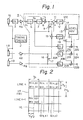
- reference numerals 1G, 1R and 1B show CCD image sensors respectively
- 2 shows a timing generator and a driver for generating common clock signal and a timing signal for driving CCD image sensors 1G, 1R and 1 B .
- Picture elements of these image sensors 1G, 1R and 1B are arranged as shown in Fig. 2.
- An alignment pitch of each of the image sensors 1G, 1R and 1B in the horizontal direction is T x and that in the vertical direction is 2 ⁇ y .
- the picture elements of the image sensors 1R and 1B are shown with this line number and the element number in the line.
- the corresponding picture elements of the image sensors 1R and 1B are located in the same spacial position with each other.
- the picture elements of the image sensor 1G are spacially displaced by 1/2 ⁇ x in the horizontal direction and 2 ⁇ y in the vertical direction relative to the corresponding picture elements of image sensors 1R and lB.
- the output signal of the image sensor 1G is phase advanced by one horizontal scanning period as to the output signals of the CCD image sensors 1R and 1B.
- the green signal G from the CCD image sensor 1G is supplied to an image enhancing circuit 5 enclosed by a broken line through a delay circuit 3 and an amplifier 4G.
- the delay circuit 3 has the delay time for compensating the phase gain due to the horizontal displacement 1/2 ⁇ x of the CCD image sensor 1G.
- the output signals, the red signal R and the blue signal B, of the image sensors 1R and 1B are supplied to the image enhancing circuit 5 enclosed by the broken line through amplifiers 4R and 4B respectively.
- the green signal G 1 from the amplifier 4G is supplied to a series circuit of delay line circuits 6 and 7 of one horizontal scannin; period and also to one input-terminal of an adder 8.
- the output signal of the delay line circuit 7 is supplied.
- the output signal of this adder 8 and the outprt signal of the delay line circuit 6 are supplied to a 3 ubtracter 11, and so the output signal of the subtracrer 11 is [2G 0 - (G 1 + G -1 )]/4.
- the vertical edge o. contour component of the image based on only the green signal is obtained from the subtracter 11.
- the output signal of the sbtracter 11 is supplied 16 to a low-pass-filter 12 for li iting the bandwidth of the signal in the horizontal diection.
- a low-pass-filter 12 for li iting the bandwidth of the signal in the horizontal diection.
- the vertical edg or contour component of the image is prevented from being mixed to the subcarrier frequency band (horizontal frequency f SC ) and the cross color can be prevented from being occurred.
- the vertical image enhancing signal VIE is generated at the output of the low-pass-filter 12.
- the horizontal image enhancing signal HIE is formed from the equally added sum of the green signal G and the added signal of the red and blue signals (R + B). This is for cancelling the aliasing noise in the image enhanced signals at the output terminals of the image enhancer, that is, because of the horizontal image enhancing signal HIE formed as described above, the sampling side band components centered by the sampling frequency which is corresponding to the alignment pitch of the picture elements, of the image enhanced signals are balanced with each other.
- the sampling side band component centered by the sampling carrier frequency (shown as one dot chain line 26 of Fig. 3A) of the output green signal G of the CCD image sensor 1G and the sampling side band component centered by the sampling carrier frequency (shown as broken line 27 of Fig. 3A) of the output red and blue signals R and B of the image sensors 1R and 1B respectively are opposite phases with each other.
- the phases of these sampling side band components are opposite with each other, if the levels of these components are equal, these components are canceled out by adding the green red and blue signals together with the proper ratio, and these side band components are prevented from being mixed to the baseband component 25 (shown as solid line of Fig. 3A).
- the image enhancing signal as shown by solid line 28 in Fig. 3A is formed from the green signal.
- the horizontal image enhancing signal is formed from the equally added sum of the green signal G and the red and blue signal (R + B) not from the green signal only. Therefore the sampling carrier of the horizontal image enhancing signal is balanced, and so the resolution of the picture can be prevented from lowering due to the sampling side band component of the image enhancing signal.
- the output signal of the variable tap 10 is supplied to an adder 15.
- the output signal of the delay line circuit 6 is supplied to an adder 21G through a delay circuit 20G
- the red signal R from the CCD image sensor 1R is supplied to an adder 21R through an amplifier 4R and a delay circuit 20R
- the blue signal B from the CCD image sensor 1B is supplied to an adder 21B through an amplifier 4B and a delay circuit 20B.
- These delay circuits 20G, 20R and 20B have the delay time for compensating the time delay caused by the low-pass-filter 12 and the high pass filter 18.
- a variable resistor 16 is connected between the outputs of the amplifiers 4R and 4B, and an output signal of a variable tap 17 of this variable resistor 16 is supplied to the adder 15.
- the output signal of the variable tap 17 which is supplied to the adder 15 is as follows,
- the coefficient S is very closed to 1 and the signal to be supplied to the adder 15 is mainly formed by the red signal.
- the sampling side band component centered by the sampling frequency is perfectly cancelled out.
- the output signal of this adder 15 is supplied to the high-pass-filter 18.
- This signal is differenciated twice in the high-pass-filter 18, and the horizontal image enhancing signal HIE is generated at the output of the high-pass-filter.
- a variable resistor 13 are connected between the outputs of the low-pass-filter 12 and the high-pass-filter 18, and a variable tap 14 of the variable resistor 13 is connected to a level adjusting circuit 19.
- a coring circuit may be arranged if necessary.
- the output signal of the level adjusting circuit 19, which is a composite image enhancing signal, is supplied to the adders 21G, 21R and 21B respectively.
- the composite image enhancing signal is added to the green signal G, the red signal R and the blue signal B from the delay circuit 20G, 20R and 20B by these adder 21G, 21R and 21B respectively.
- the image enhanced picked up signals are obtained at output terminals 22G, 22R and 22B which are led out from the outputs of the adders 21G, 21R and 21B respectively.
- the coefficient a determined by the varriable resistor 9 defines the vertical characteristics of the horizontal image enhancing signal HIE. That is, the 3elay line circuits 6 and 7, the adder 8 and the variable resistor 9 form a vertical low-pass-filter for the horizontal image enhancing signal.
- each coefficient for the green signals (Gi, Go, G -1 ) is (1/4, 0 1/4).
- the object of arranging the low-pass-filter in the vertical direction for the horizontal image enhancing signal is to prevent the crosstalk of the luminance signal to the color signal from being occurred.
- the coefficients of the green signals are (1/6, 1/6, 1/6).
- the coefficient of the red and blue signal (R + B) is 1/2, the coefficients of the signals of the successive three lines at the output of the adder 15 are (1/6, 4/6, 1/6) and therefore the response at the vertical frequency of the color subcarrier frequency is 1/3.
- the coefficients of the green signals are (1/8, 1/4, 1/8).
- the coefficients of the red and blue signal (R + B) is 1/2, the coefficients of the signals of the successive three lines at the output of the adder are (1/8, 3/4, 1/8), and therefore the response at the vertical frequency of the color subcarrier frequency is 1/2.
- the coefficients of the green signals are (0, 1/2, 0).
- the coefficient of the red and blue signal (R + B) is 1/2, the coefficients of the signals of the successive three lines at the output of the adder 15 are (0, 1, 0), and so the vertical low-pass-filter is not formed and the crosstalk of the luminance signal to the color signal is not cancelled.
- the coefficient S determines the mixing ratio of the red signal R and the blue signal B, in the prefferred example of the present invention, from the view points of the contributions of the red and blue signals to the luminance signal and the signal to noise ratio of the blue signal, the coefficient ⁇ is set to be closed to 1.
- the value of the coefficient P has no influence to the carrier balance of the output signal.
- the above embodiment is the example wherein three CCD image sensors are used, but the present invention can be applied to the color television camera in which the two CCD image sensors, one for the green signal and one for the red and blue signals are used.
Landscapes
- Engineering & Computer Science (AREA)
- Multimedia (AREA)
- Signal Processing (AREA)
- Color Television Image Signal Generators (AREA)
- Picture Signal Circuits (AREA)
- Processing Of Color Television Signals (AREA)
- Transition And Organic Metals Composition Catalysts For Addition Polymerization (AREA)
- Display Devices Of Pinball Game Machines (AREA)
- Non-Silver Salt Photosensitive Materials And Non-Silver Salt Photography (AREA)
- Pharmaceuticals Containing Other Organic And Inorganic Compounds (AREA)
- Acyclic And Carbocyclic Compounds In Medicinal Compositions (AREA)
Priority Applications (1)
| Application Number | Priority Date | Filing Date | Title |
|---|---|---|---|
| AT86300609T ATE69681T1 (de) | 1985-02-08 | 1986-01-29 | Bildverbesserungsanordnung. |
Applications Claiming Priority (2)
| Application Number | Priority Date | Filing Date | Title |
|---|---|---|---|
| JP60023293A JPH0693756B2 (ja) | 1985-02-08 | 1985-02-08 | 固体カラ−撮像装置の輪郭強調装置 |
| JP23293/85 | 1985-02-08 |
Publications (3)
| Publication Number | Publication Date |
|---|---|
| EP0197627A2 true EP0197627A2 (de) | 1986-10-15 |
| EP0197627A3 EP0197627A3 (en) | 1988-01-13 |
| EP0197627B1 EP0197627B1 (de) | 1991-11-21 |
Family
ID=12106560
Family Applications (1)
| Application Number | Title | Priority Date | Filing Date |
|---|---|---|---|
| EP86300609A Expired - Lifetime EP0197627B1 (de) | 1985-02-08 | 1986-01-29 | Bildverbesserungsanordnung |
Country Status (7)
| Country | Link |
|---|---|
| US (1) | US4672430A (de) |
| EP (1) | EP0197627B1 (de) |
| JP (1) | JPH0693756B2 (de) |
| AT (1) | ATE69681T1 (de) |
| AU (1) | AU583091B2 (de) |
| CA (1) | CA1235480A (de) |
| DE (1) | DE3682521D1 (de) |
Cited By (2)
| Publication number | Priority date | Publication date | Assignee | Title |
|---|---|---|---|---|
| WO1990009722A1 (en) * | 1989-02-13 | 1990-08-23 | Eastman Kodak Company | Detail processing method and apparatus providing uniform processing of horizontal and vertical detail components |
| WO1990015499A1 (en) * | 1989-05-30 | 1990-12-13 | Eastman Kodak Company | A color sequential optical offset image sampling system |
Families Citing this family (13)
| Publication number | Priority date | Publication date | Assignee | Title |
|---|---|---|---|---|
| JP2748373B2 (ja) * | 1987-09-29 | 1998-05-06 | ソニー株式会社 | 固体カラー撮像装置の輪郭強調装置 |
| JP2611269B2 (ja) * | 1987-10-23 | 1997-05-21 | ソニー株式会社 | 固体撮像装置の信号処理装置 |
| JP2748442B2 (ja) * | 1988-10-13 | 1998-05-06 | ソニー株式会社 | カラー映像信号の処理装置 |
| JP2789617B2 (ja) * | 1988-11-18 | 1998-08-20 | ソニー株式会社 | 固体カラー撮像装置の輪郭強調装置 |
| JP2832996B2 (ja) * | 1989-04-26 | 1998-12-09 | ソニー株式会社 | 固体カラー撮像装置の輪郭強調装置 |
| EP0410700B1 (de) * | 1989-07-25 | 1996-09-25 | Canon Kabushiki Kaisha | Bildverarbeitungsgerät |
| AU641938B2 (en) * | 1989-10-04 | 1993-10-07 | Sony Corporation | Signal processing circuit for a solid state imaging apparatus |
| JPH06169466A (ja) * | 1992-07-24 | 1994-06-14 | Matsushita Electric Ind Co Ltd | 固体撮像素子駆動装置および輪郭補正装置 |
| JPH0851635A (ja) * | 1994-08-05 | 1996-02-20 | Sony Corp | 撮像装置 |
| US5940049A (en) * | 1995-10-23 | 1999-08-17 | Polycom, Inc. | Remote interactive projector with image enhancement |
| US7409104B2 (en) * | 2002-07-18 | 2008-08-05 | .Sightic Vista Ltd | Enhanced wide dynamic range in imaging |
| JP6192391B2 (ja) * | 2013-07-05 | 2017-09-06 | キヤノン株式会社 | 光電変換システム |
| JP6160448B2 (ja) | 2013-11-05 | 2017-07-12 | ソニー株式会社 | 撮像装置および撮像装置の制御方法 |
Citations (2)
| Publication number | Priority date | Publication date | Assignee | Title |
|---|---|---|---|---|
| US4209801A (en) * | 1977-05-30 | 1980-06-24 | Rca Corporation | System for increasing the sharpness in a television picture |
| JPS5789384A (en) * | 1980-11-25 | 1982-06-03 | Hitachi Denshi Ltd | Signal processing circuit for solid color image pickup device |
Family Cites Families (7)
| Publication number | Priority date | Publication date | Assignee | Title |
|---|---|---|---|---|
| DE2018149C3 (de) * | 1970-04-16 | 1975-08-28 | Robert Bosch Gmbh, 7000 Stuttgart | Verfahren zur Erhöhung der Schärfe von Farbfernsehbildern und Schaltungsanordnung zur Durchführung des Verfahrens |
| JPS593066B2 (ja) * | 1975-09-18 | 1984-01-21 | ソニー株式会社 | コタイサツゾウタイ |
| JPS5444424A (en) * | 1977-09-14 | 1979-04-07 | Sony Corp | Solid state pick up unit |
| JPS57127375A (en) * | 1981-01-30 | 1982-08-07 | Ikegami Tsushinki Co Ltd | Vertical contour compensating circuit |
| JPS581391A (ja) * | 1981-06-26 | 1983-01-06 | Sony Corp | 固体カラー撮像装置 |
| JPS5846781A (ja) * | 1981-09-14 | 1983-03-18 | Ikegami Tsushinki Co Ltd | マゼンタ方向アパ−チヤ補正装置 |
| NL8403242A (nl) * | 1983-10-26 | 1985-05-17 | Harris Corp | Contourcorrectieschakeling voor een televisiestelsel. |
-
1985
- 1985-02-08 JP JP60023293A patent/JPH0693756B2/ja not_active Expired - Lifetime
-
1986
- 1986-01-29 DE DE8686300609T patent/DE3682521D1/de not_active Expired - Lifetime
- 1986-01-29 AT AT86300609T patent/ATE69681T1/de not_active IP Right Cessation
- 1986-01-29 EP EP86300609A patent/EP0197627B1/de not_active Expired - Lifetime
- 1986-01-31 CA CA000500811A patent/CA1235480A/en not_active Expired
- 1986-02-04 US US06/826,027 patent/US4672430A/en not_active Expired - Lifetime
- 1986-02-05 AU AU53209/86A patent/AU583091B2/en not_active Expired
Patent Citations (2)
| Publication number | Priority date | Publication date | Assignee | Title |
|---|---|---|---|---|
| US4209801A (en) * | 1977-05-30 | 1980-06-24 | Rca Corporation | System for increasing the sharpness in a television picture |
| JPS5789384A (en) * | 1980-11-25 | 1982-06-03 | Hitachi Denshi Ltd | Signal processing circuit for solid color image pickup device |
Non-Patent Citations (1)
| Title |
|---|
| PATENT ABSTRACTS OF JAPAN, vol. 6, no. 173 (E-129)[1051], 7th September 1982; & JP-A-57 089 384 (HITACHI DENSHI K.K.) 03-06-1982 * |
Cited By (2)
| Publication number | Priority date | Publication date | Assignee | Title |
|---|---|---|---|---|
| WO1990009722A1 (en) * | 1989-02-13 | 1990-08-23 | Eastman Kodak Company | Detail processing method and apparatus providing uniform processing of horizontal and vertical detail components |
| WO1990015499A1 (en) * | 1989-05-30 | 1990-12-13 | Eastman Kodak Company | A color sequential optical offset image sampling system |
Also Published As
| Publication number | Publication date |
|---|---|
| ATE69681T1 (de) | 1991-12-15 |
| AU5320986A (en) | 1986-08-14 |
| CA1235480A (en) | 1988-04-19 |
| JPH0693756B2 (ja) | 1994-11-16 |
| EP0197627A3 (en) | 1988-01-13 |
| US4672430A (en) | 1987-06-09 |
| EP0197627B1 (de) | 1991-11-21 |
| AU583091B2 (en) | 1989-04-20 |
| JPS61184057A (ja) | 1986-08-16 |
| DE3682521D1 (de) | 1992-01-02 |
Similar Documents
| Publication | Publication Date | Title |
|---|---|---|
| EP0197627A2 (de) | Bildverbesserungsanordnung | |
| EP0119862B1 (de) | Festkörperfarbabbildungsgerät | |
| US4823186A (en) | Color video signal generating device using monochrome and color image sensors having different resolutions to form a luminance signal | |
| US4716455A (en) | Chrominance signal interpolation device for a color camera | |
| US4249203A (en) | Solid state television camera | |
| US4739392A (en) | White balance adjusting apparatus having a plurality of standard color references automatically selected by the detected color temperature | |
| US4282547A (en) | Color image pick-up apparatus | |
| GB2063617A (en) | Colour filter | |
| EP0494677B1 (de) | Farbmatrixschaltung für eine CCD-Farbkamera | |
| US4205336A (en) | Signal processing system | |
| EP0164255B1 (de) | Festkörper-Farbbildaufnahmeeinrichtung | |
| US4827331A (en) | Color TV camera with circuit for adjusting the white balance of red, green, and blue signals generated from a narrow-band luminance signal and line-sequential color-difference signals | |
| EP0561409B1 (de) | Festkörperfarbbildaufnahmevorrichtung | |
| US4238765A (en) | Color television camera adapted for elimination of spurious luminance signal components | |
| EP0558338B1 (de) | Videokamera | |
| US7688362B2 (en) | Single sensor processing to obtain high resolution color component signals | |
| US5510835A (en) | Video camera having a solid-type image sensor | |
| US4527190A (en) | Mixing circuit | |
| US4236176A (en) | Luminance circuit for color television camera | |
| US4646139A (en) | Color image pickup apparatus with color filter array comprising filter elements of three different colors arranged to provide reduced folding distortion | |
| EP0483694B1 (de) | Digitale Verarbeitung für eine Farbkamera | |
| KR900006466B1 (ko) | 고체컬러 촬상장치 | |
| US3281528A (en) | Colour television system including means for separately deriving the luminance component | |
| JP2832996B2 (ja) | 固体カラー撮像装置の輪郭強調装置 | |
| EP0197767A2 (de) | Vorrichtung zum Verarbeiten eines Videosignals |
Legal Events
| Date | Code | Title | Description |
|---|---|---|---|
| PUAI | Public reference made under article 153(3) epc to a published international application that has entered the european phase |
Free format text: ORIGINAL CODE: 0009012 |
|
| 17P | Request for examination filed |
Effective date: 19860206 |
|
| AK | Designated contracting states |
Kind code of ref document: A2 Designated state(s): AT DE FR GB NL |
|
| PUAL | Search report despatched |
Free format text: ORIGINAL CODE: 0009013 |
|
| AK | Designated contracting states |
Kind code of ref document: A3 Designated state(s): AT DE FR GB NL |
|
| 17Q | First examination report despatched |
Effective date: 19900522 |
|
| GRAA | (expected) grant |
Free format text: ORIGINAL CODE: 0009210 |
|
| AK | Designated contracting states |
Kind code of ref document: B1 Designated state(s): AT DE FR GB NL |
|
| REF | Corresponds to: |
Ref document number: 69681 Country of ref document: AT Date of ref document: 19911215 Kind code of ref document: T |
|
| REF | Corresponds to: |
Ref document number: 3682521 Country of ref document: DE Date of ref document: 19920102 |
|
| ET | Fr: translation filed | ||
| PLBE | No opposition filed within time limit |
Free format text: ORIGINAL CODE: 0009261 |
|
| STAA | Information on the status of an ep patent application or granted ep patent |
Free format text: STATUS: NO OPPOSITION FILED WITHIN TIME LIMIT |
|
| 26N | No opposition filed | ||
| REG | Reference to a national code |
Ref country code: GB Ref legal event code: IF02 |
|
| PGFP | Annual fee paid to national office [announced via postgrant information from national office to epo] |
Ref country code: NL Payment date: 20050103 Year of fee payment: 20 |
|
| PGFP | Annual fee paid to national office [announced via postgrant information from national office to epo] |
Ref country code: FR Payment date: 20050110 Year of fee payment: 20 |
|
| PGFP | Annual fee paid to national office [announced via postgrant information from national office to epo] |
Ref country code: AT Payment date: 20050112 Year of fee payment: 20 |
|
| PGFP | Annual fee paid to national office [announced via postgrant information from national office to epo] |
Ref country code: GB Payment date: 20050126 Year of fee payment: 20 |
|
| PGFP | Annual fee paid to national office [announced via postgrant information from national office to epo] |
Ref country code: DE Payment date: 20050127 Year of fee payment: 20 |
|
| REG | Reference to a national code |
Ref country code: GB Ref legal event code: PE20 |
|
| PG25 | Lapsed in a contracting state [announced via postgrant information from national office to epo] |
Ref country code: GB Free format text: LAPSE BECAUSE OF EXPIRATION OF PROTECTION Effective date: 20060128 |
|
| PG25 | Lapsed in a contracting state [announced via postgrant information from national office to epo] |
Ref country code: NL Free format text: LAPSE BECAUSE OF EXPIRATION OF PROTECTION Effective date: 20060129 |
|
| NLV7 | Nl: ceased due to reaching the maximum lifetime of a patent |
Effective date: 20060129 |