EP0196474B1 - Halbleiteranordnung aus Verbindungshalbleitermaterial - Google Patents
Halbleiteranordnung aus Verbindungshalbleitermaterial Download PDFInfo
- Publication number
- EP0196474B1 EP0196474B1 EP86102757A EP86102757A EP0196474B1 EP 0196474 B1 EP0196474 B1 EP 0196474B1 EP 86102757 A EP86102757 A EP 86102757A EP 86102757 A EP86102757 A EP 86102757A EP 0196474 B1 EP0196474 B1 EP 0196474B1
- Authority
- EP
- European Patent Office
- Prior art keywords
- iso
- impurity material
- semiconductor
- electronic
- semiconductor layer
- Prior art date
- Legal status (The legal status is an assumption and is not a legal conclusion. Google has not performed a legal analysis and makes no representation as to the accuracy of the status listed.)
- Expired - Lifetime
Links
Images
Classifications
-
- H—ELECTRICITY
- H10—SEMICONDUCTOR DEVICES; ELECTRIC SOLID-STATE DEVICES NOT OTHERWISE PROVIDED FOR
- H10D—INORGANIC ELECTRIC SEMICONDUCTOR DEVICES
- H10D62/00—Semiconductor bodies, or regions thereof, of devices having potential barriers
- H10D62/80—Semiconductor bodies, or regions thereof, of devices having potential barriers characterised by the materials
- H10D62/85—Semiconductor bodies, or regions thereof, of devices having potential barriers characterised by the materials being Group III-V materials, e.g. GaAs
- H10D62/854—Semiconductor bodies, or regions thereof, of devices having potential barriers characterised by the materials being Group III-V materials, e.g. GaAs further characterised by the dopants
Definitions
- the invention relates to a method for producing a semiconductor arrangement from compound semiconductor material as is known from DE-OS 18 03 731 and the reference "Journal of Crystal Growth” 61 (1983), pages 417-424.
- Compound semiconductor material is often used in the manufacture of electronic components.
- the most common compound semiconductor materials consist of substances of III. and V. Group of the Periodic Table of the Elements, in particular of gallium arsenide or indium phosphide. Multiple connections, for example made of GaAlAs, GalnAs or GalnAsP, are also often used.
- Such semiconductor materials are used in particular to manufacture optoelectronic components, semiconductor lasers, components with Schottky junctions and integrated semiconductor circuits.
- the manufacture of the above-mentioned components is based on a base body which can be produced in various ways, for example by zone melting, by the horizontal Bridgman process or by the LEC process (Liquid Encapsulated Czochralski).
- One or more semiconductor layers are applied to this base body, preferably by epitaxial deposition.
- the dislocation density in the base body is decisive for the quality of these epitaxial semiconductor layers, which can be deposited using the liquid phase epitaxy method or vapor phase epltaxie method. For each further growing epitaxial semiconductor layer, it is of essential importance how large the dislocation density in the underlying epitaxial semiconductor layers is. Dislocation densities of 10 4 to 10 5 / cm 2 are given in the literature as relatively low. For the production of high quality components, the mentioned values are for the dislocation density however much too big. For example, for the production of field effect transistors, certain structures are built into the base body with the dislocation densities mentioned by implanting impurities. The electrical characteristic values of these field effect transistors are considerably deteriorated by the high dislocation density mentioned in the base body.
- the dislocations continuing in the epitaxial semiconductor layers also cause serious disturbances in the construction of multilayer structures with heterojunctions.
- semiconductor layers are deposited on a base body which do not have the exact same grid spacing from one another and from the base body.
- the base body often consists of a double compound semiconductor material such as gallium arsenide or indium phosphide, on which layers of ternary or quaternary semiconductor material, such as GaAlAs or GalnAsP, are deposited. Since the lattice spacing of the semiconductor materials of the different semiconductor layers does not exactly match one another, but a single-crystal growth is required, it is easy to understand that a high dislocation density in the base body has a very disruptive effect.
- the invention is based on the object of specifying a method for producing a semiconductor arrangement from compound semiconductor material, with which a multilayer semiconductor arrangement with improved properties, in particular with regard to the dislocation density, is obtained. This object is achieved by the features of claim 1.
- stress centers according to the invention By installing stress centers according to the invention in at least one semiconductor layer grown epitaxially on the base body, fixation and thus termination of the further growth of dislocations in the epitaxial semiconductor layers is achieved during their manufacture.
- These stress centers should not cause any additional, undesirable doping, which is achieved by using isoelectronic impurity material.
- the incorporation of interfering atoms that are not III. or V. group belong to the periodic table of the elements.
- the compound semiconductor material is, for example, indium phosphide, arsenic, antimony or bismuth is suitable as the isoelectronic impurity material.
- Aluminum and gallium are isoelectronic with indium, but both atoms have a smaller atomic radius than indium and are therefore not suitable for compensation of the dislocations.
- the arsenic, antimony and bismuth isoelectronic impurity materials to phosphorus have a larger atomic radius than phosphorus, so that with these elements an effective compensation of dislocations can be achieved.
- gallium arsenide or gallium phosphide the III. Group of the periodic table of the elements, in particular of indium, achieves a considerable reduction in the dislocation density, which in turn is due to the fact that indium has a larger atomic radius than that of the isoelectronic gallium to indium.
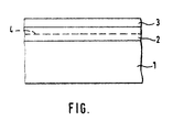
- a base body 1 which consists, for example, of indium phosphide and does not contain any isoelectronic impurity material.
- the dislocation density in this base body 1 is 10 4 - 10 5 cm -2 .
- An epitaxial layer is then applied to this base body 1 as a semiconductor layer 2, which is at least 1 ⁇ m thick and contains isoelectronic impurity material.
- the semiconductor layer 2 can also consist of ternary or quaternary material such as GalnAs or GalnAsP. In this case, antimony or bismuth is suitable as an isoelectronic impurity material.
- the isoelectronic impurity material causes a slight change in the lattice constant that is less than 10 -4 . Normally, this slight change in the lattice constant does not interfere with the further growth of epitaxial semiconductor layers. However, if - as is the case with heterojunctions - the lattice constant of the base body 1 deviates from the epitaxial layer (semiconductor layer 2) to be grown, it is advisable to add the isoelectronic impurity material to the semiconductor material of the semiconductor layer 2 such that its concentration increases with the growth of the Semiconductor layer 2, ie in the growth direction, increases. This can be done by continuously increasing the concentration of isoelectronic impurity material in the melt in liquid phase epitaxy processes.
- the semiconductor material and thus lattice constant differing from that of the semiconductor layer 2 it is advisable to add the isoelectronic impurity material to the semiconductor material for the semiconductor layer 2 such that its concentration increases with growth the semiconductor layer 2 initially increases to a maximum and then decreases again.
- the maximum of the impurity concentration of the isoelectronic impurity material is indicated in the figure by line 4. In this way it is achieved that the semiconductor layer 2 at the transitions to the base body 1 and to the semiconductor layer 3 no additional, exhibits a change in the lattice constant caused by the isoelectronic impurity material, but the dislocation density has been considerably reduced.
- the growing semiconductor layer 3 will therefore also have a low dislocation density, even if no isoelectronic impurity material has been inserted into this semiconductor layer 3 itself.
- the semiconductor layer 2 is produced by means of the liquid phase epitaxy method with a maximum of the impurity concentration of the isoelectronic impurity material, the antell of the isoelectronic impurity material in the melt will initially be continuously increased during the growth process. After reaching the maximum, the concentration of the isoelectronic impurity material will be reduced, for example, by continuously increasing the proportion of the other constituents in the melt.
- a corresponding procedure can be used in the production of the semiconductor layers by means of the gas phase epitaxy process, in which case the isoelectronic doping is carried out by supplying appropriate gaseous components.
- the proportion of the isoelectronic impurity material is preferably less than 0.5% of the element to which the impurity material is isoelectronic. Experimental experiments have shown that values between 0.1% and 0.3% are completely sufficient.
- the method according to the invention is particularly suitable for the production of optoelectronic components, laser arrangements, memory components, integrated circuits and components with Schottky contacts.
Landscapes
- Recrystallisation Techniques (AREA)
- Liquid Deposition Of Substances Of Which Semiconductor Devices Are Composed (AREA)
- Chemical Vapour Deposition (AREA)
Description
- Die Erfindung betrifft ein Verfahren zum Herstellen einer Halbleiteranordnung aus Verbindungs-Halbleitermaterial wie sie aus der DE-OS 18 03 731 und der Literaturstelle "Journal of Crystal Growth" 61 (1983), Seiten 417 - 424 bekannt ist.
- Beim Herstellen elektronischer Bauelemente wird vielfach Verbindungs-Halbleitermaterial verwendet. Die gebräuchlichsten Verbindungs-Halbleitermaterialien bestehen aus Stoffen der III. und V. Gruppe des Periodensystems der Elemente, insbesondere aus Gallium-Arsenid oder Indium-Phosphid. Vielfach werden auch Mehrfachverbindungen, beispielsweise aus GaAlAs, GalnAs oder GalnAsP verwendet. Auf der Basis solcher Halbleitermaterialien werden insbesondere optoelektronische Bauelemente, Halbleiter-Laser, Bauelemente mit Schottky-Übergängen und integrierte Halbleiterschaltungen gefertigt. Bei der Herstellung der genannten Bauelemente wird von einem Grundkörper ausgegangen, der auf verschiedene Weise, beispielsweise durch Zonenschmelzen, durch das horizontale Bridgman-Verfahren oder durch das LEC-Verfahren (Liquid Encapsulated Czochralski) hergestellt werden kann. Auf diesen Grundkörper werden eine oder mehrere Halbleiterschichten - vorzugsweise durch epitaktisches Abscheiden - aufgebracht.
- Für die Qualität dieser Epitaxie-Halbleiterschichten, die mittels Flüssigphasenepitaxie-Verfahren oder Dampfphasenepltaxie-Verfahren abgeschieden werden können, ist die Versetzungsdichte im Grundkörper entscheidend. Für jede weitere aufwachsende Epitaxie-Halbleiterschicht ist es von wesentlicher Bedeutung, wie groß die Versetzungsdichte in den darunterliegenden Epitaxie-Halbleiterschichten ist. In der Literatur werden Versetzungsdichten von 104 bis 105/cm2 als relativ niedrig angegeben. Für die Herstellung hochqualitativer Bauelemente sind die genannten Werte für die Versetzungsdichte jedoch viel zu groß. Beispielsweise zur Herstellung von Feldeffekttransistoren werden in die Grundkörper mit den genannten Versetzungsdichten durch Implantationen von Störstellen bestimmte Strukturen eingebaut. Die elektrischen Kennwerte dieser Feldeffekttransistoren werden durch die erwähnte hohe Versetzungsdichte im Grundkörper erheblich verschlechtert.
- Auch beim Aufbau von Mehrschichtstrukturen mit Hetero-Übergängen bewirken die sich in die Epitaxie-Halbleiterschichten fortsetzenden Versetzungen gravierende Störungen. Bei diesen Bauelementen werden auf einem Grundkörper Halbleiterschichten abgeschieden, die nicht den exakt gleichen Gitterabstand untereinander und zum Grundkörper aufweisen. Der Grundkörper besteht vielfach aus einem Zweifach-Verbindungs-Halbleitermaterial wie Gallium-Arsenid oder Indium-Phosphid, auf den Schichten aus ternärem oder quaternärem Halbleitermaterial, wie beispielsweise GaAlAs oder GalnAsP, abgeschieden werden. Da die Gitterabstände der Halbleitermaterialien der verschiedenen Halbleiterschichten nicht exakt miteinander übereinstimmen, aber ein einkristallines Aufwachsen gefordert wird, ist es leicht verständlich, daß sich hierbei eine hohe Versetzungsdichte im Grundkörper sehr störend auswirkt. In den genannten Epitaxie-Halbleiterschichten entstehen dann eine Vielzahl von Rekombinationszentren, durch die sich die Lebensdauer der Ladungsträger sehr stark verringert. Die Kennlinien der übergänge zwischen verschiedenen Halbleiterschichten bzw. zwischen dem Grundkörper und der darauf angeordneten Halbleiterschicht wird durch die hohe Versetzungsdichte gegenüber den ldealwerten wesentlich verschlechtert. Bei Lichtemittern bewirkt eine hohe Versetzungsdichte eine schlechte Lumineszenzausbeute, woraus sich ein geringer Wirkungsgrad von Leuchtdioden und Laseranordnungen ergibt.
- In der gattungsbildenden DE-OS 18 03 731 wird ein Verfahren zum Kristallisieren einer binären Halbleitervorrichtung beschrieben, bei dem in eine Schmelzlösung für die Kristallzucht eines binären Verbindungs-Halbleiterkristalls isoelektronische Elemente eingefügt werden. Diese Hinzugabe von isoelektronischen Elementen in die Schmelzlösung, beispielsweise von Indium in eine Gallium-Arsenid-Schmelzlösung, dient zur Homogenisierung der Schmelzlösung; die isoelektronischen Elemente sollen daher in der Schmelzlösung verbleiben und nicht in den mittels der Schmelzlösung gebildeten Verbindungs-Halbleiterkristall eingebaut werden.
- Aus der eingangs genannten Literaturstelle "Journal of Crystal Growth" 61 (1983), Seiten 417 - 424 ist es bekannt, beim Wachstum von Einkristallen aus Verbindungs-Halbleitermaterial die Schmelze mit isoelektronischem Störstellenmaterial zu dotieren, um die Materialgüte der Kristalle zu verbessern, insbesondere um die Versetzungsdichte in den Kristallen (Grundkörpern) zu reduzieren.
- Der Erfindung liegt die Aufgabe zugrunde, ein Verfahren zum Herstellen einer Halbleiteranordnung aus Verbindungs-Halbleitermaterial anzugeben, mit dem eine mehrschichtige Halbleiteranordnung mit verbesserten Eigenschaften, insbesondere bezüglich der Versetzungsdichte, erhalten wird. Diese Aufgabe wird erfindungsgemäß durch die Merkmale des Patentanspruchs 1 gelöst.
- Durch den erfindungsgemäßen Einbau von Verspannungszentren in mindestens eine auf den Grundkörper epitaktisch aufgewachsene Halbleiterschicht wird eine Fixierung und damit Beendigung des weiteren Wachstums von Versetzungen in den Epitaxie-Halbleiterschichten während deren Herstellung erreicht. Diese Verspannungszentren sollen keine zusätzliche, unerwünschte Dotierung bewirken, was durch die Verwendung isoelektronischen Störstellenmaterials erreicht wird. Hierdurch wird im Regelfalle außerdem der Einbau von Störatomen, die nicht der III. bzw. V. Gruppe des Periodensystems der Elemente angehören, erschwert. Bei der mehrschichtigen Halbleiteranordnung kann es ausreichend sein, das isoelektronische Störstellenmaterial nur in eine erste Halbleiterschicht einzubringen, die damit eine sehr geringe Versetzungsdichte von ca. 103 cm-2 und kleiner hat.
Wenn das Verbindungs-Halbleitermaterial beispielsweise Indium-Phosphid ist, eignet sich als isoelektronisches Störstellenmaterial Arsen, Antimon oder Wismut. Zum Indium ist Aluminium und Gallium isoelektronisch, doch haben beide Atome einen kleineren Atomradius als Indium und scheiden somit für eine Kompensation der Versetzungen aus. Im Gegensatz dazu weisen die zu Phosphor isoelektronischen Störstellenmaterialien Arsen, Antimon und Wismut einen größeren Atomradius als Phosphor auf, so daß mit diesen Elementen eine wirksame Kompensation der Versetzungen erreicht werden kann. Bei Gallium-Arsenid oder Gallium-Phosphid wird durch Zugabe von Störstellen der III. Gruppe des Periodensystems der Elemente, insbesondere von Indium, eine erhebliche Reduzierung der Versetzungsdichte erreicht, was wiederum darauf zurückzuführen ist, daß Indium einen größeren Atomradius als das zum Indium isoelektronische Gallium aufweist. - Bei der Anordnung nach der Figur wird von einem Grundkörper 1 ausgegangen, der beispielsweise aus Indium-Phosphid besteht und kein isoelektronisches Störstellenmaterial enthält. Die Versetzungsdichte in diesem Grundkörper 1 liegt bei 104 - 105 cm-2. Auf diesen Grundkörper 1 wird sodann eine Epitaxieschicht als Halbleiterschicht 2 aufgebracht, die mindestens 1 µm dick ist und isoelektronisches Störstellenmaterial enthält. Die Halbleiterschicht 2 kann auch aus ternärem oder quaternärem Material wie GalnAs oder GalnAsP bestehen. In diesem Fall ist Antimon bzw. Wismut als isoelektronisches Störstellenmaterial geeignet. Das isoelektronische Störstellenmaterial bewirkt eine geringfügige Änderung der Gitterkonstanten, die kleiner als 10-4 ist. Normalerweise ist diese geringfügige Änderung der Gitterkonstanten nicht störend für das weitere Aufwachsen von Epitaxie-Halbleiterschichten. Wenn jedoch - wie dies bei Hetero-Übergängen der Fall ist - die Gitterkonstante des Grundkörpers 1 von der aufzuwachsenden Epitaxieschicht (Halbleiterschicht 2) abweicht, empfiehlt es sich, dem Halbleitermaterial der Halbleiterschicht 2 das isoelektronische Störstellenmaterial so zuzusetzen, daß dessen Konzentration mit dem Wachstum der Halbleiterschicht 2, also in Aufwachsrichtung, zunimmt. Dies kann dadurch geschehen, daß bei Flüssigphasenepitaxie-Verfahren die Konzentration des isoelektronischen Störstellenmaterials in der Schmelze kontinuierlich erhöht wird.
Wenn auf die Halbleiterschicht 2 eine weitere Halbleiterschicht 3 als Epitaxieschicht aufgebracht werden soll, deren Halbleitermaterial und damit Gitterkonstante sich von der der Halbleiterschicht 2 unterscheidet, empfiehlt es sich, dem Halbleitermaterial für die Halbleiterschicht 2 das isoelektronische Störstellenmaterial so zuzusetzen, daß dessen Konzentration mit dem Wachstum der Halbleiterschicht 2 zunächst bis zu einem Maximum zunimmt und danach wieder abnimmt. Das Maximum der Störstellenkonzentration des isoelektronischen Störstellenmaterials ist in der Figur durch die Linie 4 angedeutet. Auf diese Weise wird erreicht, daß die Halbleiterschicht 2 an den übergängen zum Grundkörper 1 und zur Halbleiterschicht 3 keine zusätzliche, durch das isoelektronische Störstellenmaterial bedingte Veränderung der Gitterkonstanten aufweist, die Versetzungsdichte jedoch erheblich reduziert wurde. Die aufwachsende Halbleiterschicht 3 wird daher gleichfalls eine geringe Versetzungsdichte aufweisen, auch wenn in diese Halbleiterschicht 3 selbst kein isoelektronisches Störstellenmaterial eingefügt wurde. Bei der Herstellung der Halbleiterschicht 2 mittels Flüssigphasenepitaxie-Verfahren mit einem Maximum der Störstellenkonzentration des isoelektronischen Störstellenmaterials wird man den Antell des isoelektronischen Störstellenmaterials in der Schmelze zunächst kontinuierlich während des Aufwachsprozesses erhöhen. Nach Erreichen des Maximums wird man die Konzentration des isoelektronischen Störstellen materials beispielsweise dadurch reduzieren, daß der Anteil der anderen Bestandteile in der Schmelze kontinuierlich erhöht wird. Entsprechend kann man bei der Herstellung der Halbleiterschichten mittels Gasphasenepitaxie-Verfahren vorgehen, wobei dann die isoelektronische Dotierung durch Zufuhr entsprechender gasförmiger Komponenten erfolgt. - Der Anteil des isoelektronischen Störstellen materials beträgt vorzugsweise weniger als 0,5 % des Elementes, zu dem das Störstellenmaterial isoelektronisch ist. In experimentellen Versuchen hat sich gezeigt, daß Werte zwischen 0,1 % und 0,3 % völlig ausreichend sind.
- Das erfindungsgemäße Verfahren ist insbesondere zur Herstellung von optoelektronischen Bauelementen, Laseranordungen, Speicherbauelementen, integrierten Schaltkreisen und Bauelementen mit Schottky-Kontakten geeignet.
Claims (6)
- Verfahren zum Herstellen einer Halbleiteranordnung aus VerbindungsHalbleitermaterial, das isoelektronisches Störstellenmaterlal aus einem Element enthält, dessen Atomradius größer ist als der kovalente Atomradius des Elements des Verbindungs-Halbleitermaterials, zu dem das Störstellenmaterial isoelektronisch ist, dadurch gekennzeichnet, daß- auf einen Grundkörper (1) der kein isoelektronisches Störstellenmaterial enthält, nacheinander mehrere Halbleiterschichten (2, 3) aus unterschiedlichem Verbindungs-Halbleitermaterial zur Bildung von Hetero-Übergängen epitaktisch abgeschieden werden,- und beim Abscheidevorgang mindestens einer der Halbleiterschichten (2,3) das isoelektronische Störstellenmaterial derart zugesetzt wird, daß zur Reduzierung der Versetzungsdichte die konzentration des isoelektronischen Störstellenmaterials ausgehend von einem Hetero-Übergang, bei dem Verbindungs-Halbleitermaterialien mit unterschiedlichen Gitterkonstanten aneinandergrenzen, in Richtung auf das Innere der abzuscheidenden Halbleiterschicht zunimmt.
- Verfahren nach Anspruch 1, dadurch gekennzeichnet, daß die Konzentration des isoelektronischen Störstellenmaterials in der Halbleiterschicht (2) im Verlauf des Schichtwachstums der Halbleiterschicht (2) bis zu einem Maximum (4) zunimmt und danach wieder abnimmt.
- Verfahren nach Anspruch 1 oder 2, dadurch gekennzeichnet, daß bei einem Verbindungs-Halbleitermaterial aus Aluminium-Phosphid, Indium-Phosphid oder Gallium-Phosphid isoelektronisches Störstellenmaterial aus Elementen der V. Gruppe des Periodensystems der Elemente mit einem Atomradius größer als der von Phosphor verwendet wird.
- Verfahren nach Anspruch 3, dadurch gekennzeichnet, daß bei mindestens einer Halbleiterschicht (2, 3) aus Indium-Phosphid isoelektronisches Störstellenmaterial aus Arsen in einer Konzentration von mehr als 5 • 1018 Atome/ cm3 eingebracht worden ist.
- Verfahren nach Anspruch 1 oder 2, dadurch gekennzeichnet, daß bei einem Verbindungs-Halbleitermaterial aus Gallium-Arsenid oder Gallium-Phosphid isoelektronisches Störstellenmaterial aus Elementen der III. Gruppe des Periodensystems der Elemente mit einem Atomradius größer als der von Gallium verwendet wird.
- Verfahren nach Anspruch 1 oder 2, dadurch gekennzeichnet, daß bei einer auf einem Grundkörper (1) aus Indium-Phosphid epitaktisch abgeschiedenen Halbleiterschicht (2, 3) aus GalnAs oder GalnAsP isoelektronisches Störstellenmaterial aus Antimon oder Wismut verwendet wird.
Applications Claiming Priority (2)
| Application Number | Priority Date | Filing Date | Title |
|---|---|---|---|
| DE19853508024 DE3508024A1 (de) | 1985-03-07 | 1985-03-07 | Halbleiteranordnung aus verbindungshalbleitermaterial |
| DE3508024 | 1985-03-07 |
Publications (3)
| Publication Number | Publication Date |
|---|---|
| EP0196474A2 EP0196474A2 (de) | 1986-10-08 |
| EP0196474A3 EP0196474A3 (de) | 1989-04-05 |
| EP0196474B1 true EP0196474B1 (de) | 1997-08-06 |
Family
ID=6264417
Family Applications (1)
| Application Number | Title | Priority Date | Filing Date |
|---|---|---|---|
| EP86102757A Expired - Lifetime EP0196474B1 (de) | 1985-03-07 | 1986-03-03 | Halbleiteranordnung aus Verbindungshalbleitermaterial |
Country Status (4)
| Country | Link |
|---|---|
| US (1) | US5422731A (de) |
| EP (1) | EP0196474B1 (de) |
| JP (1) | JP2663965B2 (de) |
| DE (1) | DE3508024A1 (de) |
Families Citing this family (5)
| Publication number | Priority date | Publication date | Assignee | Title |
|---|---|---|---|---|
| US8507361B2 (en) * | 2000-11-27 | 2013-08-13 | Soitec | Fabrication of substrates with a useful layer of monocrystalline semiconductor material |
| US6815736B2 (en) * | 2001-02-09 | 2004-11-09 | Midwest Research Institute | Isoelectronic co-doping |
| GB0911134D0 (en) * | 2009-06-26 | 2009-08-12 | Univ Surrey | Optoelectronic devices |
| CA2813812C (en) | 2010-03-08 | 2016-08-23 | Alliance For Sustainable Energy, Llc | Boron, bismuth co-doping of gallium arsenide and other compounds for photonic and heterojunction bipolar transistor devices |
| DE102013002400B4 (de) | 2013-02-13 | 2018-03-29 | Otto-Von Guericke-Universität Magdeburg Technologie-Transfer-Zentrum | Vorrichtung zur Bilderfassung in Bildgebungssystemen sowie Verfahren hierfür und Verwendung |
Family Cites Families (8)
| Publication number | Priority date | Publication date | Assignee | Title |
|---|---|---|---|---|
| SE338761B (de) * | 1967-10-20 | 1971-09-20 | Philips Nv | |
| US3982261A (en) * | 1972-09-22 | 1976-09-21 | Varian Associates | Epitaxial indium-gallium-arsenide phosphide layer on lattice-matched indium-phosphide substrate and devices |
| US3958143A (en) * | 1973-01-15 | 1976-05-18 | Varian Associates | Long-wavelength photoemission cathode |
| US4237471A (en) * | 1979-06-22 | 1980-12-02 | Hamamatsu Corporation | Method of producing a semiconductor photodiode of indium antimonide and device thereof |
| US4450463A (en) * | 1981-06-29 | 1984-05-22 | Rockwell International Corporation | Multiple-quantum-layer photodetector |
| JPS60105218A (ja) * | 1983-11-11 | 1985-06-10 | Nippon Telegr & Teleph Corp <Ntt> | 3−5族化合物単結晶半導体基板 |
| JPS60176997A (ja) * | 1984-02-23 | 1985-09-11 | Sumitomo Electric Ind Ltd | 低転位密度の3−5化合物半導体単結晶 |
| JPS6185814A (ja) * | 1984-10-03 | 1986-05-01 | Nec Corp | 化合物半導体結晶ウエ−ハ |
-
1985
- 1985-03-07 DE DE19853508024 patent/DE3508024A1/de active Granted
-
1986
- 1986-03-03 EP EP86102757A patent/EP0196474B1/de not_active Expired - Lifetime
- 1986-03-06 JP JP61047480A patent/JP2663965B2/ja not_active Expired - Fee Related
-
1990
- 1990-09-12 US US07/581,413 patent/US5422731A/en not_active Expired - Fee Related
Also Published As
| Publication number | Publication date |
|---|---|
| EP0196474A3 (de) | 1989-04-05 |
| JPS61206216A (ja) | 1986-09-12 |
| EP0196474A2 (de) | 1986-10-08 |
| DE3508024C2 (de) | 1991-05-16 |
| US5422731A (en) | 1995-06-06 |
| DE3508024A1 (de) | 1986-09-11 |
| JP2663965B2 (ja) | 1997-10-15 |
Similar Documents
| Publication | Publication Date | Title |
|---|---|---|
| DE68923135T2 (de) | Verfahren zur Herstellung einer elektro-optischen Vorrichtung mit einem umgekehrten durchsichtigen Substrat. | |
| DE2231926A1 (de) | Verfahren zur herstellung von halbleitermaterial und zur herstellung von halbleitereinrichtungen | |
| DE2714945A1 (de) | Optoelektronisches halbleiter- bauelement | |
| EP1739210B1 (de) | Verfahren zur Herstellung von dotierten Halbleiter-Einkristallen, und III-V-Halbleiter-Einkristall | |
| DE69525128T2 (de) | Lichtemittierende Halbleiteranordnung und Herstellungsverfahren | |
| DE19615179B4 (de) | Verfahren zur Herstellung lichtemittierender Halbleiterbauelemente mit verbesserter Stabilität | |
| DE69232213T2 (de) | Herstellung von GaAs Bauelementen mit dotierten Gebieten und dadurch hergestellte Bauelemente | |
| DE3123234A1 (de) | "verfahren zur herstellung eines pn-uebergangs in einem halbleitermaterial der gruppe ii-vi" | |
| DE2065245B2 (de) | Elektrolumineszenz-Vorrichtung mit einem pn-übergang | |
| WO2021052635A2 (de) | Optoelektronisches bauelement, halbleiterstruktur und verfahren | |
| DE2005271B2 (de) | Epitaxialverfahren zum Aufwachsen von Halbleitermaterial auf einem dotierten Halbleitersubstrat | |
| DE3751892T2 (de) | Halbleiteranordnung mit zwei Verbindungshalbleitern und Verfahren zu ihrer Herstellung | |
| DE69107630T2 (de) | Halbleiterstruktur für optoelektronische Vorrichtung. | |
| DE2734203A1 (de) | Hetero-uebergangslaser | |
| DE2934994A1 (de) | Verfahren zur epitaktischen herstellung einer halbleiteranordnung mit mehrschichtenstruktur und anwendung dieses verfahrens | |
| DE3887790T2 (de) | Lichtemittierende Halbleitervorrichtung. | |
| EP0002658B1 (de) | Verfahren zum Herstellen einer Halbleiteranordnung | |
| DE3324220C2 (de) | Gallium-Phosphid-Leuchtdiode | |
| DE112014002691T5 (de) | Anregungsbereich, der Nanopunkte (auch als "Quantenpunkte" bezeichnet) in einem Matrixkristall umfasst, der auf Si-Substrat gezüchtet wurde und aus AlyInxGa1-y-xN-Kristall (y ≧ 0, x > 0) mit Zinkblendestruktur (auch als "kubisch" bezeichnet) besteht, und lichtemittierende Vorrichtung (LED und LD), die unter Verwendung desselben erhalten wurde | |
| DE3508024C2 (de) | ||
| DE3785859T2 (de) | Halbleiterstrukturen. | |
| DE3723222A1 (de) | Material fuer ein lichtemittierendes element und verfahren zur zuechtung von dessen kristallen | |
| DE69029687T2 (de) | Dotierungsverfahren für Halbleiterbauelemente | |
| DE69514304T2 (de) | Lichtemittierende Vorrichtung | |
| DE69207069T2 (de) | Lichtemittierende Halbleitervorrichtung |
Legal Events
| Date | Code | Title | Description |
|---|---|---|---|
| PUAI | Public reference made under article 153(3) epc to a published international application that has entered the european phase |
Free format text: ORIGINAL CODE: 0009012 |
|
| AK | Designated contracting states |
Kind code of ref document: A2 Designated state(s): FR GB IT NL |
|
| PUAL | Search report despatched |
Free format text: ORIGINAL CODE: 0009013 |
|
| RHK1 | Main classification (correction) |
Ipc: H01L 29/207 |
|
| AK | Designated contracting states |
Kind code of ref document: A3 Designated state(s): FR GB IT NL |
|
| 17P | Request for examination filed |
Effective date: 19890912 |
|
| 17Q | First examination report despatched |
Effective date: 19910124 |
|
| RAP1 | Party data changed (applicant data changed or rights of an application transferred) |
Owner name: TEMIC TELEFUNKEN MICROELECTRONIC GMBH |
|
| APAB | Appeal dossier modified |
Free format text: ORIGINAL CODE: EPIDOS NOAPE |
|
| GRAG | Despatch of communication of intention to grant |
Free format text: ORIGINAL CODE: EPIDOS AGRA |
|
| GRAH | Despatch of communication of intention to grant a patent |
Free format text: ORIGINAL CODE: EPIDOS IGRA |
|
| GRAH | Despatch of communication of intention to grant a patent |
Free format text: ORIGINAL CODE: EPIDOS IGRA |
|
| GRAA | (expected) grant |
Free format text: ORIGINAL CODE: 0009210 |
|
| AK | Designated contracting states |
Kind code of ref document: B1 Designated state(s): FR GB IT NL |
|
| GBT | Gb: translation of ep patent filed (gb section 77(6)(a)/1977) |
Effective date: 19970808 |
|
| ET | Fr: translation filed | ||
| PLBE | No opposition filed within time limit |
Free format text: ORIGINAL CODE: 0009261 |
|
| STAA | Information on the status of an ep patent application or granted ep patent |
Free format text: STATUS: NO OPPOSITION FILED WITHIN TIME LIMIT |
|
| 26N | No opposition filed | ||
| NLS | Nl: assignments of ep-patents |
Owner name: VISHAY SEMICONDUCTOR GMBH |
|
| REG | Reference to a national code |
Ref country code: GB Ref legal event code: 732E |
|
| REG | Reference to a national code |
Ref country code: FR Ref legal event code: TP |
|
| REG | Reference to a national code |
Ref country code: GB Ref legal event code: IF02 |
|
| PGFP | Annual fee paid to national office [announced via postgrant information from national office to epo] |
Ref country code: GB Payment date: 20030226 Year of fee payment: 18 |
|
| PGFP | Annual fee paid to national office [announced via postgrant information from national office to epo] |
Ref country code: NL Payment date: 20030228 Year of fee payment: 18 |
|
| PGFP | Annual fee paid to national office [announced via postgrant information from national office to epo] |
Ref country code: FR Payment date: 20030314 Year of fee payment: 18 |
|
| PG25 | Lapsed in a contracting state [announced via postgrant information from national office to epo] |
Ref country code: GB Free format text: LAPSE BECAUSE OF NON-PAYMENT OF DUE FEES Effective date: 20040303 |
|
| PG25 | Lapsed in a contracting state [announced via postgrant information from national office to epo] |
Ref country code: NL Free format text: LAPSE BECAUSE OF NON-PAYMENT OF DUE FEES Effective date: 20041001 |
|
| GBPC | Gb: european patent ceased through non-payment of renewal fee | ||
| PG25 | Lapsed in a contracting state [announced via postgrant information from national office to epo] |
Ref country code: FR Free format text: LAPSE BECAUSE OF NON-PAYMENT OF DUE FEES Effective date: 20041130 |
|
| NLV4 | Nl: lapsed or anulled due to non-payment of the annual fee |
Effective date: 20041001 |
|
| REG | Reference to a national code |
Ref country code: FR Ref legal event code: ST |
|
| PG25 | Lapsed in a contracting state [announced via postgrant information from national office to epo] |
Ref country code: IT Free format text: LAPSE BECAUSE OF NON-PAYMENT OF DUE FEES;WARNING: LAPSES OF ITALIAN PATENTS WITH EFFECTIVE DATE BEFORE 2007 MAY HAVE OCCURRED AT ANY TIME BEFORE 2007. THE CORRECT EFFECTIVE DATE MAY BE DIFFERENT FROM THE ONE RECORDED. Effective date: 20050303 |
|
| APAH | Appeal reference modified |
Free format text: ORIGINAL CODE: EPIDOSCREFNO |