EP0196245B1 - Compound semiconductor layer having high carrier concentration and method of forming same - Google Patents
Compound semiconductor layer having high carrier concentration and method of forming same Download PDFInfo
- Publication number
- EP0196245B1 EP0196245B1 EP86400366A EP86400366A EP0196245B1 EP 0196245 B1 EP0196245 B1 EP 0196245B1 EP 86400366 A EP86400366 A EP 86400366A EP 86400366 A EP86400366 A EP 86400366A EP 0196245 B1 EP0196245 B1 EP 0196245B1
- Authority
- EP
- European Patent Office
- Prior art keywords
- gaas
- layer
- concentration
- molecular beam
- compound semiconductor
- Prior art date
- Legal status (The legal status is an assumption and is not a legal conclusion. Google has not performed a legal analysis and makes no representation as to the accuracy of the status listed.)
- Expired
Links
Images


Classifications
-
- H—ELECTRICITY
- H10—SEMICONDUCTOR DEVICES; ELECTRIC SOLID-STATE DEVICES NOT OTHERWISE PROVIDED FOR
- H10D—INORGANIC ELECTRIC SEMICONDUCTOR DEVICES
- H10D30/00—Field-effect transistors [FET]
- H10D30/40—FETs having zero-dimensional [0D], one-dimensional [1D] or two-dimensional [2D] charge carrier gas channels
- H10D30/47—FETs having zero-dimensional [0D], one-dimensional [1D] or two-dimensional [2D] charge carrier gas channels having 2D charge carrier gas channels, e.g. nanoribbon FETs or high electron mobility transistors [HEMT]
- H10D30/471—High electron mobility transistors [HEMT] or high hole mobility transistors [HHMT]
- H10D30/475—High electron mobility transistors [HEMT] or high hole mobility transistors [HHMT] having wider bandgap layer formed on top of lower bandgap active layer, e.g. undoped barrier HEMTs such as i-AlGaN/GaN HEMTs
- H10D30/4755—High electron mobility transistors [HEMT] or high hole mobility transistors [HHMT] having wider bandgap layer formed on top of lower bandgap active layer, e.g. undoped barrier HEMTs such as i-AlGaN/GaN HEMTs having wide bandgap charge-carrier supplying layers, e.g. modulation doped HEMTs such as n-AlGaAs/GaAs HEMTs
-
- H—ELECTRICITY
- H01—ELECTRIC ELEMENTS
- H01L—SEMICONDUCTOR DEVICES NOT COVERED BY CLASS H10
- H01L21/00—Processes or apparatus adapted for the manufacture or treatment of semiconductor or solid state devices or of parts thereof
- H01L21/02—Manufacture or treatment of semiconductor devices or of parts thereof
- H01L21/02104—Forming layers
- H01L21/02365—Forming inorganic semiconducting materials on a substrate
- H01L21/02367—Substrates
- H01L21/0237—Materials
- H01L21/02387—Group 13/15 materials
- H01L21/02395—Arsenides
-
- H—ELECTRICITY
- H01—ELECTRIC ELEMENTS
- H01L—SEMICONDUCTOR DEVICES NOT COVERED BY CLASS H10
- H01L21/00—Processes or apparatus adapted for the manufacture or treatment of semiconductor or solid state devices or of parts thereof
- H01L21/02—Manufacture or treatment of semiconductor devices or of parts thereof
- H01L21/02104—Forming layers
- H01L21/02365—Forming inorganic semiconducting materials on a substrate
- H01L21/02436—Intermediate layers between substrates and deposited layers
- H01L21/02439—Materials
- H01L21/02455—Group 13/15 materials
- H01L21/02463—Arsenides
-
- H—ELECTRICITY
- H01—ELECTRIC ELEMENTS
- H01L—SEMICONDUCTOR DEVICES NOT COVERED BY CLASS H10
- H01L21/00—Processes or apparatus adapted for the manufacture or treatment of semiconductor or solid state devices or of parts thereof
- H01L21/02—Manufacture or treatment of semiconductor devices or of parts thereof
- H01L21/02104—Forming layers
- H01L21/02365—Forming inorganic semiconducting materials on a substrate
- H01L21/02518—Deposited layers
- H01L21/02521—Materials
- H01L21/02538—Group 13/15 materials
- H01L21/02546—Arsenides
-
- H—ELECTRICITY
- H01—ELECTRIC ELEMENTS
- H01L—SEMICONDUCTOR DEVICES NOT COVERED BY CLASS H10
- H01L21/00—Processes or apparatus adapted for the manufacture or treatment of semiconductor or solid state devices or of parts thereof
- H01L21/02—Manufacture or treatment of semiconductor devices or of parts thereof
- H01L21/02104—Forming layers
- H01L21/02365—Forming inorganic semiconducting materials on a substrate
- H01L21/02518—Deposited layers
- H01L21/0257—Doping during depositing
- H01L21/02573—Conductivity type
- H01L21/02576—N-type
-
- H—ELECTRICITY
- H01—ELECTRIC ELEMENTS
- H01L—SEMICONDUCTOR DEVICES NOT COVERED BY CLASS H10
- H01L21/00—Processes or apparatus adapted for the manufacture or treatment of semiconductor or solid state devices or of parts thereof
- H01L21/02—Manufacture or treatment of semiconductor devices or of parts thereof
- H01L21/02104—Forming layers
- H01L21/02365—Forming inorganic semiconducting materials on a substrate
- H01L21/02518—Deposited layers
- H01L21/0257—Doping during depositing
- H01L21/02573—Conductivity type
- H01L21/02579—P-type
-
- H—ELECTRICITY
- H01—ELECTRIC ELEMENTS
- H01L—SEMICONDUCTOR DEVICES NOT COVERED BY CLASS H10
- H01L21/00—Processes or apparatus adapted for the manufacture or treatment of semiconductor or solid state devices or of parts thereof
- H01L21/02—Manufacture or treatment of semiconductor devices or of parts thereof
- H01L21/02104—Forming layers
- H01L21/02365—Forming inorganic semiconducting materials on a substrate
- H01L21/02612—Formation types
- H01L21/02617—Deposition types
- H01L21/02631—Physical deposition at reduced pressure, e.g. MBE, sputtering, evaporation
-
- H—ELECTRICITY
- H10—SEMICONDUCTOR DEVICES; ELECTRIC SOLID-STATE DEVICES NOT OTHERWISE PROVIDED FOR
- H10D—INORGANIC ELECTRIC SEMICONDUCTOR DEVICES
- H10D62/00—Semiconductor bodies, or regions thereof, of devices having potential barriers
- H10D62/60—Impurity distributions or concentrations
- H10D62/605—Planar doped, e.g. atomic-plane doped or delta-doped
-
- H—ELECTRICITY
- H10—SEMICONDUCTOR DEVICES; ELECTRIC SOLID-STATE DEVICES NOT OTHERWISE PROVIDED FOR
- H10D—INORGANIC ELECTRIC SEMICONDUCTOR DEVICES
- H10D62/00—Semiconductor bodies, or regions thereof, of devices having potential barriers
- H10D62/80—Semiconductor bodies, or regions thereof, of devices having potential barriers characterised by the materials
- H10D62/85—Semiconductor bodies, or regions thereof, of devices having potential barriers characterised by the materials being Group III-V materials, e.g. GaAs
- H10D62/854—Semiconductor bodies, or regions thereof, of devices having potential barriers characterised by the materials being Group III-V materials, e.g. GaAs further characterised by the dopants
Definitions
- a compound semiconductor such as GaAs has a carrier mobility higher than that of a silicon (Si) semiconductor widely used for semiconductor devices, so a compound semiconductor contributes toward high speed operation of semiconductor devices comprising field effect transistors (FET's) or bipolar transistors. Furthermore, in an optical semiconductor device, such as a laser and a photo diode, compound semiconductors, such as GaAs and AIGaAs, are used for forming a suitable energy band condition corresponding to a desired light.
- the MBE process can be used to form (i.e., grow) a compound semiconductor layer of a semiconductor device, such as a low noise Schottky barrier GaAs FET for microwaves, a high electron mobility transistor (HEMT), and a GaAs/AIGaAs double heterojunction laser, because the MBE process can provide the device with a properties superior to those by the liquid phase epitaxy (LPE) process or vapor phase epitaxy process.
- LPE liquid phase epitaxy
- vapor phase epitaxy process vapor phase epitaxy
- a compound semiconductor layer (e.g., a GaAs layer) formed by the MBE process can be doped with a dopant by the following methods.
- the GaAs layer is grown on a GaAs substrate by bombarding the substrate with a Ga molecular beam and an As molecular beam, an Si or Be molecular beam impinges on the substrate, so that the obtained GaAs ' layer is uniformly doped with Si or Be.
- the growing and the doping are simultaneously carried out, for example, under the following conditions: a temperature of the GaAs substrate of 500° C to 700°C, a temperature of an effusion cell for As of 300° C to 400° C, a temperature of an effusion cell for Ga of 900° C to 1100°C, and a temperature of an effusion cell for Si (or Be) of 1100°C to 1350°C (or 1100°C to 1350° C).
- the doping of the dopant into the GaAs MBE layer can be carried out by a conventional ion-implantation method.
- the implanted dopant atoms are activated and crystal defects are corrected by annealing at a temperature of from 800° C to 850° C.
- the activation coefficient of implanted dopant atoms is low, so that the carrier concentration N is lower than with the above-mentioned doping manners.
- the obtained carrier electron concentration N of the GaAs layer doped with Si can attain the maximum value range of 1 x 10 1 8 - 2 x 1018 cm-3 .
- An object of the present invention is to increase a carrier concentration of a compound semiconductor (e.g., GaAs) layer.
- a compound semiconductor e.g., GaAs
- a still other object of the present invention is to improve properties of a semiconductor device comprising a compound semiconductor layer which has an increased carrier concentration, resulting in decreased resistants (e.g., a resistant of the compound semiconductor layer itself and a contact resistant) and an increased electric current.
- the above-mentioned and other objects of the present invention are attained by providing a compound semiconductor layer of GaAs or AIGaAs having atomic planes of dopant therein, each of the atomic planes having a sheet dopant concentration N sd of 2 x 10 12 cm- 2 or more and an interval between the atomic planes from each other of 6 nm or less, the carrier concentration of said GaAs or AIGaAs layer being 7 x 10 18 cm- 3 or more.
- the compound semiconductor (GaAs or AlGaAs) is formed by the MBE process and by repeated atomic plane doping in the course of the MBE growth, the atomic plane doping being carried out by using a molecular beam of a dopant at a sheet dopant concentration N sd of 2 x 1012 cm-2 or more at intervals of 6 nm or less.
- a N-type GaAs (or AlGaAs) layer incorporate Si atomic planes each of which has a sheet Si concentration N sd of 2 x 10 12 cm- 2 or more and is spaced from the next by 6 nm or less.
- the Si sheet concentration and the interval (distance between neighboring atomic planes) can be controlled so as to obtain a carrier electron concentration N of the N-type GaAs (AIGaAs) layer of 7 x 10 18 cm- 3 or more.
- an p-type GaAs (AIGaAs) layer incorporate Be atomic planes of 5 x 10 12 cm-2 or more at intervals of 4 nm or less.
- the Be sheet concentration and the interval can be controlled so as to obtain a carrier hole concentration of the P-type GaAs (AIGaAs) layer of 5 x 10 19 cm- 3 or more.
- atomic plane doping of Si into a GaAs MBE layer is carried out in the following manner.
- a (100) GaAs substrate has grown on it a GaAs layer by bombarding it with a Ga molecular beam and an As molecular beam simultaneously.
- the Ga molecular beam is stopped with the As bombardment continued, the growth of the GaAs layer is suspended and an As surface appears, as shown in Fig. 1a.
- An Si molecular beam impinges on the As surface of the growing GaAs layer, so that Si atoms occupy some of the Ga sites, as shown in Fig. 1b.
- the Si molecular beam is stopped and the Ga molecular beam is resumed, so that GaAs is grown, as shown in Fig. 1c.
- a plane comprising Si atoms is called an "atomic plane".
- this atomic plane doping is repeated and the dopant sheet concentration of each atomic plane and the interval between neighboring atomic planes are defined.
- a (100) GaAs substrate, a Ga effusion cell, an As effusion cell of Si effusion cell are set in an MBE apparatus.
- the MBE apparatus is evacuated to a high vacuum, and the substrate and the effusion cells are heated to prescribed temperature.
- substrate temperature is 520° C (500° C to 700° C)
- the Ga effusion cell temperature is 1000°C (500°C to 1100C)
- the As effusion cell temperature is 330° C (300° C to 400° C)
- the Si effusion cell temperature is 1300°C (1100°C to 1350°C).
- Each of the effusion cells is provided with a shutter which intercepts a molecular beam from the effusion cell.
- a shutter of the As effusion cell is opened to allow the As molecular beam to impinge on the GaAs substrate.
- the substrate is cleaned by the As molecular beam.
- the shutter keeps on opening to continue the bombarding of the As molecular beam (i.e., As atoms) until the end of the GaAs layer formation.
- a shutter of the Ga effusion cell is open to allow the Ga molecular beam to impinge, so that an undoped GaAs epitaxial layer (having a thickness of approximately 0.4 ⁇ m) is grown (at a growth rate of approximately 0.6 ⁇ m/h) on the substrate.
- the Ga molecular beam is stopped by closing the shutter of the Ga effusion cell to suspend the GaAs growth, and a shutter of the Si effusion cell is opened to allow the Si molecular beam to impinge on the growing GaAs layer.
- the Si atoms adhere to the As surface of the GaAs layer, as shown in Fig. 1b.
- the intensity of the Si molecular beam is controlled by adjusting the Si effusion cell temperature and the time for opening the Si cell shutter is controlled, so that the given sheet Si concentration (i.e., the prescribed number of Si atoms at an atomic plane) is attained.
- the Si cell shutter is closed and the Ga cell shutter is reopened, so that the Ga molecular beam impinges together with the As molecular beam on the GaAs layer to restart the growth of an undoped GaAs layer (having a thickness of approximately 0.1 um).
- each of the obtained GaAs MBE layers incorporates only one Si atomic plane having various sheet Si (dopant) concentrations N sd .
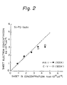
- the sheet carrier electron concentrations N s of the GaAs layers are determined by Hall measurements and capacity-voltage (C-V) measurements. The results of the measurements at 300 K (27° C) are shown in Fig. 2.
- the broken line in Fig. 2 indicates the activation coefficient of 100 %.
- Si atoms of up to 3 x 10 1 2 cm-2 are completely activated.
- the sheet Si concentration N sd increases, the sheet electron concentration N s increases, but the activation coefficient at N sd above 3 x 10 12 cm- 2 decreases and would reach a saturated value.
- a compound semiconductor MBE layer (e.g., GaAs layer) having a high carrier concentration is formed in accordance with the present invention.
- a GaAs layer doped with Si by forming 20 Si atomic planes is produced in the following manner.
- a (100) GaAs substrate is heated at approximately 520° C, and an As molecular be impinges on the substrate. These conditions are maintained.
- a Ga molecular beam impinges on the substrate to grow an undoped GaAs layer having a thickness of approximately 0.4 ⁇ m at a growth rate of approximately 0.6 ⁇ m/h.
- the Ga molecular beam is stopped to suspend the GaAs growth, and an Si molecular beam impinges on the GaAs layer to form an atomic plane.
- a sheet Si concentration N sd of the atomic plane of 2 x 10 12 cm- 2 , 3 x 10 12 cm2, or 5 x 1012 cm- 2 attained by controlling the intensity and impinging time of the Si molecular beam.
- the Si molecular beam is stopped and the Ga molecular beam reimpinges to continue growing the GaAs layer.
- the additional GaAs portion having a prescribed thickness e.g., 0.5, 1.0, 1.5, 2, 3, 4, 4.5 or 7 nm
- the Ga molecular beam is stopped to resuspend the GaAs growth.
- the above-mentioned Si atomic plane doping is repeated. Thus, alternate Si atomic doping and additional GaAs portion growth are performed.
- the final GaAs portion having a thickness of approximately 0.1 ⁇ m is grown.
- the obtained GaAs layer incorporates 20 Si atomic planes at constant intervals.
- the electron concentration N of the GaAs layer is determined by Hall measurements at 300 K. The results of the measurements are shown in Fig. 4. Solid curve lines A, B, and C indicate GaAs layers with Si atomic planes of 2 x 101 2 , 3 x 10¹², and 5 x 1012 cm- 2 , respectively. Broken curve lines indicate calculated values. As can be seen from Fig. 4, in order to obtain a GaAs MBE layer having an electron concentration N of 0.7 x 10 19 cm- 3 or more, when the sheet Si concentration N sd is 2 x 10 12, 3 x 10¹² and 5 X 1012 cm- 2 , the interval between Si atomic planes is 2.5 nm or less, 4.0 nm or less, and 6 nm or less, respectively.
- a GaAs layer doped with Be by forming 20 Be atomic planes is produced in the following manner.
- a (100) GaAs substrate has grown thereon an undoped GaAs layer (having a thickness of approximately 0.4 ⁇ m) under the same conditions as in Example 1.
- a Be molecular beam impinges on the GaAs layer to form an atomic plane having a sheet Be concentration N sd of 2 x 10 13 cm- 2 .
- the Be molecular beam is stopped and the Ga molecular beam reimpinges to continue growing the GaAs layer.
- the GaAs growth is resuspended by stopping of the Ga molecular beam.
- a prescribed thickness e.g., 0.5, 1.0, 2, 5, 10, or 20 nm
- the GaAs growth is resuspended by stopping of the Ga molecular beam.
- Such Be atomic plane doping and the additional GaAs portion growth are alternated.
- the final GaAs portion having a thickness of approximately 0.1 ⁇ m is grown.
- the obtained GaAs layer incorporates 20 Be atomic planes at constant intervals.
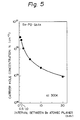
- the average hole concentration N of the GaAs layer is determined by Hall measurements at 300 K. The results of the measurements are shown in Fig. 5. As can be seen from Fig. 5.
- the hole concentration is inversely proportional to the interval between the Be atomic planes.
- the interval is 4.0 nm or less.
- the sheet Be concentration N sd reaches 2.8 x 10 20 cm- 3 . From Figs. 3 and 5, it can be concluded that when the sheet Be concentration is small, the intervals are narrowed to attain a given hole concentration N, while when the sheet Be concentration is large, the intervals are widened. Therefore, by the adoption of suitable intervals for the Be atomic planes having a sheet Be concentration of 5 x 1012 cm- 2 the given hole concentration can be attained.
- an AIGaAs MBE layer is formed in a semiconductor device utilizing a two-dimensional electron gas (2DEG), e.g., a high electron mobility transistor (HEMT), as an electron supply layer.
- 2DEG two-dimensional electron gas
- HEMT high electron mobility transistor
- a HEMT has a spacer layer of undoped AIGaAs between an undoped GaAs active layer and an electron supply layer of n-type AIGaAs.
- the undoped AIGaAs spacer layer has a thickness of 6 nm
- the n-type AIGaAs layer has a doping (Si) concentration of 2 x 10 18 cm - 3
- the sheet electron concentration of a 2DEG layer generated at the interface of undoped AIGaAs spacer layer and the GaAs active layer is 6 x 10 11 cm- 2 .
- the Si atomic plane doping technique can be applied on the undoped AIGaAs spacer layer.
- a Ga molecular beam and an AI molecular beam are stopped to suspend the AIGaAs growth.
- the Si molecular beam impinges on the AIGaAs surface to form a Si atomic plane, and then the AIGaAs growth restarted.
- the total thickness of the undoped AIGaAs layer is 12 nm and the Si atomic plane is formed at the center of the AIGaAs layer and has a sheet Si concentration of 2 x 10 12 cm-2. n this case, a sheet electron concentration of a 2DEG layer can attain to 1 x 10 12 cm- 2 .
- the Si atomic plane doping can increase the doping (dopant) amount of an AIGaAs layer for an electron supply layer.
- the average dopant (Si) concentration is further increased with result that an electric resistant of the AIGaAs layer is decreased and an electron carrier concentration is increased.
Landscapes
- Engineering & Computer Science (AREA)
- Manufacturing & Machinery (AREA)
- Physics & Mathematics (AREA)
- Condensed Matter Physics & Semiconductors (AREA)
- General Physics & Mathematics (AREA)
- Computer Hardware Design (AREA)
- Microelectronics & Electronic Packaging (AREA)
- Power Engineering (AREA)
- Materials Engineering (AREA)
- Chemical & Material Sciences (AREA)
- Physical Deposition Of Substances That Are Components Of Semiconductor Devices (AREA)
- Semiconductor Lasers (AREA)
- Junction Field-Effect Transistors (AREA)
Applications Claiming Priority (2)
| Application Number | Priority Date | Filing Date | Title |
|---|---|---|---|
| JP33862/85 | 1985-02-22 | ||
| JP60033862A JPS61216316A (ja) | 1985-02-22 | 1985-02-22 | 半導体装置の製造方法 |
Publications (2)
| Publication Number | Publication Date |
|---|---|
| EP0196245A1 EP0196245A1 (en) | 1986-10-01 |
| EP0196245B1 true EP0196245B1 (en) | 1989-10-25 |
Family
ID=12398309
Family Applications (1)
| Application Number | Title | Priority Date | Filing Date |
|---|---|---|---|
| EP86400366A Expired EP0196245B1 (en) | 1985-02-22 | 1986-02-21 | Compound semiconductor layer having high carrier concentration and method of forming same |
Country Status (4)
| Country | Link |
|---|---|
| EP (1) | EP0196245B1 (enExample) |
| JP (1) | JPS61216316A (enExample) |
| KR (1) | KR900001233B1 (enExample) |
| DE (1) | DE3666646D1 (enExample) |
Families Citing this family (6)
| Publication number | Priority date | Publication date | Assignee | Title |
|---|---|---|---|---|
| JPS6294923A (ja) * | 1985-10-22 | 1987-05-01 | Nec Corp | 半導体材料への不純物ド−ピング方法 |
| FR2620268A1 (fr) * | 1987-09-03 | 1989-03-10 | Centre Nat Rech Scient | Procede de dopage d'une couche semi-conductrice et transistor obtenu par ce procede |
| JP2586053B2 (ja) * | 1987-09-25 | 1997-02-26 | 日本電気株式会社 | 電界効果トランジスタ |
| EP0525297A3 (en) * | 1991-05-08 | 1993-10-06 | Fujitsu Limited | Method of growing doped crystal |
| US5888886A (en) * | 1997-06-30 | 1999-03-30 | Sdl, Inc. | Method of doping gan layers p-type for device fabrication |
| CN112670356B (zh) * | 2020-12-24 | 2023-05-12 | 湖南科莱特光电有限公司 | 单分子层内δ掺杂的半导体材料及其制备方法和探测器 |
Citations (1)
| Publication number | Priority date | Publication date | Assignee | Title |
|---|---|---|---|---|
| EP0183146A2 (en) * | 1984-11-19 | 1986-06-04 | Max-Planck-Gesellschaft zur Förderung der Wissenschaften e.V. | Semiconductor devices consisting of epitaxial material |
Family Cites Families (3)
| Publication number | Priority date | Publication date | Assignee | Title |
|---|---|---|---|---|
| JPS5915388B2 (ja) * | 1977-02-02 | 1984-04-09 | 株式会社日立製作所 | 半導体装置 |
| JPS5844774A (ja) * | 1981-09-11 | 1983-03-15 | Konishiroku Photo Ind Co Ltd | アモルフアスシリコン半導体装置及びその製造方法 |
| JPS57164573A (en) * | 1982-02-26 | 1982-10-09 | Hitachi Ltd | Semiconductor device |
-
1985
- 1985-02-22 JP JP60033862A patent/JPS61216316A/ja active Granted
-
1986
- 1986-02-21 EP EP86400366A patent/EP0196245B1/en not_active Expired
- 1986-02-21 DE DE8686400366T patent/DE3666646D1/de not_active Expired
- 1986-02-22 KR KR1019860001253A patent/KR900001233B1/ko not_active Expired
Patent Citations (1)
| Publication number | Priority date | Publication date | Assignee | Title |
|---|---|---|---|---|
| EP0183146A2 (en) * | 1984-11-19 | 1986-06-04 | Max-Planck-Gesellschaft zur Förderung der Wissenschaften e.V. | Semiconductor devices consisting of epitaxial material |
Also Published As
| Publication number | Publication date |
|---|---|
| DE3666646D1 (en) | 1989-11-30 |
| JPH0318733B2 (enExample) | 1991-03-13 |
| KR900001233B1 (ko) | 1990-03-05 |
| EP0196245A1 (en) | 1986-10-01 |
| JPS61216316A (ja) | 1986-09-26 |
| KR860006828A (ko) | 1986-09-15 |
Similar Documents
| Publication | Publication Date | Title |
|---|---|---|
| US5442205A (en) | Semiconductor heterostructure devices with strained semiconductor layers | |
| KR920006262B1 (ko) | 반도체 박막형성법 | |
| EP0365875B1 (en) | Capped anneal | |
| Enquist et al. | Growth and diffusion of abrupt zinc profiles in gallium arsenide and heterojunction bipolar transistor structures grown by organometallic vapor phase epitaxy | |
| US5144379A (en) | Semiconductor device having a group iii-v epitaxial semiconductor layer on a substrate | |
| US4960728A (en) | Homogenization anneal of II-VI compounds | |
| US5030580A (en) | Method for producing a silicon carbide semiconductor device | |
| EP0430562B1 (en) | Semiconductor heterostructure and method of producing the same | |
| US4489480A (en) | Method of manufacturing field effect transistors of GaAs by ion implantation | |
| US4948751A (en) | Moelcular beam epitaxy for selective epitaxial growth of III - V compound semiconductor | |
| EP0196245B1 (en) | Compound semiconductor layer having high carrier concentration and method of forming same | |
| EP0249371A2 (en) | Semiconductor device including two compound semiconductors, and method of manufacturing such a device | |
| US5227328A (en) | Method of producing epitaxial layers of II-VI semiconductors with high acceptor concentrations | |
| US5549749A (en) | Substrate with a compound semiconductor surface layer and method for preparing the same | |
| US3941624A (en) | Sn-Doped group III(a)-v(a) Ga-containing layers grown by molecular beam epitaxy | |
| EP0011898A1 (en) | Method of manufacturing a semiconductor device | |
| US4939102A (en) | Method of growing III-V semiconductor layers with high effective hole concentration | |
| EP0405832A1 (en) | Doping procedures for semiconductor devices | |
| JP2004515919A (ja) | 正極性にドープされた広い禁止帯を有する半導体の製法 | |
| JP3438116B2 (ja) | 化合物半導体装置及びその製造方法 | |
| US5183778A (en) | Method of producing a semiconductor device | |
| JP3592922B2 (ja) | 化合物半導体基板 | |
| JP2555885B2 (ja) | ゲルマニウム・砒化ガリウム接合の製造方法 | |
| JP3131929B2 (ja) | 炭素添加化合物半導体結晶成長方法 | |
| JP2705374B2 (ja) | Iii−v化合物半導体上のiv族元素半導体形成方法 |
Legal Events
| Date | Code | Title | Description |
|---|---|---|---|
| PUAI | Public reference made under article 153(3) epc to a published international application that has entered the european phase |
Free format text: ORIGINAL CODE: 0009012 |
|
| AK | Designated contracting states |
Kind code of ref document: A1 Designated state(s): DE FR GB |
|
| 17P | Request for examination filed |
Effective date: 19861017 |
|
| 17Q | First examination report despatched |
Effective date: 19880418 |
|
| GRAA | (expected) grant |
Free format text: ORIGINAL CODE: 0009210 |
|
| AK | Designated contracting states |
Kind code of ref document: B1 Designated state(s): DE FR GB |
|
| REF | Corresponds to: |
Ref document number: 3666646 Country of ref document: DE Date of ref document: 19891130 |
|
| ET | Fr: translation filed | ||
| PLBE | No opposition filed within time limit |
Free format text: ORIGINAL CODE: 0009261 |
|
| STAA | Information on the status of an ep patent application or granted ep patent |
Free format text: STATUS: NO OPPOSITION FILED WITHIN TIME LIMIT |
|
| 26N | No opposition filed | ||
| REG | Reference to a national code |
Ref country code: GB Ref legal event code: IF02 |
|
| PGFP | Annual fee paid to national office [announced via postgrant information from national office to epo] |
Ref country code: GB Payment date: 20020220 Year of fee payment: 17 |
|
| PG25 | Lapsed in a contracting state [announced via postgrant information from national office to epo] |
Ref country code: GB Free format text: LAPSE BECAUSE OF NON-PAYMENT OF DUE FEES Effective date: 20030221 |
|
| GBPC | Gb: european patent ceased through non-payment of renewal fee | ||
| PGFP | Annual fee paid to national office [announced via postgrant information from national office to epo] |
Ref country code: FR Payment date: 20050208 Year of fee payment: 20 |
|
| PGFP | Annual fee paid to national office [announced via postgrant information from national office to epo] |
Ref country code: DE Payment date: 20050217 Year of fee payment: 20 |