EP0193943B1 - Schaltungsanordnung zur Störbefreiung von Binären Datensignalen in einem digitalen Übertragungssystem - Google Patents
Schaltungsanordnung zur Störbefreiung von Binären Datensignalen in einem digitalen Übertragungssystem Download PDFInfo
- Publication number
- EP0193943B1 EP0193943B1 EP86102899A EP86102899A EP0193943B1 EP 0193943 B1 EP0193943 B1 EP 0193943B1 EP 86102899 A EP86102899 A EP 86102899A EP 86102899 A EP86102899 A EP 86102899A EP 0193943 B1 EP0193943 B1 EP 0193943B1
- Authority
- EP
- European Patent Office
- Prior art keywords
- signal
- circuit arrangement
- bistable
- output
- binary
- Prior art date
- Legal status (The legal status is an assumption and is not a legal conclusion. Google has not performed a legal analysis and makes no representation as to the accuracy of the status listed.)
- Expired
Links
- 230000005540 biological transmission Effects 0.000 title claims description 7
- 230000008030 elimination Effects 0.000 title claims description 4
- 238000003379 elimination reaction Methods 0.000 title claims description 4
- 230000001960 triggered effect Effects 0.000 claims abstract description 15
- 102100028043 Fibroblast growth factor 3 Human genes 0.000 claims description 16
- 102100024061 Integrator complex subunit 1 Human genes 0.000 claims description 16
- 101710092857 Integrator complex subunit 1 Proteins 0.000 claims description 16
- 108050002021 Integrator complex subunit 2 Proteins 0.000 claims description 16
- 230000003068 static effect Effects 0.000 claims description 4
- 230000001360 synchronised effect Effects 0.000 claims description 4
- 230000003213 activating effect Effects 0.000 claims 1
- 230000010354 integration Effects 0.000 abstract description 6
- 238000010586 diagram Methods 0.000 description 8
- 230000006870 function Effects 0.000 description 5
- 238000012545 processing Methods 0.000 description 5
- 238000000034 method Methods 0.000 description 4
- 238000005516 engineering process Methods 0.000 description 3
- 230000015654 memory Effects 0.000 description 3
- 238000011084 recovery Methods 0.000 description 3
- 230000006399 behavior Effects 0.000 description 2
- 238000013461 design Methods 0.000 description 2
- 238000011156 evaluation Methods 0.000 description 2
- 230000002452 interceptive effect Effects 0.000 description 2
- 239000003550 marker Substances 0.000 description 2
- 230000000717 retained effect Effects 0.000 description 2
- 230000001934 delay Effects 0.000 description 1
- 230000003111 delayed effect Effects 0.000 description 1
- 238000011161 development Methods 0.000 description 1
- 230000018109 developmental process Effects 0.000 description 1
- 230000009977 dual effect Effects 0.000 description 1
- 230000007257 malfunction Effects 0.000 description 1
- 239000000463 material Substances 0.000 description 1
- 230000002093 peripheral effect Effects 0.000 description 1
- 230000002441 reversible effect Effects 0.000 description 1
- 238000007493 shaping process Methods 0.000 description 1
- 238000013024 troubleshooting Methods 0.000 description 1
Images


Classifications
-
- G—PHYSICS
- G11—INFORMATION STORAGE
- G11B—INFORMATION STORAGE BASED ON RELATIVE MOVEMENT BETWEEN RECORD CARRIER AND TRANSDUCER
- G11B20/00—Signal processing not specific to the method of recording or reproducing; Circuits therefor
- G11B20/10—Digital recording or reproducing
- G11B20/10009—Improvement or modification of read or write signals
-
- G—PHYSICS
- G11—INFORMATION STORAGE
- G11B—INFORMATION STORAGE BASED ON RELATIVE MOVEMENT BETWEEN RECORD CARRIER AND TRANSDUCER
- G11B20/00—Signal processing not specific to the method of recording or reproducing; Circuits therefor
- G11B20/10—Digital recording or reproducing
- G11B20/14—Digital recording or reproducing using self-clocking codes
Definitions
- the invention relates to a circuit arrangement for interference-free binary data signals according to the preamble of claim 1.
- a large number of digital transmission systems are known for the most varied areas of application, in which the data are transmitted in the form of binary signals on the basis of one or more predefined nominal bit clock frequencies.
- the data are transmitted in the form of binary signals on the basis of one or more predefined nominal bit clock frequencies.
- causes can occur on the transmission path, in which high-frequency interference components overlap the transmitted data signals.
- An example of such a digital transmission system is e.g. B. is a data processing system with digitally working magnetic tape devices as peripheral storage.
- malfunctions are due to the fact that, for. B. dirty or worn tape material, dirty or worn heads can be used for recording.
- the typical disturbance pattern in the case of read signals from magnetic tape memories is based on a drop in the read signal amplitude in the region of an edge change, so that multiple edges then occur instead of a single edge.
- Such devices also work with a high recording density, and with the then required high resolution of the system consisting of magnetic head and magnetic layer, short interference pulses can also occur in the digitized read signal between more distant pulse edges.
- the first-mentioned form of interference elimination includes all those known measures in which the more or less smoothed edges of the data signals are converted into square wave pulses with the aid of passive filters and pulse shaping networks.
- passive filters there are limits to the use of passive filters, because unavoidable distortions are particularly unpleasant, especially in the above-mentioned application, since here, in addition to the data signals, no clock is additionally transmitted, but this must first be recovered from the data signals. It is particularly critical here that the nominal period for a bit cell can also fluctuate due to a still permissible deviation of the instantaneous belt speed from the nominal value.
- interference signal components are only very short-term compared to the useful signals, that is to say, interference signals from useful signals are discriminated on the basis of a significantly shorter pulse duration of the interference components.
- a detected edge change is only interpreted as an edge change in the useful signal if the polarity in the binary signal is retained even after a predetermined short period of time, which period is chosen to be somewhat longer than the duration of the longest possible interference signal.
- the disturbed binary data signals in a device known from JP-A 34/7852 are fed to a bistable multivibrator which acts as an pulse shaper and are converted there into signals with normal and inverted polarity.
- Each of the pulse trains thus obtained is then processed in parallel in its own circuit branch.
- An integrator is provided in each circuit branch, which is triggered by a positive edge change and integrates the subsequent pulse until the subsequent negative edge occurs. If a predetermined threshold value is exceeded, the integrator emits an output pulse of a corresponding width, which then z. B. can be differentiated.
- the differentiated signals obtained from both circuit branches are each fed to the set or reset inputs of a further bistable multivibrator which outputs the interference-free binary data signals at the output.
- this known circuit arrangement is quite capable of interfering with interfering actual edge changes of the binary data signal, i.e. to effectively suppress short-term polarity changes if the threshold value evaluating the integrated data signal is predetermined high enough to certainly cause a signal delay which is sufficient for each disturbance.
- the behavior of this circuit arrangement is more critical with regard to disturbances of the binary data signal which occur in the area of an actual pulse edge. In any case, only the last of these multiple edges is interpreted as a real edge in the binary data signal, which can lead to considerable distortions and thus to difficulties in recovering the nominal bit clock.
- the present invention is therefore based on the object of providing a circuit arrangement for interference-free binary data signals of the type mentioned at the outset, which clearly eliminates both disturbances in the area of a change of edge of the binary data signal and disturbances between further away edges, without the actual edge changes in the process binary data signal delayed too much, d. H. the data signals are distorted too much.
- the two integrators compete with one another, because in a digital transmission system, depending on the system, only one of the two integrators is activated, while the other is kept unchanged in the current state. If multiple edges occur, only one of the two integrating elements will always reach an integration value that corresponds to the predetermined threshold value. At this point in time, this is interpreted as the occurrence of an edge in the binary data signal and both integrators are reset to their initial state together.
- the bistable switching device provided at the output of the circuit is switched via its setting or. Reset input controlled. Only when the detected signal edge represents a real edge of the binary data signal does this control also switch the switching device. On the one hand, multiple edges that occur in connection with a real edge change in the binary data signal are quasi pushed together, while short dips in the binary data signal between the pulse edges are completely filtered out.
- FIG. 1 shows a section of the pulse train of disturbed binary data signals DI, which shows a typical fault pattern for read data in relation to the application in magnetic tape devices. Multiple edges can occur in the area of an edge change due to interference in the digitized signal induced in the read signal. A dip in the data signal between the further away edges is also typical.
- the second line of FIG. 1 shows the associated original binary data signal, which is free of interference and which is to be recovered from the disturbed binary data signal DI as unchanged as possible with the aid of a circuit arrangement for eliminating interference.
- the third line shows marker pulses MI triggered by the edges of the binary data signal, which are obtained from the interference-cleared pulse train of the binary data signals DO and are used, for example, in a subsequent recovery of the current bit clock that is not discussed here.
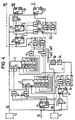
- FIG. 2 The block diagram for a circuit arrangement with which this object is achieved is shown in FIG. 2.
- data are read from a magnetic layer, for example from a magnetic tape MB, using a magnetic head MK.
- the read signals encode the intrinsic data information and are amplified in an amplifier V, possibly limited and finally digitized.
- the reading process and this signal processing is carried out in every magnetic tape device and can also be carried out here with purely commercial means. A detailed description of details is therefore unnecessary.
- the output signals of the amplifier V may be the disturbed binary data signals DI, which are supplied to the circuit arrangement for eliminating interference.
- this circuit arrangement contains two integrators INT1 and INT2 and two comparators COMP1 and COMP2, each connected to one of the integrators.
- the integrators have, as by corresponding input lines indicated, three modes of operation: "Integrate”, triggered by signals on the first input lines 11, 12, “Halt”, controlled by signals on the second input lines H1, H2 and "Reset", triggered by a signal on the third labeled R Input line.
- the two comparators COMP1, COMP2 each output an output signal on output lines AV1 and AV2. These are fed to the control logic SL and processed there in order to obtain the output signals corresponding to the interference-free binary data signals DO. B. to generate marker pulses MI.
- the polarity in the disturbed binary data signal DI changes again, so that the first integrating signal i1 is reset to the state "0".
- the first integrating element INT1 is put into the "holding" operating mode with the aid of a first hold signal h1 (FIG. 3, line i)), in which its stored value A1 does not change.
- the second integrator INT2 receives the second integrating signal i2 (FIG. 3, line j)).
- the "Integrate" operating mode for the second integrator INT2 can accordingly be found in line d) of FIG. 3, in which its current storage value A2 is shown.
- the control logic SL derives a reset signal r (line g) from FIG. 3) from this output signal of the comparator COMP1 and thus resets both integrators INT1 and INT2.
- the output signal av1 of the first comparator COMP1 in the control logic SL is interpreted as reaching an edge in the binary data signal.
- t7 both integrators are now able to evaluate a new disturbance in the binary data signal Dl.
- Such a dip in the binary data signal DI occurs at time t8 and lasts until time t9.
- the second integrating element INT2 begins to be integrated first and is set to the "hold" operating mode at time t9. Instead, the first integrator INT1 begins to integrate with the fault trailing edge and again reaches the threshold value SW at time t10.
- the corresponding output signal av1 of the first comparator COMP1 in turn triggers the functions already described in the control logic SL, the short-term dip in the binary data signal Di is interpreted as a fault, since no polarity change in the binary data signal DI has occurred after this fault has subsided. Accordingly, the state of the noise-corrected binary data signal DO shown in line b) does not change.
- FIG. 4 shows an exemplary embodiment of the circuit arrangement shown in principle in FIG. 2.
- the function of one of the integrators INTI or INT2 with the comparator COMP1 or COMP2 connected to it is realized by a first or second binary counter 1 or 2.
- the remaining circuit elements shown in Fig. 4 are essentially all attributed to the control logic SL.
- the circuit arrangement receives, as an external control signal, a clock signal CLOCK from an external clock generator 3, which is only shown schematically here.
- This clock signal hereinafter referred to simply as CL, has a frequency which corresponds to a multiple of the nominal bit clock of the binary data signals DI. It is a question of the circuit technology and also of the given application how high this frequency is actually chosen in relation to the nominal bit clock of the binary data signals. Because this frequency, as can still be seen, determines the dynamics of the circuit arrangement in cooperation with other measures. It is also indicated in FIG. 4 that a further external control signal is supplied by a schematically indicated control device 4. This control signal is a general reset signal RESET and is referred to below as RE.
- the disturbed binary data signals DI are fed to the data input of a first bistable multivibrator 5, which is triggered by the clock signal CL.
- the data input D and one of the outputs of this flip-flop are each connected to corresponding inputs of an exclusive-OR gate 6, which always emits an output signal whenever the states at the data input or data output of the first bistable flip-flop 5 are not identical, i.e. . H. an edge change has occurred in the binary data signal DI within a clock period of the clock signal CL.
- This change of state is synchronized with the aid of a second bistable multivibrator 7 in the clock pattern of the circuit arrangement.
- the output signal of this second bistable multivibrator 7 is fed to a first RS multivibrator 8, which is thereby set.
- This RS flip-flop can be configured as required, depending on the circuit technology used, and is implemented here with the help of two NAND elements.
- the static output signal of the first RS flip-flop 8 is an enable signal for the two binary counters 1, 2 in state "1". This is because two AND gates 9 and 10 are supplied in parallel, each of which receives one of the inverse output signals of the first bistable multivibrator 5 at its second inputs.
- These output signals of the first bistable multivibrator 5 correspond to the integrating signals i1 or i2 in their one state “1” and to the holding signals h1 in their inverse state “0”. or h2.
- the two binary counters 1 and 2 are constructed in a known manner as a synchronous dual counter with a predetermined maximum counter reading.
- the two binary counters 1, 2 can be implemented as four-stage Johnson counters, in which a "1" present at the data inputs is pushed through the individual stages under control of the clock signal CL and is returned to the input inverted as a carry.
- a binary "1” appears at the output of the fourth stage of the counter and a binary "0" at the output of the third stage.
- this is the maximum counter reading which then connects one of the further AND elements 11 and 12 connected downstream of these binary counters 1 and 2.
- a first edge change in the supplied disturbed binary data signal DI is recognized by the exclusive-OR gate 6, so that the first RS flip-flop 8 is set, so that the output signals of the first bistable flip-flop 5 are directed to the first and second binary counters 1 or 2 can be switched through.
- this counter e.g. B. the first binary counter 1 is heard by a count value. Since the inverse state must exist on the second binary counter 2 at the same time, the count value of this counter remains unchanged.
- this signal evaluation relates to the generation of the reset signal r.
- the outputs of the two AND gates 11 and 12 are connected to inputs of an OR gate 13, to which the general reset signal RE output by the control device 4 is also fed.
- a signal amplifier 14 is connected to the output of the OR gate 13, the output of which is in turn connected in parallel to reset inputs of the two binary counters 1 and 2 and to a reset input of the first RS flip-flop 8.
- the signal amplifier 14 therefore always issues a control signal which triggers the resetting of the two binary counters 1 and 2 and the first RS flip-flop 8 when one of the two binary counters 1 and 2 reaches the predetermined maximum count or the externally generated reset signal RE is supplied.
- the entire circuit arrangement is brought into a defined initial state, in which the first bistable multivibrator 5 is also reset.
- a renewed edge change of the binary data signal DI that occurs after the resetting of the two binary counters 1, 2 is determined immediately by the first exclusive OR element 6 and the sequence described above is started again.
- the output signals av1, av2 of the two AND gates 11 and 12 are evaluated in another form in the control logic.
- the two AND circuits 11, 12 are each connected to the setting or. connected to the reset input of a second RS flip-flop 15 constructed from NAND elements.
- This circuit detail now makes it clear what happens if, as shown in FIG. 3, a disturbance in the binary data signal occurs between times t8 and t9, which is completely filtered out.
- the second binary counter 2 be starts counting at time t8, but, unlike the first binary counter 1, does not reach the predetermined threshold value. At time t10, the maximum count in the first binary counter is reached and a set pulse is again given to the second RS flip-flop previously set.
- the further circuit elements contained in the control logic SL can serve to derive, instead of the interference-corrected binary data signals DO, data signals which in themselves contain the same information, but in a form which is better adapted to further processing of the binary data signals, for example in the recovery of the current bit clock are.
- two further bistable flip-flops 16 and 17 triggered by the clock signal CL are arranged in series at the output of the second RS flip-flop 15. Both normal outputs of these third and fourth bistable multivibrators 16 and 17 are connected to inputs of a second exclusive-OR element 18. In this way, an edge change is determined in the cleaned binary data signal.
- a corresponding output signal is fed to a fifth bistable multivibrator 19 which thereupon, controlled by the clock signal CL, outputs a marking pulse MI, as is shown in FIG. 1 without taking the signal delay into account.
- the two outputs of the third bistable multivibrator 16 and the inverse outputs of the fourth bistable multivibrator 17 are connected in pairs to the set or reset input of a third RS multivibrator 22 via two NAND elements 20 and 21, respectively.
- This third RS flip-flop 22 is therefore always set when the outputs of the third and fourth bistable flip-flops 16 and 17 connected to the NAND gate 20 both have a signal state "1". This state corresponds to a positive edge change of the noise-corrected binary data signal DO. The same applies to resetting the third RS flip-flop 22.
- the state of this RS flip-flop therefore provides information about the direction of the last edge change in the cleaned binary data signal.
- a sixth bistable multivibrator 23 triggered by the clock signal CL is finally provided, whose data input is connected to the output of the third RS multivibrator 22.
- a static edge signal FL is therefore emitted in synchronism with the marking pulse MI, the signal state of which indicates the direction of the edge that occurred last in the binary data signal.
- the marking pulse MI in connection with the edge signal FL conveys the same information in another form as the cleaned data signal DO generated at the output of the second RS flip-flop 15, but has the advantage that the information about the direction of the edge that occurred last is retained until the next edge change.
- the use of the bistable multivibrators 16, 17 and 19, 23 essentially serves the purpose of capturing the signals which occur in a clock pattern and synchronizing them with one another.
Landscapes
- Engineering & Computer Science (AREA)
- Signal Processing (AREA)
- Manipulation Of Pulses (AREA)
- Dc Digital Transmission (AREA)
- Arrangements For Transmission Of Measured Signals (AREA)
- Noise Elimination (AREA)
Priority Applications (1)
| Application Number | Priority Date | Filing Date | Title |
|---|---|---|---|
| AT86102899T ATE44185T1 (de) | 1985-03-07 | 1986-03-05 | Schaltungsanordnung zur stoerbefreiung von binaeren datensignalen in einem digitalen uebertragungssystem. |
Applications Claiming Priority (2)
| Application Number | Priority Date | Filing Date | Title |
|---|---|---|---|
| DE3508136 | 1985-03-07 | ||
| DE3508136 | 1985-03-07 |
Publications (2)
| Publication Number | Publication Date |
|---|---|
| EP0193943A1 EP0193943A1 (de) | 1986-09-10 |
| EP0193943B1 true EP0193943B1 (de) | 1989-06-21 |
Family
ID=6264508
Family Applications (1)
| Application Number | Title | Priority Date | Filing Date |
|---|---|---|---|
| EP86102899A Expired EP0193943B1 (de) | 1985-03-07 | 1986-03-05 | Schaltungsanordnung zur Störbefreiung von Binären Datensignalen in einem digitalen Übertragungssystem |
Country Status (5)
| Country | Link |
|---|---|
| US (1) | US4672635A (enExample) |
| EP (1) | EP0193943B1 (enExample) |
| JP (1) | JPS61212111A (enExample) |
| AT (1) | ATE44185T1 (enExample) |
| DE (1) | DE3664071D1 (enExample) |
Families Citing this family (5)
| Publication number | Priority date | Publication date | Assignee | Title |
|---|---|---|---|---|
| FR2634613B1 (fr) * | 1988-07-22 | 1995-07-21 | Thomson Lgt | Procede de mesure d'un palier dans un signal bruite, et appareil de mesure automatique pour la mise en oeuvre de ce procede |
| JPH04109419A (ja) * | 1990-08-29 | 1992-04-10 | Unitec Denshi Kk | ダブルアジマス4ヘッド型ビデオテープレコーダの変速再生補償装置 |
| US5737140A (en) * | 1996-06-07 | 1998-04-07 | Eastman Kodak Company | Simple pulse position modulation channel/decoder |
| EP1240054B1 (de) * | 1999-12-10 | 2005-11-16 | Continental Teves AG & Co. oHG | Schaltungsanordnung zur aktivierung eines can-bus-steuergerätes |
| CN107809225B (zh) * | 2017-11-16 | 2020-12-01 | 湖南工业大学 | 窄干扰脉冲过滤方法 |
Family Cites Families (9)
| Publication number | Priority date | Publication date | Assignee | Title |
|---|---|---|---|---|
| US3473131A (en) * | 1965-06-04 | 1969-10-14 | Radiation Inc | Level shift correction circuits |
| DE2415365C3 (de) * | 1974-03-29 | 1983-12-08 | Siemens AG, 1000 Berlin und 8000 München | Schaltungsanordnung zum Ausblenden von Impulsen, deren Dauer kürzer ist als eine vorgegebene Prüfdauer tp aus einer eingangsseitig anliegenden Folge digitaler Impulse |
| DE2549966A1 (de) * | 1975-11-07 | 1977-05-12 | Ver Flugtechnische Werke | Schaltungsanordnung zur regeneration von impulsen |
| JPS5324256A (en) * | 1976-08-19 | 1978-03-06 | Fuji Electric Co Ltd | Fulse formation circuit square signal |
| US4137504A (en) * | 1977-08-12 | 1979-01-30 | Digital Equipment Corporation | Digital filter |
| US4306194A (en) * | 1979-10-11 | 1981-12-15 | International Business Machines Corporation | Data signal detection circuit |
| FR2511566A1 (fr) * | 1981-08-12 | 1983-02-18 | Thomson Csf | Recepteur optique a seuils pour systeme de transmission numerique a debit variable |
| US4535294A (en) * | 1983-02-22 | 1985-08-13 | United Technologies Corporation | Differential receiver with self-adaptive hysteresis |
| DE3322623A1 (de) * | 1983-06-23 | 1985-01-03 | Siemens AG, 1000 Berlin und 8000 München | Schaltungsanordnung zum wiedergewinnen von in binaeren datensignalen enthaltenden daten |
-
1986
- 1986-03-05 AT AT86102899T patent/ATE44185T1/de active
- 1986-03-05 DE DE8686102899T patent/DE3664071D1/de not_active Expired
- 1986-03-05 EP EP86102899A patent/EP0193943B1/de not_active Expired
- 1986-03-06 US US06/837,001 patent/US4672635A/en not_active Expired - Fee Related
- 1986-03-07 JP JP61048740A patent/JPS61212111A/ja active Granted
Also Published As
| Publication number | Publication date |
|---|---|
| DE3664071D1 (en) | 1989-07-27 |
| JPH0355048B2 (enExample) | 1991-08-22 |
| ATE44185T1 (de) | 1989-07-15 |
| EP0193943A1 (de) | 1986-09-10 |
| JPS61212111A (ja) | 1986-09-20 |
| US4672635A (en) | 1987-06-09 |
Similar Documents
| Publication | Publication Date | Title |
|---|---|---|
| DE3544820A1 (de) | Taktfrequenzteilerschaltung | |
| CH484564A (de) | Koinzidenzgatteranordnung zum Unterdrücken zeitlich sich überschneidender Impulse | |
| DE2460979A1 (de) | Verfahren und schaltungsanordnung zur kompensation von impulsverschiebungen bei der magnetischen signalaufzeichnung | |
| DE2427225A1 (de) | Verfahren und schaltungsanordnung zur demodulation digitaler information | |
| EP0193943B1 (de) | Schaltungsanordnung zur Störbefreiung von Binären Datensignalen in einem digitalen Übertragungssystem | |
| DE2616380C3 (enExample) | ||
| DE2714219C2 (enExample) | ||
| DE2161169C2 (de) | Schaltungsanordnung zum Erzeugen von für die Fehlerlokalisierung unter n Verstärkerstellen von PCM-Übertragungsleitungen benötigten Abfragemustern | |
| DE2108320A1 (de) | Einrichtung zur Frequenz- und Phasenregelung | |
| DE2633155A1 (de) | Einrichtung zur erzeugung zeitdefinierter steuersignale | |
| EP0042961A2 (de) | Verfahren und Anordnung zur Erzeugung von Impulsen vorgegebener Zeitrelation innerhalb vorgegebener Impulsintervalle mit hoher zeitlicher Auflösung | |
| EP0019821A2 (de) | Verfahren und Anordnung zur Übertragung einer Binärfolge | |
| EP0198263A2 (de) | Schaltungsanordnung zur erdfreien Übertragung digitaler Signale über Trennstellen | |
| DE19715274A1 (de) | Gerät zum Lesen und/oder Beschreiben optischer Aufzeichnungsträger | |
| DE2710270B2 (de) | Schaltungsanordnung zur Erzeugung von mit eintreffenden Datenimpulsen synchronisierten Taktimpulsen | |
| DE2427603A1 (de) | Schaltungsanordnung zum nachbilden der wellenform von telegrafieschrittimpulsen mit digitalen mitteln | |
| DE2722981B2 (de) | Digitales Filter für binäre Signale | |
| DE3005396C2 (de) | Schaltungsanordnung zur Gewinnung eines taktgebundenen Signals | |
| DE2125380C2 (de) | Datencodierer für die Codierung von Nachrichten und Datendecodierer zum Decodieren der Nachrichten | |
| EP0062768B1 (de) | Schaltungsanordnung zur Überwachung von Schaltwerken | |
| DE2929531C2 (de) | Verfahren zur Synchronisierung zweier Datenstationen | |
| DE69303086T2 (de) | Phasen- und Frequenzkomparator | |
| DE2455652C3 (de) | Schaltungsanordnung zur Auswertung von von einem Magnetschichtspeicher gelieferten analogen Lesesignalen | |
| DE2113819C2 (de) | Fernsteuerverfahren und Vorrichtung zur Durchführung dieses Verfahrens | |
| DE2712831A1 (de) | Sprechgeschuetzter frequenzselektiver zeichenempfaenger |
Legal Events
| Date | Code | Title | Description |
|---|---|---|---|
| PUAI | Public reference made under article 153(3) epc to a published international application that has entered the european phase |
Free format text: ORIGINAL CODE: 0009012 |
|
| AK | Designated contracting states |
Kind code of ref document: A1 Designated state(s): AT CH DE FR GB IT LI NL SE |
|
| 17P | Request for examination filed |
Effective date: 19870223 |
|
| 17Q | First examination report despatched |
Effective date: 19881115 |
|
| GRAA | (expected) grant |
Free format text: ORIGINAL CODE: 0009210 |
|
| AK | Designated contracting states |
Kind code of ref document: B1 Designated state(s): AT CH DE FR GB IT LI NL SE |
|
| PG25 | Lapsed in a contracting state [announced via postgrant information from national office to epo] |
Ref country code: IT Free format text: LAPSE BECAUSE OF FAILURE TO SUBMIT A TRANSLATION OF THE DESCRIPTION OR TO PAY THE FEE WITHIN THE PRE;WARNING: LAPSES OF ITALIAN PATENTS WITH EFFECTIVE DATE BEFORE 2007 MAY HAVE OCCURRED AT ANY TIME BEFORE 2007. THE CORRECT EFFECTIVE DATE MAY BE DIFFERENT FROM THE ONE RECORDED.SCRIBED TIME-LIMIT Effective date: 19890621 Ref country code: NL Effective date: 19890621 Ref country code: SE Effective date: 19890621 |
|
| REF | Corresponds to: |
Ref document number: 44185 Country of ref document: AT Date of ref document: 19890715 Kind code of ref document: T |
|
| REF | Corresponds to: |
Ref document number: 3664071 Country of ref document: DE Date of ref document: 19890727 |
|
| ET | Fr: translation filed | ||
| GBT | Gb: translation of ep patent filed (gb section 77(6)(a)/1977) | ||
| NLV1 | Nl: lapsed or annulled due to failure to fulfill the requirements of art. 29p and 29m of the patents act | ||
| PG25 | Lapsed in a contracting state [announced via postgrant information from national office to epo] |
Ref country code: AT Effective date: 19900305 |
|
| PG25 | Lapsed in a contracting state [announced via postgrant information from national office to epo] |
Ref country code: CH Effective date: 19900331 Ref country code: LI Effective date: 19900331 |
|
| PLBE | No opposition filed within time limit |
Free format text: ORIGINAL CODE: 0009261 |
|
| STAA | Information on the status of an ep patent application or granted ep patent |
Free format text: STATUS: NO OPPOSITION FILED WITHIN TIME LIMIT |
|
| 26N | No opposition filed | ||
| REG | Reference to a national code |
Ref country code: CH Ref legal event code: PL |
|
| PGFP | Annual fee paid to national office [announced via postgrant information from national office to epo] |
Ref country code: GB Payment date: 19960220 Year of fee payment: 11 |
|
| PGFP | Annual fee paid to national office [announced via postgrant information from national office to epo] |
Ref country code: FR Payment date: 19960328 Year of fee payment: 11 |
|
| PGFP | Annual fee paid to national office [announced via postgrant information from national office to epo] |
Ref country code: DE Payment date: 19960520 Year of fee payment: 11 |
|
| PG25 | Lapsed in a contracting state [announced via postgrant information from national office to epo] |
Ref country code: GB Effective date: 19970305 |
|
| GBPC | Gb: european patent ceased through non-payment of renewal fee |
Effective date: 19970305 |
|
| PG25 | Lapsed in a contracting state [announced via postgrant information from national office to epo] |
Ref country code: FR Free format text: LAPSE BECAUSE OF NON-PAYMENT OF DUE FEES Effective date: 19971128 |
|
| PG25 | Lapsed in a contracting state [announced via postgrant information from national office to epo] |
Ref country code: DE Effective date: 19971202 |
|
| REG | Reference to a national code |
Ref country code: FR Ref legal event code: ST |