EP0193943B1 - Circuit arrangement for noise elimination in digital data signals in a digital transmission system - Google Patents
Circuit arrangement for noise elimination in digital data signals in a digital transmission system Download PDFInfo
- Publication number
- EP0193943B1 EP0193943B1 EP86102899A EP86102899A EP0193943B1 EP 0193943 B1 EP0193943 B1 EP 0193943B1 EP 86102899 A EP86102899 A EP 86102899A EP 86102899 A EP86102899 A EP 86102899A EP 0193943 B1 EP0193943 B1 EP 0193943B1
- Authority
- EP
- European Patent Office
- Prior art keywords
- signal
- circuit arrangement
- bistable
- output
- binary
- Prior art date
- Legal status (The legal status is an assumption and is not a legal conclusion. Google has not performed a legal analysis and makes no representation as to the accuracy of the status listed.)
- Expired
Links
Images


Classifications
-
- G—PHYSICS
- G11—INFORMATION STORAGE
- G11B—INFORMATION STORAGE BASED ON RELATIVE MOVEMENT BETWEEN RECORD CARRIER AND TRANSDUCER
- G11B20/00—Signal processing not specific to the method of recording or reproducing; Circuits therefor
- G11B20/10—Digital recording or reproducing
- G11B20/10009—Improvement or modification of read or write signals
-
- G—PHYSICS
- G11—INFORMATION STORAGE
- G11B—INFORMATION STORAGE BASED ON RELATIVE MOVEMENT BETWEEN RECORD CARRIER AND TRANSDUCER
- G11B20/00—Signal processing not specific to the method of recording or reproducing; Circuits therefor
- G11B20/10—Digital recording or reproducing
- G11B20/14—Digital recording or reproducing using self-clocking codes
Definitions
- the invention relates to a circuit arrangement for interference-free binary data signals according to the preamble of claim 1.
- a large number of digital transmission systems are known for the most varied areas of application, in which the data are transmitted in the form of binary signals on the basis of one or more predefined nominal bit clock frequencies.
- the data are transmitted in the form of binary signals on the basis of one or more predefined nominal bit clock frequencies.
- causes can occur on the transmission path, in which high-frequency interference components overlap the transmitted data signals.
- An example of such a digital transmission system is e.g. B. is a data processing system with digitally working magnetic tape devices as peripheral storage.
- malfunctions are due to the fact that, for. B. dirty or worn tape material, dirty or worn heads can be used for recording.
- the typical disturbance pattern in the case of read signals from magnetic tape memories is based on a drop in the read signal amplitude in the region of an edge change, so that multiple edges then occur instead of a single edge.
- Such devices also work with a high recording density, and with the then required high resolution of the system consisting of magnetic head and magnetic layer, short interference pulses can also occur in the digitized read signal between more distant pulse edges.
- the first-mentioned form of interference elimination includes all those known measures in which the more or less smoothed edges of the data signals are converted into square wave pulses with the aid of passive filters and pulse shaping networks.
- passive filters there are limits to the use of passive filters, because unavoidable distortions are particularly unpleasant, especially in the above-mentioned application, since here, in addition to the data signals, no clock is additionally transmitted, but this must first be recovered from the data signals. It is particularly critical here that the nominal period for a bit cell can also fluctuate due to a still permissible deviation of the instantaneous belt speed from the nominal value.
- interference signal components are only very short-term compared to the useful signals, that is to say, interference signals from useful signals are discriminated on the basis of a significantly shorter pulse duration of the interference components.
- a detected edge change is only interpreted as an edge change in the useful signal if the polarity in the binary signal is retained even after a predetermined short period of time, which period is chosen to be somewhat longer than the duration of the longest possible interference signal.
- the disturbed binary data signals in a device known from JP-A 34/7852 are fed to a bistable multivibrator which acts as an pulse shaper and are converted there into signals with normal and inverted polarity.
- Each of the pulse trains thus obtained is then processed in parallel in its own circuit branch.
- An integrator is provided in each circuit branch, which is triggered by a positive edge change and integrates the subsequent pulse until the subsequent negative edge occurs. If a predetermined threshold value is exceeded, the integrator emits an output pulse of a corresponding width, which then z. B. can be differentiated.
- the differentiated signals obtained from both circuit branches are each fed to the set or reset inputs of a further bistable multivibrator which outputs the interference-free binary data signals at the output.
- this known circuit arrangement is quite capable of interfering with interfering actual edge changes of the binary data signal, i.e. to effectively suppress short-term polarity changes if the threshold value evaluating the integrated data signal is predetermined high enough to certainly cause a signal delay which is sufficient for each disturbance.
- the behavior of this circuit arrangement is more critical with regard to disturbances of the binary data signal which occur in the area of an actual pulse edge. In any case, only the last of these multiple edges is interpreted as a real edge in the binary data signal, which can lead to considerable distortions and thus to difficulties in recovering the nominal bit clock.
- the present invention is therefore based on the object of providing a circuit arrangement for interference-free binary data signals of the type mentioned at the outset, which clearly eliminates both disturbances in the area of a change of edge of the binary data signal and disturbances between further away edges, without the actual edge changes in the process binary data signal delayed too much, d. H. the data signals are distorted too much.
- the two integrators compete with one another, because in a digital transmission system, depending on the system, only one of the two integrators is activated, while the other is kept unchanged in the current state. If multiple edges occur, only one of the two integrating elements will always reach an integration value that corresponds to the predetermined threshold value. At this point in time, this is interpreted as the occurrence of an edge in the binary data signal and both integrators are reset to their initial state together.
- the bistable switching device provided at the output of the circuit is switched via its setting or. Reset input controlled. Only when the detected signal edge represents a real edge of the binary data signal does this control also switch the switching device. On the one hand, multiple edges that occur in connection with a real edge change in the binary data signal are quasi pushed together, while short dips in the binary data signal between the pulse edges are completely filtered out.
- FIG. 1 shows a section of the pulse train of disturbed binary data signals DI, which shows a typical fault pattern for read data in relation to the application in magnetic tape devices. Multiple edges can occur in the area of an edge change due to interference in the digitized signal induced in the read signal. A dip in the data signal between the further away edges is also typical.
- the second line of FIG. 1 shows the associated original binary data signal, which is free of interference and which is to be recovered from the disturbed binary data signal DI as unchanged as possible with the aid of a circuit arrangement for eliminating interference.
- the third line shows marker pulses MI triggered by the edges of the binary data signal, which are obtained from the interference-cleared pulse train of the binary data signals DO and are used, for example, in a subsequent recovery of the current bit clock that is not discussed here.
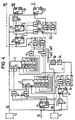
- FIG. 2 The block diagram for a circuit arrangement with which this object is achieved is shown in FIG. 2.
- data are read from a magnetic layer, for example from a magnetic tape MB, using a magnetic head MK.
- the read signals encode the intrinsic data information and are amplified in an amplifier V, possibly limited and finally digitized.
- the reading process and this signal processing is carried out in every magnetic tape device and can also be carried out here with purely commercial means. A detailed description of details is therefore unnecessary.
- the output signals of the amplifier V may be the disturbed binary data signals DI, which are supplied to the circuit arrangement for eliminating interference.
- this circuit arrangement contains two integrators INT1 and INT2 and two comparators COMP1 and COMP2, each connected to one of the integrators.
- the integrators have, as by corresponding input lines indicated, three modes of operation: "Integrate”, triggered by signals on the first input lines 11, 12, “Halt”, controlled by signals on the second input lines H1, H2 and "Reset", triggered by a signal on the third labeled R Input line.
- the two comparators COMP1, COMP2 each output an output signal on output lines AV1 and AV2. These are fed to the control logic SL and processed there in order to obtain the output signals corresponding to the interference-free binary data signals DO. B. to generate marker pulses MI.
- the polarity in the disturbed binary data signal DI changes again, so that the first integrating signal i1 is reset to the state "0".
- the first integrating element INT1 is put into the "holding" operating mode with the aid of a first hold signal h1 (FIG. 3, line i)), in which its stored value A1 does not change.
- the second integrator INT2 receives the second integrating signal i2 (FIG. 3, line j)).
- the "Integrate" operating mode for the second integrator INT2 can accordingly be found in line d) of FIG. 3, in which its current storage value A2 is shown.
- the control logic SL derives a reset signal r (line g) from FIG. 3) from this output signal of the comparator COMP1 and thus resets both integrators INT1 and INT2.
- the output signal av1 of the first comparator COMP1 in the control logic SL is interpreted as reaching an edge in the binary data signal.
- t7 both integrators are now able to evaluate a new disturbance in the binary data signal Dl.
- Such a dip in the binary data signal DI occurs at time t8 and lasts until time t9.
- the second integrating element INT2 begins to be integrated first and is set to the "hold" operating mode at time t9. Instead, the first integrator INT1 begins to integrate with the fault trailing edge and again reaches the threshold value SW at time t10.
- the corresponding output signal av1 of the first comparator COMP1 in turn triggers the functions already described in the control logic SL, the short-term dip in the binary data signal Di is interpreted as a fault, since no polarity change in the binary data signal DI has occurred after this fault has subsided. Accordingly, the state of the noise-corrected binary data signal DO shown in line b) does not change.
- FIG. 4 shows an exemplary embodiment of the circuit arrangement shown in principle in FIG. 2.
- the function of one of the integrators INTI or INT2 with the comparator COMP1 or COMP2 connected to it is realized by a first or second binary counter 1 or 2.
- the remaining circuit elements shown in Fig. 4 are essentially all attributed to the control logic SL.
- the circuit arrangement receives, as an external control signal, a clock signal CLOCK from an external clock generator 3, which is only shown schematically here.
- This clock signal hereinafter referred to simply as CL, has a frequency which corresponds to a multiple of the nominal bit clock of the binary data signals DI. It is a question of the circuit technology and also of the given application how high this frequency is actually chosen in relation to the nominal bit clock of the binary data signals. Because this frequency, as can still be seen, determines the dynamics of the circuit arrangement in cooperation with other measures. It is also indicated in FIG. 4 that a further external control signal is supplied by a schematically indicated control device 4. This control signal is a general reset signal RESET and is referred to below as RE.
- the disturbed binary data signals DI are fed to the data input of a first bistable multivibrator 5, which is triggered by the clock signal CL.
- the data input D and one of the outputs of this flip-flop are each connected to corresponding inputs of an exclusive-OR gate 6, which always emits an output signal whenever the states at the data input or data output of the first bistable flip-flop 5 are not identical, i.e. . H. an edge change has occurred in the binary data signal DI within a clock period of the clock signal CL.
- This change of state is synchronized with the aid of a second bistable multivibrator 7 in the clock pattern of the circuit arrangement.
- the output signal of this second bistable multivibrator 7 is fed to a first RS multivibrator 8, which is thereby set.
- This RS flip-flop can be configured as required, depending on the circuit technology used, and is implemented here with the help of two NAND elements.
- the static output signal of the first RS flip-flop 8 is an enable signal for the two binary counters 1, 2 in state "1". This is because two AND gates 9 and 10 are supplied in parallel, each of which receives one of the inverse output signals of the first bistable multivibrator 5 at its second inputs.
- These output signals of the first bistable multivibrator 5 correspond to the integrating signals i1 or i2 in their one state “1” and to the holding signals h1 in their inverse state “0”. or h2.
- the two binary counters 1 and 2 are constructed in a known manner as a synchronous dual counter with a predetermined maximum counter reading.
- the two binary counters 1, 2 can be implemented as four-stage Johnson counters, in which a "1" present at the data inputs is pushed through the individual stages under control of the clock signal CL and is returned to the input inverted as a carry.
- a binary "1” appears at the output of the fourth stage of the counter and a binary "0" at the output of the third stage.
- this is the maximum counter reading which then connects one of the further AND elements 11 and 12 connected downstream of these binary counters 1 and 2.
- a first edge change in the supplied disturbed binary data signal DI is recognized by the exclusive-OR gate 6, so that the first RS flip-flop 8 is set, so that the output signals of the first bistable flip-flop 5 are directed to the first and second binary counters 1 or 2 can be switched through.
- this counter e.g. B. the first binary counter 1 is heard by a count value. Since the inverse state must exist on the second binary counter 2 at the same time, the count value of this counter remains unchanged.
- this signal evaluation relates to the generation of the reset signal r.
- the outputs of the two AND gates 11 and 12 are connected to inputs of an OR gate 13, to which the general reset signal RE output by the control device 4 is also fed.
- a signal amplifier 14 is connected to the output of the OR gate 13, the output of which is in turn connected in parallel to reset inputs of the two binary counters 1 and 2 and to a reset input of the first RS flip-flop 8.
- the signal amplifier 14 therefore always issues a control signal which triggers the resetting of the two binary counters 1 and 2 and the first RS flip-flop 8 when one of the two binary counters 1 and 2 reaches the predetermined maximum count or the externally generated reset signal RE is supplied.
- the entire circuit arrangement is brought into a defined initial state, in which the first bistable multivibrator 5 is also reset.
- a renewed edge change of the binary data signal DI that occurs after the resetting of the two binary counters 1, 2 is determined immediately by the first exclusive OR element 6 and the sequence described above is started again.
- the output signals av1, av2 of the two AND gates 11 and 12 are evaluated in another form in the control logic.
- the two AND circuits 11, 12 are each connected to the setting or. connected to the reset input of a second RS flip-flop 15 constructed from NAND elements.
- This circuit detail now makes it clear what happens if, as shown in FIG. 3, a disturbance in the binary data signal occurs between times t8 and t9, which is completely filtered out.
- the second binary counter 2 be starts counting at time t8, but, unlike the first binary counter 1, does not reach the predetermined threshold value. At time t10, the maximum count in the first binary counter is reached and a set pulse is again given to the second RS flip-flop previously set.
- the further circuit elements contained in the control logic SL can serve to derive, instead of the interference-corrected binary data signals DO, data signals which in themselves contain the same information, but in a form which is better adapted to further processing of the binary data signals, for example in the recovery of the current bit clock are.
- two further bistable flip-flops 16 and 17 triggered by the clock signal CL are arranged in series at the output of the second RS flip-flop 15. Both normal outputs of these third and fourth bistable multivibrators 16 and 17 are connected to inputs of a second exclusive-OR element 18. In this way, an edge change is determined in the cleaned binary data signal.
- a corresponding output signal is fed to a fifth bistable multivibrator 19 which thereupon, controlled by the clock signal CL, outputs a marking pulse MI, as is shown in FIG. 1 without taking the signal delay into account.
- the two outputs of the third bistable multivibrator 16 and the inverse outputs of the fourth bistable multivibrator 17 are connected in pairs to the set or reset input of a third RS multivibrator 22 via two NAND elements 20 and 21, respectively.
- This third RS flip-flop 22 is therefore always set when the outputs of the third and fourth bistable flip-flops 16 and 17 connected to the NAND gate 20 both have a signal state "1". This state corresponds to a positive edge change of the noise-corrected binary data signal DO. The same applies to resetting the third RS flip-flop 22.
- the state of this RS flip-flop therefore provides information about the direction of the last edge change in the cleaned binary data signal.
- a sixth bistable multivibrator 23 triggered by the clock signal CL is finally provided, whose data input is connected to the output of the third RS multivibrator 22.
- a static edge signal FL is therefore emitted in synchronism with the marking pulse MI, the signal state of which indicates the direction of the edge that occurred last in the binary data signal.
- the marking pulse MI in connection with the edge signal FL conveys the same information in another form as the cleaned data signal DO generated at the output of the second RS flip-flop 15, but has the advantage that the information about the direction of the edge that occurred last is retained until the next edge change.
- the use of the bistable multivibrators 16, 17 and 19, 23 essentially serves the purpose of capturing the signals which occur in a clock pattern and synchronizing them with one another.
Abstract
Description
Die Erfindung bezieht sich auf eine Schaltungsanordnung zur Störbefreiung von binären Datensignalen gemäß dem Oberbegriff des Patentanspruches 1.The invention relates to a circuit arrangement for interference-free binary data signals according to the preamble of
Es ist eine Vielzahl von digitalen Übertragungssystemen für die unterschiedlichsten Anwendungsbereiche bekannt, bei denen die Daten in Form von binären Signalen unter Zugrundelegung einer oder mehrere fest vorgegebener nominaler Bittaktfrequenzen übertragen werden. Durch die unterschiedlichsten Ursachen hervorgerufen, können auf dem Übertragungsweg Störungen auftreten, bei denen sich hochfrequente Störanteile den übertragenen Datensignalen überlagern.A large number of digital transmission systems are known for the most varied areas of application, in which the data are transmitted in the form of binary signals on the basis of one or more predefined nominal bit clock frequencies. Caused by a wide variety of causes, interference can occur on the transmission path, in which high-frequency interference components overlap the transmitted data signals.
Ein Beispiel für ein solches digitales Übertragungssystem stellt z. B. eine datenverarbeitende Anlage mit digital arbeitenden Magnetbandgeräten als peripheren Speichern dar. In diesem Anwendungsfall sind Störungen darauf zurückzuführen, daß z. B. verschmutztes oder verschlissenes Bandmaterial, verschmutzte oder abgenutzte Köpfe zum Aufzeichnen verwendet werden. Das typische Störungsbild bei Lesesignalen von Magnetbandspeichern beruht auf einem Einbrechen der Lesesignalamplitude im Bereich eines Flankenwechsels, so daß dann Mehrfachflanken anstelle einer einzigen Flanke auftreten. Bei solchen Geräten wird zudem noch mit einer hohen Aufzeichnungsdichte gearbeitet, und bei der dann erforderlichen hohen Auflösung des Systemes bestehend aus Magnetkopf und Magnetschicht können auch kurze Störimpulse im digitalisierten Lesesignal zwischen weiter entfernten Impulsflanken auftreten.An example of such a digital transmission system is e.g. B. is a data processing system with digitally working magnetic tape devices as peripheral storage. In this application, malfunctions are due to the fact that, for. B. dirty or worn tape material, dirty or worn heads can be used for recording. The typical disturbance pattern in the case of read signals from magnetic tape memories is based on a drop in the read signal amplitude in the region of an edge change, so that multiple edges then occur instead of a single edge. Such devices also work with a high recording density, and with the then required high resolution of the system consisting of magnetic head and magnetic layer, short interference pulses can also occur in the digitized read signal between more distant pulse edges.
Grundsätzlich besteht die Möglichkeit, solche hochfrequenten Störungen durch Maßnahmen zu beseitigen, die entweder im Frequenzbereich oder im Zeitbereich wirksam werden. Zu der erstgenannten Form der Störbeseitigung sind all diejenigen bekannten Maßnahmen zu zählen, bei denen die mehr oder minder verschliffenen Flanken der Datensignale mit Hilfe von passiven Filtern und Impulsformernetzwerken in möglichst ausgeprägte Rechteckimpulse umgesetzt werden. Der Verwendung von passiven Filtern sind jedoch Grenzen gesetzt, denn dabei unvermeidbare Verzerrungen sind insbesondere auch in dem obengenannten Anwendungsfall besonders unangenehm, da hier neben den Datensignalen zusätzlich kein Takt übertragen wird, sondern dieser erst aus den Datensignalen zurückgewonnen werden muß. Besonders kritisch ist hierbei, daß die nominale Periode für eine Bitzelle wegen einer noch zulässigen Abweichung der momentanen Bandgeschwindigkeit von dem Nominalwert ebenfalls schwanken kann.In principle, there is the possibility of eliminating such high-frequency interference by means of measures which are effective either in the frequency domain or in the time domain. The first-mentioned form of interference elimination includes all those known measures in which the more or less smoothed edges of the data signals are converted into square wave pulses with the aid of passive filters and pulse shaping networks. However, there are limits to the use of passive filters, because unavoidable distortions are particularly unpleasant, especially in the above-mentioned application, since here, in addition to the data signals, no clock is additionally transmitted, but this must first be recovered from the data signals. It is particularly critical here that the nominal period for a bit cell can also fluctuate due to a still permissible deviation of the instantaneous belt speed from the nominal value.
Deshalb wird es häufig vorgezogen, die Störungsbeseitigung durch Maßnahmen im Zeitbereich durchzuführen. Bei den dazu bekannten Einrichtungen wird davon ausgegangen, daß Störsignalanteile gegenüber den Nutzsignalen nur sehr kurzfristig sind, man diskriminiert also Störsignale von Nutzsignalen aufgrund wesentlich kürzerer Impulsdauer der Störanteile. Mit anderen Worten, es wird ein festgestellter Flankenwechsel nur dann als ein Flankenwechsel im Nutzsignal interpretiert, wenn die Polarität im binären Signal auch nach Ablauf eines vorbestimmten kurzen Zeitraumes erhalten bleibt, wobei dieser Zeitraum etwas größer gewählt ist als die Dauer des längstmöglichen Störsignals.For this reason, it is often preferred to carry out troubleshooting in the time domain. In the known devices for this purpose, it is assumed that interference signal components are only very short-term compared to the useful signals, that is to say, interference signals from useful signals are discriminated on the basis of a significantly shorter pulse duration of the interference components. In other words, a detected edge change is only interpreted as an edge change in the useful signal if the polarity in the binary signal is retained even after a predetermined short period of time, which period is chosen to be somewhat longer than the duration of the longest possible interference signal.
Zur Verwirklichung dieses Prinzips werden die gestörten binären Datensignale bei einer aus der JP-A 34/7852 bekannten Einrichtung einer als lmpulsformer wirkenden bistabilen Kippschaltung zugeführt und dort in Signale mit normaler und invertierter Polarität umgesetzt. Jeder der so erhaltenen Impulszüge wird dann in einem eigenen Schaltungszweig parallel weiterverarbeitet. In jedem Schaltungszweig ist ein Integrator vorgesehen, der durch einen positiven Flankenwechsel ausgelöst, den anschließenden Impuls bis zum Auftreten der nachfolgenden negativen Flanke aufintegriert. Wird dabei ein vorgegebener Schwellenwert überschritten, gibt der Integrator einem Ausgangsimpuls entsprechender Breite ab, der dann z. B. differentziert werden kann. Die erhaltenen differenzierten Signale beider Schaltungszweige werden jeweils den Setz- bzw. den Rücksetzeingängen einer weiteren bistabilen Kippstufe zugeführt, die am Ausgang die störbereinigten binären Datensignale abgibt.To implement this principle, the disturbed binary data signals in a device known from JP-A 34/7852 are fed to a bistable multivibrator which acts as an pulse shaper and are converted there into signals with normal and inverted polarity. Each of the pulse trains thus obtained is then processed in parallel in its own circuit branch. An integrator is provided in each circuit branch, which is triggered by a positive edge change and integrates the subsequent pulse until the subsequent negative edge occurs. If a predetermined threshold value is exceeded, the integrator emits an output pulse of a corresponding width, which then z. B. can be differentiated. The differentiated signals obtained from both circuit branches are each fed to the set or reset inputs of a further bistable multivibrator which outputs the interference-free binary data signals at the output.
Offensichtlich ist diese bekannte Schaltungsanordnung durchaus in der Lage, zwischen weiter entfernten tatsächlichen Flankenwechseln des binären Datensignals liegende Störungen, d.h. kurzzeitige Polaritätswechsel wirksam zu unterdrücken, wenn der das integrierte Datensignal bewertende Schwellenwert hoch genug vorgegeben ist, um eine für jede Störung mit Sicherheit ausreichende Signalverzögerung zu bewirken. Kritischer ist das Verhalten dieser Schaltungsanordnung jedoch im Hinblick auf Störungen des binären Datensignals, die im Bereich einer tatsächlichen Impulsflanke auftreten. Hier wird in jedem Fall erst die letzte dieser Mehrfachflanken als echte Flanke im binären Datensignal interpretiert, was zu erheblichen Verzerrungen und damit auch zu Schwierigkeiten bei der Rückgewinnung des nominalen Bittaktes führen kann.Obviously, this known circuit arrangement is quite capable of interfering with interfering actual edge changes of the binary data signal, i.e. to effectively suppress short-term polarity changes if the threshold value evaluating the integrated data signal is predetermined high enough to certainly cause a signal delay which is sufficient for each disturbance. However, the behavior of this circuit arrangement is more critical with regard to disturbances of the binary data signal which occur in the area of an actual pulse edge. In any case, only the last of these multiple edges is interpreted as a real edge in the binary data signal, which can lead to considerable distortions and thus to difficulties in recovering the nominal bit clock.
Der vorliegenden Erfindung liegt daher die Aufgabe zugrunde, eine Schaltungsanordnung zur Störbefreiung von binären Datensignalen der eingangs erwähnten Art zu schaffen, die sowohl Störungen im Bereich eines FJankenwechsels des binären Datensignals als auch Störungen zwischen weiter entfernten Flanken eindeutig beseitigt, ohne daß dadurch die tatsächlichen Flankenwechsel im binären Datensignal zu stark verzögert, d. h. die Datensignale zu stark verzerrt werden.The present invention is therefore based on the object of providing a circuit arrangement for interference-free binary data signals of the type mentioned at the outset, which clearly eliminates both disturbances in the area of a change of edge of the binary data signal and disturbances between further away edges, without the actual edge changes in the process binary data signal delayed too much, d. H. the data signals are distorted too much.
Diese Aufgabe wird bei einer Schaltungsanordnung der eingangs genannten Art erfindungsgemäß durch die im Kennzeichen des Patentanspruches 1 beschriebenen Merkmale gelöst. Das gewünschte Ergebnis ist im wesentlichen mitbestimmt durch die Arbeitsweise der verwendeten Integrierglieder. Jedes Integrierglied wird nicht etwa nach jedem einzelnen kurzzeitigen Impuls einer vorgegebenen Polarität zurückgesetzt, sondern hält den mit der Rückflanke eines solchen Impulses erreichten Wert bis die nächste Vorderflanke des nächsten Impulses derselben Polarität auftritt und setzt dann die Integration fort. Dieser Integriervorgang wird solange fortgesetzt, bis schließslich ein vorgegebener Schwellenwert erreicht ist.This object is achieved in a circuit arrangement of the type mentioned at the outset by the features described in the characterizing part of
Bei dieser Arbeitsweise konkurrieren beide Integrierglieder miteinander, denn in einem digitalen Ubertragungssystem ist, systembedingt, jeweils nur eines der beiden Integrierglieder aktiviert, während das andere unverändert im momentanen Zustand gehalten wird. Bei einem Auftreten von Mehrfachflanken wird daher immer nur eines der beiden Integrierglieder zuerst einen Integrationswert erreichen, der dem vorbestimmten Schwellenwert entspricht. Zu diesem Zeitpunkt wird dies als das Auftreten einer Flanke im binären Datensignal interpretiert und beide Integrierglieder werden gemeinsam in ihren Ausgangszustand zurückgesetzt. Abhängig davon, in welchem der beiden Schaltungszweige der Schwellenwert erreicht wurde, wird die am Ausgang der Schaltung vorgesehene bistabile Schalteinrichtung über ihren Setz-bzw. Rücksetzeingang angesteuert. Nur dann, wenn die festgestellte Signalflanke eine echte Flanke des binären Datensignales darstellt, bewirkt diese Ansteuerung auch eine Umschaltung der Schalteinrichtung. Damit werden einerseits Mehrfachflanken, die im Zusammenhang mit einem echten Flankenwechsel im binären Datensignal auftreten, quasi zusammengeschoben, währen kurze Einbrüche im binären Datensignal zwischen den Impulsflanken völlig ausgefiltert werden.In this mode of operation, the two integrators compete with one another, because in a digital transmission system, depending on the system, only one of the two integrators is activated, while the other is kept unchanged in the current state. If multiple edges occur, only one of the two integrating elements will always reach an integration value that corresponds to the predetermined threshold value. At this point in time, this is interpreted as the occurrence of an edge in the binary data signal and both integrators are reset to their initial state together. Depending on in which of the two circuit branches the threshold value has been reached, the bistable switching device provided at the output of the circuit is switched via its setting or. Reset input controlled. Only when the detected signal edge represents a real edge of the binary data signal does this control also switch the switching device. On the one hand, multiple edges that occur in connection with a real edge change in the binary data signal are quasi pushed together, while short dips in the binary data signal between the pulse edges are completely filtered out.
Wenn man diese Schaltungsanordnung in rein digitaler Form ausbildet, wie in Unteransprüchen als Weiterbildungen der Erfindung beschrieben, dann läßt sich damit erreichen, daß die Schaltung unmittelbar nach jeder festgestellten Flanke, d. h. dem Rücksetzen der Integrierglieder, wieder in der Lage ist, erneute kurzzeitige Störungen zu bewerten. Selbst sehr kritische Störungen im Impulsverlauf der binären Datensignale lassen sich damit beherrschen und es ist auch möglich, die Schaltungsanordnung an die verschiedensten Anwendungsfälle flexibel anzupassen.If one forms this circuit arrangement in a purely digital form, as described in the subclaims as developments of the invention, then it can be achieved that the circuit immediately after each detected edge, i. H. the resetting of the integrators, is able to evaluate again short-term faults. Even very critical disturbances in the pulse course of the binary data signals can be controlled with it and it is also possible to flexibly adapt the circuit arrangement to the most varied of applications.
Bei digitalem Aufbau der Schaltung gilt dies nicht nur hinsichtlich der praktisch trägheitslosen Funktion der Integrierglieder, wegen des Wegfalls von Entladungszeitkonstanten, sondern auch für weitere Möglichkeiten, die entstörten binären Datensignale weiter aufzubereiten, wie z. B. die Richtung von Signalflanken zu erkennen und diese Information statisch zu halten bis eine erneute Richtungsumkehr stattfindet. Damit können für eine nachfolgende Rückgewinnung des Bittaktes aus dem Impulszug der binären Datensignale, falls erforderlich, alle Voraussetzungen geschaffen werden.In the digital design of the circuit, this applies not only to the practically inertia-free function of the integrators, because of the elimination of discharge time constants, but also to further possibilities for further processing the interference-free binary data signals, such as, for. B. to recognize the direction of signal edges and to keep this information static until a new direction reversal takes place. This means that, if necessary, all requirements can be created for a subsequent recovery of the bit clock from the pulse train of the binary data signals.
Ausführungsbeispiele der Erfindung werden im folgenden anhand der Zeichnung näher beschrieben. Dabei zeigt:
- Fig. 1 Impulsdiagramme mit einem typischen Störungsbild für digitalisierte Lesesignale eines Magnetbandspeichers als einem Beispiel gestörter binärer Datensignale und in schematischer Form daraus abgeleitete lmpulsdiagramme für entstörte binäre Datensignale,
- Fig.2 ein Prinzipschaltbild für eine erfindungsgemäß ausgebildete Schaltungsanordnung zur Störbefreiung von solchen binären Datensignalen,
- Fig. 3 eine Reihe von Impulsdiagrammen zur Erläuterung der Funktionsweise der anhand von Fig. 2 im Prinzip dargestellten Schaltungsanordnung und
- Fig. 4 das Schaltbild für eine Ausführungsform des anhand von Fig. 2 gezeigten Schaltungskonzeptes.
- 1 shows pulse diagrams with a typical disturbance pattern for digitized read signals of a magnetic tape memory as an example of disturbed binary data signals and pulse diagrams derived therefrom for interference-suppressed binary data signals,
- 2 shows a basic circuit diagram for a circuit arrangement designed according to the invention for interference-freeing of such binary data signals,
- Fig. 3 shows a series of pulse diagrams to explain the operation of the circuit arrangement shown in principle with reference to Fig. 2 and
- FIG. 4 shows the circuit diagram for an embodiment of the circuit concept shown with reference to FIG. 2.
Zur Illustration der Problemstellung sind einleitend in Fig. 1 schematisch Impulsdiagramme gezeigt. In der ersten Zeile ist ein Ausschnitt aus dem lmpulszug von gestörten binären Datensignalen DI dargestellt, der, bezogen auf den Anwenddungsfall bei Magnetbandgeräten, ein typisches Störungsbild für Lesedaten zeigt. Dabei können im Bereich eines Flankenwechsels, bedingt durch in das Lesesignal induzierte Störungen im digitalisierten Signal, Mehrfachflanken auftreten. Typisch ist weiterhin ein Einbruch im Datensignal zwischen den weiter entfernten Flanken. Die zweite Zeile von Fig. 1 zeigt das zügehörige, von den Störungen befreite originale binäre Datensignal, das mit Hilfe einer Schaltungsanordnung zur Störbeseitigung möglichst unverändert aus dem gestörten binären Datensignal DI wieder gewonnen werden soll. In der dritten Zeile schließlich sind von den Flanken des binären Datensignales ausgelöste Markierungsimpulse MI dargestellt, die aus dem störbereinigten Impulszug der binären Datensignale DO gewonnen werden und beispielsweise bei einer anschließenden, hier nicht zur Diskussion stehenden Rückgewinnung des momentanen Bittaktes Verwendung finden.To illustrate the problem, schematically pulse diagrams are initially shown in FIG. 1. The first line shows a section of the pulse train of disturbed binary data signals DI, which shows a typical fault pattern for read data in relation to the application in magnetic tape devices. Multiple edges can occur in the area of an edge change due to interference in the digitized signal induced in the read signal. A dip in the data signal between the further away edges is also typical. The second line of FIG. 1 shows the associated original binary data signal, which is free of interference and which is to be recovered from the disturbed binary data signal DI as unchanged as possible with the aid of a circuit arrangement for eliminating interference. Finally, the third line shows marker pulses MI triggered by the edges of the binary data signal, which are obtained from the interference-cleared pulse train of the binary data signals DO and are used, for example, in a subsequent recovery of the current bit clock that is not discussed here.
Fig. 1 illustriert damit die Problemstellung bei einer Schaltungsanordnung zur Störbeseitigung von binären Datensignalen: Es muß eine Möglichkeit geschaffen werden, solche Mehrfachflanken im Bereich eines Flankenswechsels des binären Datensignals quasi zusammenzuschieben, um mit möglichst guter Annäherung die originale Flanke zurückzugewinnen und weiterhin müssen Einbrüche im Datensignal zwischen Flankenwechseln vollständig weggefiltert werden.1 thus illustrates the problem with a circuit arrangement for eliminating interference from binary data signals: it is necessary to create a possibility of quasi pushing together such multiple edges in the area of an edge change of the binary data signal in order to recover the original edge with the best possible approximation and furthermore there must be dips in the data signal be completely filtered out between edge changes.
Das Blockschaltbild für eine Schaltungsanordnung, mit der diese Aufgabe gelöst wird, ist in Fig. 2 dargestellt. Bei dieser Schaltungsanordnung werden Daten von einer Magnetschicht, beispielsweise von einem Magnetband MB unter Verwendung eines Magnetkopfes MK gelesen. Die gelesenen Signale enthalten codiert die eigenliche Dateninformation und werden in einem Verstärker V verstärkt, gegebenenfalls begrenzt und schließlich digitalisiert. Der Lesevorgang und diese Signalaufbereitung wird in jedem Magnetbandgerät durchgeführt und kann auch hier mit rein kommerziellen Mitteln ausgeführt werden. Eine nähere Beschreibung von Einzelheiten erübrigt sich daher.The block diagram for a circuit arrangement with which this object is achieved is shown in FIG. 2. In this circuit arrangement, data are read from a magnetic layer, for example from a magnetic tape MB, using a magnetic head MK. The read signals encode the intrinsic data information and are amplified in an amplifier V, possibly limited and finally digitized. The reading process and this signal processing is carried out in every magnetic tape device and can also be carried out here with purely commercial means. A detailed description of details is therefore unnecessary.
Die Ausgangssignale des Verstärkers V mögen die gestörten binären Datensignale DI sein, die der Schaltungsanordnung zur Störbeseitigung zugeführt werden. Diese Schaltungsanordnung enthält neben einer schematisch dargestellten Steuerlogik SL zwei Integrierglieder INT1 bzw. INT2 und zwei, jeweils an eines der Integrierglieder angeschlossene Vergleicher COMP1 bzw. COMP2. Die Integrierglieder haben, wie durch entsprechende Eingangsleitungen angedeutet, drei Betriebsarten: "Integrieren", ausgelöst durch Signale auf den ersten Eingangsleitungen 11, 12, "Halten", gesteuert durch Signale auf den zweiten Eingangsleitungen H1, H2 und "Rücksetzen", ausgelöst durch ein Signal auf der mit R bezeichneten dritten Eingangsleitung. Die beiden Vergleicher COMP1, COMP2 geben an Ausgangsleitungen AV1 bzw. AV2 je ein Ausgangssignal ab. Diese werden der Steuerlogik SL zugeführt und dort verarbeitet, um daraus den den störbeseitigten binären Datensignalen DO entsprechenden Ausgangssignale z. B. Markierungsimpulse MI zu erzeugen.The output signals of the amplifier V may be the disturbed binary data signals DI, which are supplied to the circuit arrangement for eliminating interference. In addition to a schematically illustrated control logic SL, this circuit arrangement contains two integrators INT1 and INT2 and two comparators COMP1 and COMP2, each connected to one of the integrators. The integrators have, as by corresponding input lines indicated, three modes of operation: "Integrate", triggered by signals on the
Zum besseren Verständnis der Erfindung erscheint es zunächst sinnvoll, die Funktion dieser anhand von Fig. 2 im Prinzip dargestellten Schaltungsanordnung zu erläutern und dann erst anhand einer Ausführungsform Einzelheiten des Schaltungsaufbaues zu beschreiben. Die Erläuterung dieser Funktion geschieht anhand der in Fig. 3 dargestellten Impulsdiagramme, bei denen allerdings aus Gründen der besseren Übersicht in der Praxis auftretende Laufzeitverzögerungen nicht berücksichtigt sind. Um für die Signalbezeichnungen den Zusammenhang mit Fig. 2 herzustellen, ist Kleinschreibung gewählt, d. h. auf einer Leitung Y läuft ein Signal y.For a better understanding of the invention, it initially appears sensible to explain the function of this circuit arrangement illustrated in principle with reference to FIG. 2 and only then to describe details of the circuit structure using an embodiment. This function is explained on the basis of the pulse diagrams shown in FIG. 3, in which, however, runtime delays occurring in practice are not taken into account for reasons of a better overview. In order to establish the connection with FIG. 2 for the signal designations, lower case is selected, i. H. A signal y runs on a line Y.
In Zeile a) von Fig. 3 ist wieder ein Beispiel für einen Impulszug des gestörten binären Datensignales Di über der Zeit t dargestellt. In diesem Impulszug ändert sich zu einem Zeitpunkt t1 das gestörte Signal. Mit diesem Flankenwechsel nimmt ein Integriersignal i1 den Zustand "1" an, wie in Zeile h) von Fig. 3 dargestellt und akitiviert das erste Integriertglied INT1. In Zeile c) von Fig. 3 ist dazu ein gespeicherter Wert A1 für das erste Integrierglied INT1 angegeben.An example of a pulse train of the disturbed binary data signal Di over time t is again shown in line a) of FIG. 3. In this pulse train, the disturbed signal changes at a time t1. With this edge change, an integrating signal i1 assumes the state "1", as shown in line h) of FIG. 3, and activates the first integrator INT1. In line c) of FIG. 3, a stored value A1 is given for the first integrator INT1.
Zum Zeitpunkt t2 ändert sich wieder die Polarität im gestörten binären Datensignal DI, damit wird das erste Integriersignal i1 in den Zustand "0" zurückgesetzt. Zugleich wird das erste Integrierglied INT1 mit Hilfe eines ersten Haltesignales h1 (Fig. 3, Zeile i)) in die Betriebsart "Halten" gesetzt, in der sich sein Speicherwert A1 nicht ändert. Zum selben Zeitpunkt empfängt das zweite Integrierglied INT2 das zweite Integriersignal i2 (Fig. 3, Zeile j)). Die Betriebsart "Integrieren" für das zweite Integrierglied INT2 ist entsprechend aus Zeile d) von Fig. 3 zu entnehmen, in der sein momentaner Speicherwert A2 dargestellt ist.At time t2, the polarity in the disturbed binary data signal DI changes again, so that the first integrating signal i1 is reset to the state "0". At the same time, the first integrating element INT1 is put into the "holding" operating mode with the aid of a first hold signal h1 (FIG. 3, line i)), in which its stored value A1 does not change. At the same time, the second integrator INT2 receives the second integrating signal i2 (FIG. 3, line j)). The "Integrate" operating mode for the second integrator INT2 can accordingly be found in line d) of FIG. 3, in which its current storage value A2 is shown.
Zum Zeitpunkt t3, d. h. mit der nächsten positiven Flanke im binären Datensignal DI kehrt sich der Zustand der Integrierglieder INT1 bzw. INT2 wieder um. Das zweite Integriersignal i2 geht auf "0" zurück, stattdessen wird ein zweites Haltesignal h2 (Fig. 3, Zeile k)) für dieses Integrierglied in den Zustand "1" gesetzt. Das zweite Integrierglied INT2 ist damit in der Betriebsart "Halten", das erste Integrierglied INT1 kehrt in die Betriebsart "Integrieren" zurück.At time t3, i.e. H. With the next positive edge in the binary data signal DI, the state of the integrators INT1 or INT2 is reversed again. The second integration signal i2 returns to "0", instead a second hold signal h2 (FIG. 3, line k)) is set to the state "1" for this integration element. The second integrator INT2 is thus in the "hold" mode, the first integrator INT1 returns to the "integrate" mode.
Diese beschriebene alternierende Betriebsweise der beiden Integrierglieder INT1 und INT2 setzt sich in analoger Weise auch bei den Zeitpunkten t4 bzw. t5 fort, die wiederum kurzzeitige Flankenwechsel im gestörten binären Datensignal DI kennzeichnen. Ersichtlich konkurrieren beide Integrierglieder INT1, INT2 im Bereich dieser kurzzeitigen Mehrfachflanken miteinander und halten mit der Zeit einen immer höheren Speicherwert A1 bzw. A2. Im dargestellten Beispiel erreicht das erste Integrierglied INT1 zu einem Zeitpunkt t6 einen Speicherwert A1, der identisch mit einem fest eingestellten Schwellenwert SW im zugeordneten ersten Vergleicher COMP1 ist. Dieser meldet daraufhin der Steuerlogik SL das Erreichen dieses Zustandes mit seinem Ausgangssignal av1, das in Zeile e) von Fig. 3 dargestellt ist.This described alternating mode of operation of the two integrators INT1 and INT2 continues in an analogous manner at times t4 and t5, which in turn characterize brief edge changes in the disturbed binary data signal DI. It can be seen that the two integrators INT1, INT2 compete with one another in the region of these short-term multiple edges and hold an ever higher storage value A1 or A2 over time. In the example shown, the first integrating element INT1 reaches a memory value A1 at a time t6, which is identical to a fixed threshold value SW in the assigned first comparator COMP1. The latter then reports to the control logic SL that this state has been reached with its output signal av1, which is shown in line e) of FIG. 3.
Die Steuerlogik SL leitet aus diesem Ausgangssignal des Vergleichers COMP1 ein Rücksetzsignal r (Zeile g) von Fig. 3) ab und setzt damit beide Integrierglieder INT1 und INT2 zurück. Zugleich wird das Ausgangssignal av1 des ersten Vergleichers COMP1 in der Steuerlogik SL als Erreichen einer Flanke im binären Datensignal interpretiert. Für das störbereinigte binäre Datensignal bedeutet dies einen Polaritätswechsel, wie in Zeile b) von Fig. 3 gezeigt ist. Zu diesem Zeitpunkt t7 sind nun beide Integrierglieder wieder in der Lage eine neue Störung im binären Datensignal Dl zu bewerten.The control logic SL derives a reset signal r (line g) from FIG. 3) from this output signal of the comparator COMP1 and thus resets both integrators INT1 and INT2. At the same time, the output signal av1 of the first comparator COMP1 in the control logic SL is interpreted as reaching an edge in the binary data signal. For the interference-corrected binary data signal, this means a change in polarity, as shown in line b) of FIG. 3. At this time t7 both integrators are now able to evaluate a new disturbance in the binary data signal Dl.
Ein solcher Einbruch im binären Datensignal DI tritt zum Zeitpunkt t8 auf und dauert bis zum Zeitpunkt t9. Analog zu dem oben beschriebenen Verhalten der Integrierglieder INT1, INT2 beginnt nun zünachst das zweite Integrierglied INT2 zu integrieren und wird zum Zeitpunkt t9 in die Betriebsart "Halten" gesetzt. Mit der Störungsrückflanke beginnt stattdessen das erste Integrierglied INT1 zu integrieren und erreicht zum Zeitpunkt t10 wiederum den Schwellenwert SW. Das entsprechende Ausgangssignal av1 des ersten Vergleichers COMP1 löst wiederum die bereits beschriebenen Funktionen in der Steuerlogik SL aus, der kurzzeitige Einbruch im binären Datensignal Di wird als Störung interpretiert, da nach dem Abklingen dieser Störung kein Polaritätswechsel im binären Datensignal DI aufgetreten ist. Dementsprechend ändert sich auch nicht der Zustand des in Zeile b) dargestellten störbereinigten binären Datensignals DO.Such a dip in the binary data signal DI occurs at time t8 and lasts until time t9. Analogous to the behavior of the integrating elements INT1, INT2 described above, the second integrating element INT2 begins to be integrated first and is set to the "hold" operating mode at time t9. Instead, the first integrator INT1 begins to integrate with the fault trailing edge and again reaches the threshold value SW at time t10. The corresponding output signal av1 of the first comparator COMP1 in turn triggers the functions already described in the control logic SL, the short-term dip in the binary data signal Di is interpreted as a fault, since no polarity change in the binary data signal DI has occurred after this fault has subsided. Accordingly, the state of the noise-corrected binary data signal DO shown in line b) does not change.
Zu den Zeitpunkten t12 bis t14 treten wiederum Mehrfachflanken im gestörten binären Datensignal DI auf. Diese werden analog zu den oben beschriebenen Vorgängen wieder von den Integriergliedern INT1 und INT2 ausgewertet. Diesmal erreicht das zweite Integrierglied INT2 zuerst den fest eingestellten Schwellenwert SW. Dementsprechend gibt der zweite Vergleicher COMP2 ein Ausgangssignal av2 an die Steuerlogik SL ab. Diese setzt wiederum beide Integrierglieder INT1, INT2 zurück und interpretiert das Ausgangssignal av2 des zweiten Vergleichers COMP2 als einen Polaritätswechsel im binären Datensignal, wie in Zeile b) von Fig. 3 gezeigt ist.At times t12 to t14, multiple edges again occur in the disturbed binary data signal DI. Analogous to the processes described above, these are again evaluated by the integrators INT1 and INT2. This time, the second integrator INT2 first reaches the fixed threshold SW. Accordingly, the second comparator COMP2 outputs an output signal av2 to the control logic SL. This in turn resets both integrators INT1, INT2 and interprets the output signal av2 of the second comparator COMP2 as a change in polarity in the binary data signal, as shown in line b) of FIG. 3.
In Fig. 4 ist nun ein Ausführungsbeispiel für die in Fig. 2 im Prinzip dargestellte Schaltungsanordnung gezeigt. Dabei ist durch je einen ersten bzw. zweiten Binärzähler 1 bzw. 2 gemeinsam die Funktion eines der Integrierglieder INTI bzw. INT2 mit dem daran angeschlossenen Vergleicher COMP1 bzw. COMP2 realisiert. Die übrigen in Fig. 4 dargestellten Schaltungselemente sind im wesentlichen alle der Steuerlogik SL zuzurechnen.FIG. 4 shows an exemplary embodiment of the circuit arrangement shown in principle in FIG. 2. In this case, the function of one of the integrators INTI or INT2 with the comparator COMP1 or COMP2 connected to it is realized by a first or second
Die Schaltungsanordnung empfängt als ein externes Steuersignal ein Taktsignal CLOCK von einem externen, hier nur schematisch dargestellten Taktgeber 3. Dieses Taktsignal, im vorliegenden vereinfacht mit CL bezeichnet, besitzt eine Frequenz, die einem Vielfachen des nominalen Bittaktes der binären Datensignale DI entspricht. Es ist eine Frage der Schaltungstechnik und auch des gegebenen Anwendungsfalles wie hoch diese Frequenz im Verhältnis zu dem nominalen Bittakt der binären Datensignale tatsächlich gewählt wird. Denn diese Frequenz bestimmt, wie noch zu erkennen sein wird, im Zusammenwirken mit anderen Maßnahmen die Dynamik der Schaltungsanordnung. Weiterhin ist in Fig. 4 angedeutet, daß ein weiteres externes Steuersignal von einer schematisch angedeuteten Steuereinrichtung 4 zugeführt wird. Dieses Steuersignal ist ein generelles Rücksetzsignal RESET und wird im folgenden mit RE bezeichnet.The circuit arrangement receives, as an external control signal, a clock signal CLOCK from an external clock generator 3, which is only shown schematically here. This clock signal, hereinafter referred to simply as CL, has a frequency which corresponds to a multiple of the nominal bit clock of the binary data signals DI. It is a question of the circuit technology and also of the given application how high this frequency is actually chosen in relation to the nominal bit clock of the binary data signals. Because this frequency, as can still be seen, determines the dynamics of the circuit arrangement in cooperation with other measures. It is also indicated in FIG. 4 that a further external control signal is supplied by a schematically indicated control device 4. This control signal is a general reset signal RESET and is referred to below as RE.
Die gestörten binären Datensignale DI werden dem Dateneingang einer ersten bistabilen Kippschaltung 5 zugeführt, die durch das Taktsignal CL getriggert wird. Der Dateneingang D und einer der Ausgänge dieser Kippschaltung sind jeweils an entsprechende Eingänge eines Exklusiv-ODER-Gliedes 6 angeschlossen, das damit immer jeweils dann ein Ausgangssignal abgibt, wenn die Zustände am Dateneingang bzw. Datenausgang der ersten bistabilen Kippschaltung 5 nicht identisch sind, d. h. innerhalb einer Taktperiode des Taktsignales CL ein Flankenwechsel im binären Datensignal DI aufgetreten ist.The disturbed binary data signals DI are fed to the data input of a first bistable multivibrator 5, which is triggered by the clock signal CL. The data input D and one of the outputs of this flip-flop are each connected to corresponding inputs of an exclusive-OR gate 6, which always emits an output signal whenever the states at the data input or data output of the first bistable flip-flop 5 are not identical, i.e. . H. an edge change has occurred in the binary data signal DI within a clock period of the clock signal CL.
Dieser Zustandswechsel wird mit Hilfe einer zweiten bistabilen Kippschaltung 7 in das Taktraster der Schaltungsanordnung einsynchronisiert. Das Ausgangssignal dieser zweiten bistabilen Kippschaltung 7 wird einer ersten RS-Kippstufe 8 zugeführt, die damit gesetzt wird. Diese RS-Kippschaltung kann je nach der verwendeten Schaltungstechnik beliebig aufgebaut werden und ist hier mit Hilfe von zwei NAND-Gliedern realisiert. Das statische Ausgangssignal der ersten RS-Kippstufe 8 ist im Zustand "1" ein Freigabesignal für die beiden Binärzähler 1,2. Es wird nämlich parallel zwei UND-Gliedern 9 bzw. 10 zugeführt, die an ihren zweiten Eingängen je eines der zueinander inversen Ausgangssignale der ersten bistabilen Kippschaltung 5 empfangen. Diese Ausgangssignale der ersten bistabilen Kippschaltung 5 entsprechen in ihrem einen Zustand "1" den Integriersignalen il bzw. i2 und in ihrem dazu inversen Zustand "0" den Haltesignalen h1. bzw. h2.This change of state is synchronized with the aid of a second bistable multivibrator 7 in the clock pattern of the circuit arrangement. The output signal of this second bistable multivibrator 7 is fed to a
Die beiden Binärzähler 1 bzw. 2 sind, wie in Fig. 4 schematisch dargestellt, in bekannter Weise als synchrone Dualzähler mit einem vorgegebenen maximalen Zählerstand aufgebaut. So können die beiden Binärzähler 1,2 als vierstufige Johnson-Zähler realisiert sein, bei denen eine an den Dateneingängen anliegende "1" unter Steuerung des Taktsignales CL durch die einzelnen Stufen hindurchgeschoben wird und als Übertrag invertiert zum Eingang zurückgeführt wird. Bei diesem Schaltungsaufbau steht nach dem siebten Zählimpuls am Ausgang der vierten Stufe des Zählers eine binäre "1" und am Ausgang der dritten Stufe eine binäre "0". Im gegebenen Anwendungsfall ist dies der maximale Zählerstand, der dann eines der diesen Binärzählern 1 bzw. 2 nachgeschalteten weiteren UND-Glieder 11 bzw. 12 durchschaltet.The two
Kurz zusammengefaßt, es wird also ein erster Flankenwechsel im zugeführten gestörten binären Datensignal DI durch das Exklusiv-ODER-Glied 6 erkannt, damit die erste RS-Kippstufe 8 gesetzt, so daß die Ausgangssignale der ersten bistabilen Kippschaltung 5 auf den ersten und zweiten Binärzähler 1 bzw. 2 durchgeschaltet werden. Solange am Binärzähler 1 bzw. 2 zum Zeitpunkt der triggernden Taktflanke des Taktsignales CL eine binäre "1" anliegt, wird dieser Zähler, z. B. der erste Binärzähler 1 um einen Zählwert erhört. Da zum selben Zeitpunkt am zweiten Binärzähler 2 der dazu inverse Zustand vorliegen muß, bleibt der Zählwert dieses Zählers unverändert. Dies setzt sich, ausgelöst durch die zugeführten binären Datensignale DI, wie eingangs im einzelnen beschrieben, solange fort, bis bei einem der Binärzähler 1 bzw. 2 der maximale Zählerstand erreicht ist und das zugeordnete UND-Glied 11 bzw. 12 durchschaltet. Die Ausgangssignale dieser UND-Glieder entsprechen den Ausgangsignale av1 bzw. av2, die in den noch weiter zu beschreibenden Teilen der Steuerlogik SL ausgewertet werden.In short, a first edge change in the supplied disturbed binary data signal DI is recognized by the exclusive-OR gate 6, so that the first RS flip-
Diese Signalauswertung betrifft zum einem das Erzeugen des Rücksetzsignales r. Dazu sind die Ausgänge der beiden UND-Glieder 11 und 12 mit Eingängen eines ODER-Gliedes 13 verbunden, dem au- ßerdem das von der Steuereinrichtung 4 abgegebene allgemeine Rücksetzsignal RE zugeführt ist. Am Ausgang des ODER-Gliedes 13 ist ein Signalverstärker 14 angeschlossen, dessen Ausgang seinerseits parallel mit Rücksetzeingängen der beiden Binärzähler 1 und 2 sowie einem Rücksetzeingang der ersten RS-Kippstufe 8 verbunden ist. Der Signalverstärker 14 gibt also immer dann ein das Rücksetzen der beiden Binärzähler 1 und 2 und der ersten RS-Kippstufe 8 auslösendes Steuersignal ab, wenn einer der beiden Binärzähler 1 bzw. 2 den vorgegebenen maximalen Zählerstand erreicht oder das extern erzeugte Rücksetzsignal RE zugeführt wird. Im letzteren Fall wird die gesamte Schaltungsanordnung in einen definierten Ausgangszustand gebracht, in dem zusätzlich auch die erste bistabile Kippschaltung 5 zurückgesetzt wird. Ein nach dem Rücksetzen der beiden Binärzähler 1, 2 auftretender erneuter Flankenwechsel des binären Datensignales DI wird unmittelbar durch das erste Exklusiv-ODER-Glied 6 festgestellt und der oben beschriebene Ablauf erneut in Gang gesetzt.On the one hand, this signal evaluation relates to the generation of the reset signal r. For this purpose, the outputs of the two AND
In der Steuerlogik werden die Ausgangssignale av1, av2 der beiden UND-Glieder 11 und 12 noch in einer anderen Form ausgewertet. Dazu sind die beiden UND-Schaltungen 11, 12 jeweils mit dem Setz-bzw. dem Rücksetzeingang einer zweiten, aus NAND-Gliedern aufgebauten RS-Kippstufe 15 verbunden. Dieses Schaltungsdetail macht nun deutlich, was passiert, wenn wie in Fig. 3 dargestellt, zwischen den Zeitpunkten t8 und t9 ein Störeinbruch im binären Datensignal auftritt, der vollständig ausgefiltert wird. Der zweite Binärzähler 2 beginnt zwar zum Zeitpunkt t8 zu zählen, erreicht jedoch im Gegensatz zum ersten Binärzahler 1 nicht den vorgegebenen Schwellenwert. Zum Zeitpunkt t10 ist der maximale Zählerstand im ersten Binärzähler erreicht und es wird erneut ein Setzimpuls auf die vorher bereits gesetzte zweite RS-Kippstufe gegeben.The output signals av1, av2 of the two AND
Der umgekehrte Fall liegt vor, wenn man wiederum in Fig. 3 den zum Zeitpunkt t15 auftretenden Zustand betrachtet. Zu diesem Zeitpunkt erreicht der zweite Binärzähler 2 seinen maximalen Zählerstand vor dem ersten Binärzähler 1, so daß das UND-Glied 12 durchschaltet und am Rücksetzeingang der zweiten RS-Kippstufe 15 eine "1" ansteht. Die Kippstufe wird damit zurückgesetzt und an ihrem Ausgang tritt ein Polaritätswechsel auf. Der Ausgang der zweiten Kippstufe 15 liefert also ein Signal, das dem bereinigten binären Datensignal DO entspricht.The reverse is the case if one again looks at the state occurring at time t15 in FIG. 3. At this time, the second
Die weiteren in der Steuerlogik SL enthaltenen Schaltungselemente können dazu dienen, anstelle der störbereinigten binären Datensignale DO Datensignale abzuleiten, die an sich dieselbe Information, jedoch in einer Form beinhalten, die einer weiteren Verarbeitung der binären Datensignale zum Beispiel bei der Rückgewinnung des momentanen Bittaktes besser angepaßt sind. Dazu sind zwei weitere, durch das Taktsignal CL getriggerte bistabile Kippschaltungen 16 bzw. 17 in Serienschaltung am Ausgang der zweiten RS-Kippstufe 15 angeordnet. Beide normalen Ausgänge dieser dritten und vierten bistabilen Kippschaltung 16 bzw. 17 sind mit Eingängen eines zweiten Exklusiv-ODER-Gliedes 18 verbunden. So wird ein Flankenwechsel im bereinigten binären Datensignal festgestellt. Ein entsprechendes Ausgangssignal wird einer fünften bistabilen Kippschaltung 19 zugeführt, die daraufhin, gesteuert durch das Taktsignal CL, einen Markierimpuls MI abgibt, wie, ohne die Signalverzögerung zu beachten, in Fig. 1 dargestellt ist.The further circuit elements contained in the control logic SL can serve to derive, instead of the interference-corrected binary data signals DO, data signals which in themselves contain the same information, but in a form which is better adapted to further processing of the binary data signals, for example in the recovery of the current bit clock are. For this purpose, two further bistable flip-
Außerdem sind jeweils die beiden Ausgänge der dritten bistabilen Kippschaltung 16 und die dazu inversen Ausgänge der vierten bistabilen Kippschaltung 17 paarweise über zwei NAND-Glieder 20 bzw. 21 mit dem Setz- bzw. Rücksetzeingang einer dritten RS-Kippstufe 22 verbunden. Diese dritte RS-Kippstufe 22 wird also immer dann gesetzt, wenn die an das NAND-Glied 20 angeschlossenen Ausgänge der dritten und vierten bistabilen Kippschaltung 16 bzw. 17 beide einen Signalzustand "1" aufweisen. Dieser Zustand entspricht einem positiven Flankenwechsel des störbereinigten binären Datensignals DO. Analoges gilt für das Rücksetzen der dritten RS-Kippstufe 22. Der Zustand dieser RS-Kippstufe gibt daher eine Information über die Richtung des bisher letzten Flankenwechsels im bereinigten binären Datensignal. Um das Ausgangssignal dieser bistabilen Kippschaltung mit dem Markierimpuls MI zu synchronisieren, ist schließlich eine durch das Taktsignal CL getriggerte sechste bistabile Kippschaltung 23 vorgesehen, deren Dateneingang an den Ausgang der dritten RS-Kippstufe 22 angeschlossen ist. Am Ausgang der Kippschaltung 23 wird daher synchron zu dem Markierimpuls MI ein statisches Flankensignal FL abgegeben, dessen Signalzustand die Richtung der zuletzt aufgetretenen Flanke im binären Datensignal anzeigt.In addition, the two outputs of the third
Damit ist deutlich, daß der Markierimpuls MI in Verbindung mit dem Flankensignal FL in anderer Form dieselbe Information vermittelt wie das am Ausgang der zweiten RS-Kippstufe 15 erzeugte bereinigte Datensignal DO, jedoch den Vorteil hat, daß die Information über die Richtung der zuletzt aufgetretenen Flanke bis zum nächsten Flankenwechsel erhalten bleibt. Die obige Beschreibung macht auch deutlich, daß die Verwendung der bistabilen Kippschaltungen 16, 17 und 19, 23 im wesentlichen dem Zweck dient, die auftretenden Signale in ein Taktraster einzufangen und zueinander zu synchronisieren.It is thus clear that the marking pulse MI in connection with the edge signal FL conveys the same information in another form as the cleaned data signal DO generated at the output of the second RS flip-
In diesem Zusammenhang ist auch die Bedeutung der Taktperiode des Taktsignales CL im Verhältnis zu dem momentanen Bittakt des binären Datensignales deutlich. Je größer das Verhältnis dieser beiden Takte zueinander ist, um so schärfer ist die Bewertung relativ zueinander liegender Flanken im gestörten binären Datensignal. Allerdings ist es nicht erforderlich, diese Dynamik der Schaltungsanordnung bis zu einer durch moderne Schaltkreistechnik möglichen oberen Grenze auszunutzen, da eine gewisse Begrenzung in der Dynamik der beschriebenen Schaltungsanordnung von vornherein sehr hochfrequente Störanteile unterdrückt und andere Ursachen für eine Phasenverzerrung im binären Datensignal vorliegen können, die bekanntlich z. B. bei den Lesesignalen von Magnetbandgeräten erst durch eine weitere hier nicht relevante Signalverarbeitung mit Hilfe von Regelkreisen eliminiert werden können.In this context, the meaning of the clock period of the clock signal CL in relation to the current bit clock of the binary data signal is also clear. The greater the ratio of these two clocks to one another, the sharper the evaluation of edges lying relative to one another in the disturbed binary data signal. However, it is not necessary to take advantage of this dynamic range of the circuit arrangement up to an upper limit possible by modern circuit technology, since a certain limitation in the dynamic range of the circuit arrangement described suppresses very high-frequency interference components from the outset and other causes of phase distortion in the binary data signal may exist famously z. B. in the read signals of magnetic tape devices can only be eliminated by further signal processing not relevant here with the help of control loops.
Claims (16)
Priority Applications (1)
| Application Number | Priority Date | Filing Date | Title |
|---|---|---|---|
| AT86102899T ATE44185T1 (en) | 1985-03-07 | 1986-03-05 | CIRCUIT ARRANGEMENT FOR REMOVING INTERFERENCE FROM BINARY DATA SIGNALS IN A DIGITAL TRANSMISSION SYSTEM. |
Applications Claiming Priority (2)
| Application Number | Priority Date | Filing Date | Title |
|---|---|---|---|
| DE3508136 | 1985-03-07 | ||
| DE3508136 | 1985-03-07 |
Publications (2)
| Publication Number | Publication Date |
|---|---|
| EP0193943A1 EP0193943A1 (en) | 1986-09-10 |
| EP0193943B1 true EP0193943B1 (en) | 1989-06-21 |
Family
ID=6264508
Family Applications (1)
| Application Number | Title | Priority Date | Filing Date |
|---|---|---|---|
| EP86102899A Expired EP0193943B1 (en) | 1985-03-07 | 1986-03-05 | Circuit arrangement for noise elimination in digital data signals in a digital transmission system |
Country Status (5)
| Country | Link |
|---|---|
| US (1) | US4672635A (en) |
| EP (1) | EP0193943B1 (en) |
| JP (1) | JPS61212111A (en) |
| AT (1) | ATE44185T1 (en) |
| DE (1) | DE3664071D1 (en) |
Families Citing this family (5)
| Publication number | Priority date | Publication date | Assignee | Title |
|---|---|---|---|---|
| FR2634613B1 (en) * | 1988-07-22 | 1995-07-21 | Thomson Lgt | METHOD FOR MEASURING A BEARING IN A NOISE SIGNAL, AND AUTOMATIC MEASURING APPARATUS FOR CARRYING OUT SAID METHOD |
| JPH04109419A (en) * | 1990-08-29 | 1992-04-10 | Unitec Denshi Kk | Variable speed regenerating compensator for double azimuth four head type video tape recorder |
| US5737140A (en) * | 1996-06-07 | 1998-04-07 | Eastman Kodak Company | Simple pulse position modulation channel/decoder |
| WO2001042054A1 (en) * | 1999-12-10 | 2001-06-14 | Continental Teves Ag & Co. Ohg | Circuit for activating a can (car area network) bus control unit |
| CN107809225B (en) * | 2017-11-16 | 2020-12-01 | 湖南工业大学 | Narrow interference pulse filtering method |
Family Cites Families (9)
| Publication number | Priority date | Publication date | Assignee | Title |
|---|---|---|---|---|
| US3473131A (en) * | 1965-06-04 | 1969-10-14 | Radiation Inc | Level shift correction circuits |
| DE2415365C3 (en) * | 1974-03-29 | 1983-12-08 | Siemens AG, 1000 Berlin und 8000 München | Circuit arrangement for masking out pulses whose duration is shorter than a predetermined test duration tp from a sequence of digital pulses present on the input side |
| DE2549966A1 (en) * | 1975-11-07 | 1977-05-12 | Ver Flugtechnische Werke | Signal regeneration circuit for magnetic tape output - with averaged signal level and distorted input together with high frequency filter providing digital reshaping |
| JPS5324256A (en) * | 1976-08-19 | 1978-03-06 | Fuji Electric Co Ltd | Fulse formation circuit square signal |
| US4137504A (en) * | 1977-08-12 | 1979-01-30 | Digital Equipment Corporation | Digital filter |
| US4306194A (en) * | 1979-10-11 | 1981-12-15 | International Business Machines Corporation | Data signal detection circuit |
| FR2511566A1 (en) * | 1981-08-12 | 1983-02-18 | Thomson Csf | THRESHOLD OPTICAL RECEIVER FOR DIGITAL RATE DIGITAL TRANSMISSION SYSTEM |
| US4535294A (en) * | 1983-02-22 | 1985-08-13 | United Technologies Corporation | Differential receiver with self-adaptive hysteresis |
| DE3322623A1 (en) * | 1983-06-23 | 1985-01-03 | Siemens AG, 1000 Berlin und 8000 München | CIRCUIT ARRANGEMENT FOR RECOVERY OF DATA CONTAINING IN BINARY DATA SIGNALS |
-
1986
- 1986-03-05 DE DE8686102899T patent/DE3664071D1/en not_active Expired
- 1986-03-05 AT AT86102899T patent/ATE44185T1/en active
- 1986-03-05 EP EP86102899A patent/EP0193943B1/en not_active Expired
- 1986-03-06 US US06/837,001 patent/US4672635A/en not_active Expired - Fee Related
- 1986-03-07 JP JP61048740A patent/JPS61212111A/en active Granted
Also Published As
| Publication number | Publication date |
|---|---|
| ATE44185T1 (en) | 1989-07-15 |
| EP0193943A1 (en) | 1986-09-10 |
| US4672635A (en) | 1987-06-09 |
| DE3664071D1 (en) | 1989-07-27 |
| JPS61212111A (en) | 1986-09-20 |
| JPH0355048B2 (en) | 1991-08-22 |
Similar Documents
| Publication | Publication Date | Title |
|---|---|---|
| CH484564A (en) | Coincidence gate arrangement for suppressing temporally overlapping pulses | |
| DE2460979A1 (en) | METHOD AND CIRCUIT ARRANGEMENT FOR COMPENSATION OF PULSE SHIFTS IN MAGNETIC SIGNAL RECORDING | |
| DE2427225A1 (en) | PROCEDURE AND CIRCUIT ARRANGEMENT FOR DEMODULATING DIGITAL INFORMATION | |
| DE1250481B (en) | ||
| DE2537264A1 (en) | CIRCUIT ARRANGEMENT FOR DETECTING ZERO CONTINUOUS SIGNALS | |
| EP0193943B1 (en) | Circuit arrangement for noise elimination in digital data signals in a digital transmission system | |
| DE2616380C3 (en) | ||
| DE2161169C2 (en) | Circuit arrangement for generating interrogation patterns required for fault localization among n amplifier points of PCM transmission lines | |
| DE2108320A1 (en) | Device for frequency and phase control | |
| DE2714219C2 (en) | ||
| DE2633155A1 (en) | DEVICE FOR GENERATING TIME-DEFINED CONTROL SIGNALS | |
| EP0019821A2 (en) | Method and device for transmitting a binary sequence | |
| EP0042961A2 (en) | Method and circuit arrangement for the generation of pulses of predetermined time relation within predetermined pulse intervals with high temporal resolution | |
| EP0198263A2 (en) | Circuit arrangement for the ungrounded transmission of digital signals across points of isolation | |
| DE19715274A1 (en) | Read and write system for optical disc | |
| DE2432400A1 (en) | ARRANGEMENT FOR DETECTING INCORRECT SIGNALS THAT HAVE CROSSED A PARALLEL SERIES CONVERTER | |
| DE2710270B2 (en) | Circuit arrangement for generating clock pulses synchronized with incoming data pulses | |
| DE3832330C2 (en) | Circuit arrangement for deriving horizontal-frequency and critical-frequency pulses | |
| DE2427603A1 (en) | CIRCUIT ARRANGEMENT FOR REPLICATING THE WAVE SHAPE OF TELEGRAPHIC STEP PULSES WITH DIGITAL MEANS | |
| DE2722981B2 (en) | Digital filter for binary signals | |
| DE3005396C2 (en) | Circuit arrangement for obtaining a clock-bound signal | |
| DE2125380C2 (en) | Data encoders for encoding messages and data decoders for decoding the messages | |
| EP0062768B1 (en) | Circuitry for monitoring switching devices | |
| DE2113819C2 (en) | Remote control with pulsed program command transmission - stores temporarily received pulse patterns for sequential comparison with pulse pattern of receiver, using single evaluator. | |
| DE2929531C2 (en) | Method for synchronizing two data stations |
Legal Events
| Date | Code | Title | Description |
|---|---|---|---|
| PUAI | Public reference made under article 153(3) epc to a published international application that has entered the european phase |
Free format text: ORIGINAL CODE: 0009012 |
|
| AK | Designated contracting states |
Kind code of ref document: A1 Designated state(s): AT CH DE FR GB IT LI NL SE |
|
| 17P | Request for examination filed |
Effective date: 19870223 |
|
| 17Q | First examination report despatched |
Effective date: 19881115 |
|
| GRAA | (expected) grant |
Free format text: ORIGINAL CODE: 0009210 |
|
| AK | Designated contracting states |
Kind code of ref document: B1 Designated state(s): AT CH DE FR GB IT LI NL SE |
|
| PG25 | Lapsed in a contracting state [announced via postgrant information from national office to epo] |
Ref country code: IT Free format text: LAPSE BECAUSE OF FAILURE TO SUBMIT A TRANSLATION OF THE DESCRIPTION OR TO PAY THE FEE WITHIN THE PRE;WARNING: LAPSES OF ITALIAN PATENTS WITH EFFECTIVE DATE BEFORE 2007 MAY HAVE OCCURRED AT ANY TIME BEFORE 2007. THE CORRECT EFFECTIVE DATE MAY BE DIFFERENT FROM THE ONE RECORDED.SCRIBED TIME-LIMIT Effective date: 19890621 Ref country code: NL Effective date: 19890621 Ref country code: SE Effective date: 19890621 |
|
| REF | Corresponds to: |
Ref document number: 44185 Country of ref document: AT Date of ref document: 19890715 Kind code of ref document: T |
|
| REF | Corresponds to: |
Ref document number: 3664071 Country of ref document: DE Date of ref document: 19890727 |
|
| ET | Fr: translation filed | ||
| GBT | Gb: translation of ep patent filed (gb section 77(6)(a)/1977) | ||
| NLV1 | Nl: lapsed or annulled due to failure to fulfill the requirements of art. 29p and 29m of the patents act | ||
| PG25 | Lapsed in a contracting state [announced via postgrant information from national office to epo] |
Ref country code: AT Effective date: 19900305 |
|
| PG25 | Lapsed in a contracting state [announced via postgrant information from national office to epo] |
Ref country code: CH Effective date: 19900331 Ref country code: LI Effective date: 19900331 |
|
| PLBE | No opposition filed within time limit |
Free format text: ORIGINAL CODE: 0009261 |
|
| STAA | Information on the status of an ep patent application or granted ep patent |
Free format text: STATUS: NO OPPOSITION FILED WITHIN TIME LIMIT |
|
| 26N | No opposition filed | ||
| REG | Reference to a national code |
Ref country code: CH Ref legal event code: PL |
|
| PGFP | Annual fee paid to national office [announced via postgrant information from national office to epo] |
Ref country code: GB Payment date: 19960220 Year of fee payment: 11 |
|
| PGFP | Annual fee paid to national office [announced via postgrant information from national office to epo] |
Ref country code: FR Payment date: 19960328 Year of fee payment: 11 |
|
| PGFP | Annual fee paid to national office [announced via postgrant information from national office to epo] |
Ref country code: DE Payment date: 19960520 Year of fee payment: 11 |
|
| PG25 | Lapsed in a contracting state [announced via postgrant information from national office to epo] |
Ref country code: GB Effective date: 19970305 |
|
| GBPC | Gb: european patent ceased through non-payment of renewal fee |
Effective date: 19970305 |
|
| PG25 | Lapsed in a contracting state [announced via postgrant information from national office to epo] |
Ref country code: FR Free format text: LAPSE BECAUSE OF NON-PAYMENT OF DUE FEES Effective date: 19971128 |
|
| PG25 | Lapsed in a contracting state [announced via postgrant information from national office to epo] |
Ref country code: DE Effective date: 19971202 |
|
| REG | Reference to a national code |
Ref country code: FR Ref legal event code: ST |