EP0193293A1 - Zeilensensor für Fernsehfilmprojektoren - Google Patents
Zeilensensor für Fernsehfilmprojektoren Download PDFInfo
- Publication number
- EP0193293A1 EP0193293A1 EP86300760A EP86300760A EP0193293A1 EP 0193293 A1 EP0193293 A1 EP 0193293A1 EP 86300760 A EP86300760 A EP 86300760A EP 86300760 A EP86300760 A EP 86300760A EP 0193293 A1 EP0193293 A1 EP 0193293A1
- Authority
- EP
- European Patent Office
- Prior art keywords
- line
- signals
- film
- cells
- sensor
- Prior art date
- Legal status (The legal status is an assumption and is not a legal conclusion. Google has not performed a legal analysis and makes no representation as to the accuracy of the status listed.)
- Granted
Links
- 238000003860 storage Methods 0.000 abstract description 12
- 230000009471 action Effects 0.000 description 6
- 238000005516 engineering process Methods 0.000 description 6
- 238000012546 transfer Methods 0.000 description 6
- 230000006835 compression Effects 0.000 description 4
- 238000007906 compression Methods 0.000 description 4
- 230000000694 effects Effects 0.000 description 4
- 238000010276 construction Methods 0.000 description 3
- 238000000034 method Methods 0.000 description 3
- 230000003287 optical effect Effects 0.000 description 3
- 239000004065 semiconductor Substances 0.000 description 3
- 230000005540 biological transmission Effects 0.000 description 2
- 230000008859 change Effects 0.000 description 2
- 238000011161 development Methods 0.000 description 2
- 230000018109 developmental process Effects 0.000 description 2
- 230000008569 process Effects 0.000 description 2
- 238000012545 processing Methods 0.000 description 2
- 230000004075 alteration Effects 0.000 description 1
- 238000001444 catalytic combustion detection Methods 0.000 description 1
- 230000001419 dependent effect Effects 0.000 description 1
- 238000013461 design Methods 0.000 description 1
- 239000000428 dust Substances 0.000 description 1
- 230000007274 generation of a signal involved in cell-cell signaling Effects 0.000 description 1
- 238000004519 manufacturing process Methods 0.000 description 1
- 238000004904 shortening Methods 0.000 description 1
- 239000007787 solid Substances 0.000 description 1
Images


Classifications
-
- H—ELECTRICITY
- H04—ELECTRIC COMMUNICATION TECHNIQUE
- H04N—PICTORIAL COMMUNICATION, e.g. TELEVISION
- H04N3/00—Scanning details of television systems; Combination thereof with generation of supply voltages
- H04N3/36—Scanning of motion picture films, e.g. for telecine
Definitions
- the present invention relates to a telecine projector sensor comprising a line of photo-sensitive cells onto which a film image may be projected to generate a signal within each cell representing the portion of the image falling on that cell, and means operable to shift the signals along the line towards an output port at the end of the line, through which the signals may be read in serial form.
- Telecine projectors project images from cinematographic film onto the sensor, and the line of photoelectric elements in the sensor encode the image as an electrical signal. The electrical signal is then processed to produce a video signal suitable for feeding to a television monitor for display, or, more especially, for transmission over a broadcasting network, or for storage for later display or transmission.
- 35mm film is commonly used in cinematography, and several image formats for use with it are well known. These are defined by the aspect ratio of the image, namely the ratio of the width of the frame to its height.
- the frame height is normally slightly less than the frame pitch, which is the distance along the length of the film from the top of one frame to the top of the next (and is the same for all three formats).
- "Normal" 35mm film uses frames with an aspect ratio of about 1.33. This matches the aspect ratio of a television picture.
- Wide-angle film uses a frame aspect ratio of about 1.85, so that for the same picture height on the projection screen, the wide-angle film format gives a wider picture than the normal film format. Accordingly, some of the image is lost when displayed on the television screen.
- the frame On the film, the frame has the same width as for normal film but has reduced height.
- "Anamorphic" film provides an alternative format for producing a wide picture, and in this case the projected picture has an aspect ratio of about 2.35 to 1.
- the frame height on the film is nearly equal to the frame pitch.
- the width of the frame on the film is very nearly equal to the frame width used in normal and wide-angle film.
- the resulting frame on the film has the lowest aspect ratio of the three formats, being about 1.2 to 1.
- cameras used to film in the anamorphic format include in their optical system a cylindrical lens element which has the effect of compressing the image in the horizontal direction, while leaving it unaffected in the vertical direction.
- the compression ratio is typically 2:1.
- a circle is recorded on the film as an ellipse with its major axis running vertically.
- Compensation for the horizontal compression of the image during filming is provided during optical projection by another cylindrical lens element, to produce a wide picture on the screen having a higher aspect ratio than either wide-angle or normal format film provides.
- the preferred embodiment of the invention is of the type using an image sensor comprising a charge coupled device (CCD).
- CCD charge coupled device
- Packets of charge may be created at various sites in the device (a semiconductor wafer) by incident light, and the rate of charge generation is linearly related to the incident light intensity. Accordingly, when an image is incident on the device, the image generates, at each site, a packet of charge whose size represents the image intensity at that site. The packets of charge may be moved from-site to site through the device, to a suitable output terminal where they are read one by one.
- the device will usually comprise a shift register formed by sites not sensitive to light. Packets of charge are transferred in parallel from the photo- sensitive sites to respective sites of the shift register, and are then shifted along the register to be read out in serial form at one end of the register. Each photo-sensitive site and the corresponding non-sensitive site form what is referred to below as a cell. The resulting electrical signal can be processed to produce a standard video signal representing the image falling on the charge coupled device.
- a telecine projector sensor is characterised by disconnecting means operable to connect or disconnect a portion of the line array from the output port from a portion of the line adjacent the output port, to allow signals to be read from the cells of the whole line or only from cells of the adjacent portion.
- the ability to change the effective length of the line means that the number of cells from which signals must be read can be reduced when wide angle or normal film stock is being used, so that redundant signals from sensors used only for encoding anamorphic images are not read.
- the decrease in the number of cells to be read reduces to an acceptable value the rate at which signals must be read, as will be explained below, and enables the same sensor to be used with all three types of film.
- the preferred embodiment of the invention incorporates a charge coupled device having a line of photosensitive cells.
- The-line of cells or linear array is used to scan consecutive horizontal bands of the projected image in sequence, to generate, from each scan, a signal from which a video signal for one line of the final television image may be derived.
- Such devices are currently available with 1024 or 2048 cells for example.
- the controlling voltage used to shift charge packets through the device is limited to a maximum clock frequency of about 10 MHz in order to obtain efficient charge transfer between adjacent sites. That is, the maximum number of times a single charge packet may be moved in a second is about 10 x 10 6 . This limit can be approximately doubled by constructing the CCD with two shift registers and arranging for signals from alternate photo-sensitive sites to be transferred into alternate registers.
- the signals are transported along the registers in parallel, to respective output ports, so that two signals can be read in each clock period.
- the rate at which signals are read out (the "data rate") is twice the clock rate.
- the pitch between frames for 35mm film is approximately 19mm.
- the height of the picture information in a frame of wide angle film is approximately 11.2mm. If the film is run at 25 frames/second (the picture rate of European television systems) then all the picture information in one frame passes over the sensor in a time T, where:
- Standard sensors with nominally 1024 cells also include extra cells for use in connection with data readout and the like, and hence the number of signals to be read out in each line of data is 1044.
- the film speed (i.e. the frame rate) is sometimes increased, to condense the running time of a film, in which case the data rate needs to be higher still. Taking all this into account, a sensible data rate to use would be about 30 MHz which is considerably greater than the maximum acceptable rate. (When the sensor is constructed to form two parallel shift registers, the requirement for a data rate of 30 MHz becomes equivalent.to a requirement for a clock rate of 15 MHz).
- the anamorphic film format produces a screen image with a very large aspect ratio.
- the full height of the image on the television screen which has an aspect ratio of 1.33, only half of the width of each film frame is in fact displayed on the television screen.
- a 1024 cell sensor is used, only 512 of the 1024 cells are used to produce the television picture. Any adjacent 512 cells may be used, depending on where action is taking place in the frame. If 720 elements are required per line, then a sensor having at least 1440 cells must be used to enable the required video bandwidth to be achieved.
- Normal film has a frame height of 15.6 mm and consequently, when projected onto a 1440 cell line, requires a data rate of 27.5 MHz.
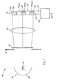
- the telecine projector 10 comprises a CCD sensor 12.
- the projector will comprise three sensors and means for splitting the projected light into its red, green and blue components and directing those components to respective sensors.
- the projector will comprise three sensors and means for splitting the projected light into its red, green and blue components and directing those components to respective sensors.
- a single sensor is shown in the drawings. This arrangement is suitable for use with black and white film.
- a further sensor is sometimes used, to which the infra red component of the light is directed. This is used to detect dust and scratches on the film, in a known manner.
- the sensor 12 comprises a line of photo-sensitive cells 14 1 , 14 2 ...14 n ...14 1440 .
- An image from a frame of film 16 may be projected onto the. sensor 12 by means of a light source and a lens system 22, both of which are shown schematically.
- a projected image generates a signal within each cell 14 representing the portion of the image falling on that cell.
- Control circuitry 24 sends signals controlling operation of the sensor 12 over the connection 25 and is operable to shift the generated signals along the line array towards an output port 26 provided at the end of the line of cells 14. The signals arrive at the output port 26 one after the other, and so may be read in serial form.
- Disconnecting means 28 is provided half way along the line between cells 14 720 and 14 721 and comprises an electronic switch which can connect the two halves of the line together to form a single line array sensor, or disconnect the two halves and discard signals from the half away from the output port 26 (cells 14 1 to 14 720 ) into a current sink, thereby forming a shorter line.
- the output port 26 is connected to the control circuitry 24 by a connection 27.
- the state of the electronic switch 28 is controlled by the control circuitry 24 over a connection 29, so that the circuitry can read signals from the whole of the line, or from the half adjacent the port 26 (cells 14721 to 14 1440 ) depending on the state of the switch 28.
- the structure of output ports for charge coupled devices is well known in the art.
- the film 16 for projection passes over a light gate 30 which is illuminated by the light source 20.
- the light source 20 is shown as comprising a bulb 32 and a reflector 34. In practice it will usually also include a condensor lens system. The detailed construction of a suitable light source form no part of the invention, and will be well understood by those skilled in the optics of telecine projectors.
- the lens system 22 is shown as a single bi-convex lens, but will usually be more complex in practice. Again, the details of construction of a suitable lens system form no part of the present invention, and are well known to those in the art.
- each signal is a packet of electrical charge whose size is proportional to the light intensity on the cell and to the exposure time.
- these signals are read by the control circuitry 24 by shifting them along the line of cells in a manner to be described in more detail later, to the output port 26.
- the circuitry 24 processes the signals which have been read, to generate a video signal representing the band of the image which gave rise to the signals.
- the resulting video signal is provided at an output terminal 36.
- the projector is shown in use, with anamorphic film 16 at the film gate 30.
- the anamorphism is indicated by an elliptical image 38 shown on the film and formed by a circular object, as discussed above.
- the line of photo-sensitive cells of the sensor 12 are located behind a window 40 in the device, : which is shown built into a standard DIL integrated circuit package. It is not necessary to correct the anamorphism of the film 16 during projection, because the image is sampled line by line, so that the vertical height of the image is not important.
- the magnification of the lens system 22 is adjusted so that the focused image falls on the sensor 12 along the whole length of the line of cells. Accordingly, the switch 28 connects the two halves of the line together and the port 26 (not shown in Figure 2) is used to' read from the whole length of the line.
- the data rate required in this case is 21.8 MHz, which is just acceptable with current CCD technology.
- the subsequent processing of the signals read from the cells is more complex when anamorphic film is being projected, than when normal or wide angle film is projected (to be described below) because only half of the image is used for the final television picture.
- half are discarded.
- the remainder (which may be signals from any 720 consecutive cells of the line) are used to generate a video signal.
- the selection is conveniently performed by loading all of the signals into a memory device, and then reading the selected 720 signals, as described below with reference to Figure 5.
- the control circuit changes the state of the switch 28 so that signals from the cells 141 to 14 720 are discarded into a current sink, and so that only signals from cells 14 721 to 14 1440 can be read through the port 26.
- image encoding may begin. Disconnecting half of the array halves the length of the line of cells for the purposes of clock frequency and data rate calculations, and reduces the required data rate to 18.97 MHz, (for wide angle film) or 13.9 MHz (for normal film) which are acceptable with current CCD technology.
- the aspect ratio of wide-angle film means that signals representing part of the width of the image must be discarded. The discard is performed in the same way as with anamorphic film, as will be described below.
- FIG 4 shows schematically the sensor 12 in more detail. Each cell is of the same construction, and so only one (14 1 ) need be described.
- the cell 14 comprises a photo-sensitive element 42 (a photodiode) and a storage element 44 which is part of a shift register.
- the storage elements of all the cells are shown in Figure 4 forming a single shift register, although preferably they form two registers as described above, each with its own output port, 26, the elements of alternate cells forming part of alternate shift registers.
- a single shift register is shown in Figure 4 for simplicity. Since the sensor 12 is a charge coupled device, the photo-sensitive element 42 and the storage element 44 are both sites in a semiconductor wafer.
- An electrode system 46 to which voltages are .applied by the circuitry 24, enables the circuitry 24 to control the transfer of a charge packet from the element 42 to the element 44.
- the action of the electrode system 46 is common to all of the cells 14, so that under the control of the circuitry 24, the signals generated by a projected image in the photo-sensitive elements of all of the cells 14 may be transferred simultaneously to the corresponding storage elements.
- the circuitry 24 also applies voltages to two further electrode systems 46,48. These voltages control the transfer of charge packets along the shift registers formed by the storage elements of the cells. Repeated application of the voltage patterns required to effect such transfer causes the signals stored in the storage elements of the cells to be shifted along the line of cells to the output port 26. Of course, the signals in the elements of the cells 1 4 1 to 14 720 may never reach the port 26, being discarded into a current sink by the switch 28.
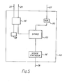
- Signals read from the output port 26 arrive over the connection 27 and are digitally encoded by an analogue-to- digital converter 60, before being stored in a store 62.
- Stored signals are read out of the store 62 under the control of circuit 64, and are fed to circuit 66 which generates a standard video signal from the stored signals.
- the video signal is provided at the output 36.
- the circuit 64 not only controls the reading of data from the store 62, but also controls the shifting of signals through the sensor, by means of the connection 25, and the state of the switch 28, by means of the connection 29.
- the circuit 64 sets the switch 28 to disconnect the two halves of the line of cells.
- Signals representing a line of the image arrive over the connection 27, and are stored as they arrive in the store 62 in place of the signals representing the previous image line (if any).
- the circuit 64 commands all 720 signals to be read out to the video signal.
- the circuit 64 controls data read-out so that not all of the stored signals are read out to the circuit 66.
- the selection has the effect of reducing the aspect ratio of the image (at the expense of losing part of its width) to the ratio required for display on a television . screen.
- a manually operable control 68 determines which signals are selected and, therefore, which part of the width of the image is selected for display. The control 68 enables the choice to change, as action moves across the frame, so that the final image can, in effect, pan across the full image on the film, to follow the action. .
- Selection is also performed when anamorphic film is being encoded.
- the two halves of the line of cells are connected, and 1440 signals arrive for each line of the image. These are all stored in the store 62.
- the circuit 64 controls data read-out so that only 720 consecutive signals are read from the store to the circuit 66, corresponding to the half of the image width which is to be displayed.
- the control 68 is again used to determine which signals are to be read out, so that the choice may be changed to pan the final image across the whole width of the anamorphic image to follow moving action.
- the sensor described above has 1440 elements, another number of elements could be chosen, according to factors such as the required resolution and the degree of anamorphism (the horizontal compression ratio) of the film being projected. Future developments in CCD technology, for instance any which increases the maximum acceptable clock rate, will also affect the choice of the number of elements chosen and the position of the switch 28 along the line of cells. Further switches like the switch 28 may be provided along the line of cells, to enable the line to have more than two effective lengths, if required by the range of film stock to be encoded.
- the invention is applicable not only to the CCDs of the type described above. Indeed the sensor need not necessarily be a charge coupled device.
- the problem addressed by the invention arises from the requirement that signals be read out of the sensor in serial form,, and the invention could also be applicable to other sensor systems in which the same requirement exists.
Landscapes
- Engineering & Computer Science (AREA)
- Multimedia (AREA)
- Signal Processing (AREA)
- Color Television Image Signal Generators (AREA)
- Facsimile Scanning Arrangements (AREA)
- Transforming Light Signals Into Electric Signals (AREA)
- Solid State Image Pick-Up Elements (AREA)
Applications Claiming Priority (2)
| Application Number | Priority Date | Filing Date | Title |
|---|---|---|---|
| GB8503169 | 1985-02-07 | ||
| GB08503169A GB2170974B (en) | 1985-02-07 | 1985-02-07 | Telecine projector line array sensor |
Publications (2)
| Publication Number | Publication Date |
|---|---|
| EP0193293A1 true EP0193293A1 (de) | 1986-09-03 |
| EP0193293B1 EP0193293B1 (de) | 1989-06-07 |
Family
ID=10574113
Family Applications (1)
| Application Number | Title | Priority Date | Filing Date |
|---|---|---|---|
| EP86300760A Expired EP0193293B1 (de) | 1985-02-07 | 1986-02-05 | Zeilensensor für Fernsehfilmprojektoren |
Country Status (5)
| Country | Link |
|---|---|
| US (1) | US4703365A (de) |
| EP (1) | EP0193293B1 (de) |
| JP (1) | JPS61245676A (de) |
| DE (1) | DE3663874D1 (de) |
| GB (1) | GB2170974B (de) |
Families Citing this family (12)
| Publication number | Priority date | Publication date | Assignee | Title |
|---|---|---|---|---|
| JP2623530B2 (ja) * | 1986-04-22 | 1997-06-25 | ミノルタ株式会社 | 固体撮像素子駆動装置 |
| DE3887547T2 (de) * | 1987-03-20 | 1994-08-25 | Canon Kk | Abbildungsgerät. |
| JPS63245073A (ja) * | 1987-03-31 | 1988-10-12 | Canon Inc | 撮像装置 |
| US4959736A (en) * | 1987-12-29 | 1990-09-25 | Minolta Camera Kabushiki Kaisha | Image signal processing method and apparatus with elongated picture elements |
| JPH01311775A (ja) * | 1988-06-10 | 1989-12-15 | Asahi Optical Co Ltd | Ccdセンサの駆動方法 |
| US5045932A (en) * | 1989-06-29 | 1991-09-03 | Eastman Kodak Company | Method and apparatus for generating a high definition electronic signal from a line scan of a color original |
| JPH03250856A (ja) * | 1990-02-28 | 1991-11-08 | Sharp Corp | 固体撮像素子の読み出し回路 |
| US5680172A (en) * | 1992-01-21 | 1997-10-21 | Video Post & Transfer, Inc. | Consecutive frame scanning of cinematographic film |
| JP3487361B2 (ja) * | 1994-04-11 | 2004-01-19 | 富士写真フイルム株式会社 | フイルムスキャナの露出制御装置並びに画像信号処理方法及びガンマ補正方法 |
| US6614471B1 (en) | 1999-05-10 | 2003-09-02 | Banctec, Inc. | Luminance correction for color scanning using a measured and derived luminance value |
| TW462180B (en) * | 2000-03-29 | 2001-11-01 | Avision Inc | CCD image sensor device and method to sense image quickly |
| DE10115342A1 (de) * | 2001-03-28 | 2002-10-02 | Philips Corp Intellectual Pty | Einrichtung zum Abtasten von Filmen |
Citations (3)
| Publication number | Priority date | Publication date | Assignee | Title |
|---|---|---|---|---|
| GB2007935A (en) * | 1977-11-14 | 1979-05-23 | British Broadcasting Corp | Telecine machine |
| US4205337A (en) * | 1977-07-06 | 1980-05-27 | The Rank Organisation Limited | Television film scanner |
| US4476493A (en) * | 1981-04-16 | 1984-10-09 | Robert Bosch Gmbh | Television scanning of motion picture films of different frame aspect ratios |
Family Cites Families (3)
| Publication number | Priority date | Publication date | Assignee | Title |
|---|---|---|---|---|
| US4249217A (en) * | 1979-05-29 | 1981-02-03 | International Business Machines Corporation | Separated sensor array abutment |
| JPS57121368A (en) * | 1981-01-22 | 1982-07-28 | Canon Inc | Method for picture scanning |
| JPS57178479A (en) * | 1981-04-27 | 1982-11-02 | Sony Corp | Solid image pickup element |
-
1985
- 1985-02-07 GB GB08503169A patent/GB2170974B/en not_active Expired
-
1986
- 1986-01-30 US US06/824,183 patent/US4703365A/en not_active Expired - Lifetime
- 1986-02-05 DE DE8686300760T patent/DE3663874D1/de not_active Expired
- 1986-02-05 EP EP86300760A patent/EP0193293B1/de not_active Expired
- 1986-02-07 JP JP61024253A patent/JPS61245676A/ja active Pending
Patent Citations (3)
| Publication number | Priority date | Publication date | Assignee | Title |
|---|---|---|---|---|
| US4205337A (en) * | 1977-07-06 | 1980-05-27 | The Rank Organisation Limited | Television film scanner |
| GB2007935A (en) * | 1977-11-14 | 1979-05-23 | British Broadcasting Corp | Telecine machine |
| US4476493A (en) * | 1981-04-16 | 1984-10-09 | Robert Bosch Gmbh | Television scanning of motion picture films of different frame aspect ratios |
Non-Patent Citations (1)
| Title |
|---|
| RUNDFUNKTECHNISCHE MITTEILUNGEN, vol. 28, no. 1, 1984, Hamburg DIETER POETSCH 'FDLGO-Ein System zur fortschrittlichen Filmabtastung" pages 10-22 * |
Also Published As
| Publication number | Publication date |
|---|---|
| DE3663874D1 (en) | 1989-07-13 |
| US4703365A (en) | 1987-10-27 |
| GB2170974A (en) | 1986-08-13 |
| EP0193293B1 (de) | 1989-06-07 |
| GB8503169D0 (en) | 1985-03-13 |
| GB2170974B (en) | 1988-01-06 |
| JPS61245676A (ja) | 1986-10-31 |
Similar Documents
| Publication | Publication Date | Title |
|---|---|---|
| US7113213B2 (en) | Image system, solid-state imaging semiconductor integrated circuit device used in the image system, and difference output method used for the image system | |
| US6674470B1 (en) | MOS-type solid state imaging device with high sensitivity | |
| US6831692B1 (en) | Solid-state image pickup apparatus capable of outputting high definition image signals with photosensitive cells different in sensitivity and signal reading method | |
| US4603354A (en) | Image pickup device | |
| EP0193293B1 (de) | Zeilensensor für Fernsehfilmprojektoren | |
| JPH0318393B2 (de) | ||
| US4331979A (en) | Line-scan still image reproducer | |
| JP3461265B2 (ja) | 固体撮像装置および固体撮像装置応用システム | |
| US4179711A (en) | Defect noise compensating system | |
| US5216511A (en) | Imaging device with elimination of dark current | |
| US3803353A (en) | Optical-to-electrical signal transducer method and apparatus | |
| US5877807A (en) | Optoelectronic colored image converter | |
| JPH10308507A (ja) | 固体撮像装置および固体撮像装置応用システム | |
| US6687026B1 (en) | Optical scanning apparatus with switchable resolution | |
| US5737098A (en) | Electronic color snapshot technique and structure using very high resolution monochrome full frame CCD imagers | |
| US5081525A (en) | Opto-electric converting image pickup element and image pickup apparatus employing the same | |
| JPS6211264A (ja) | 固体撮像装置 | |
| JPH10189930A (ja) | 固体撮像素子 | |
| JPH0233273A (ja) | 撮像装置 | |
| JPS5815372A (ja) | 固体テレビカメラ装置 | |
| JPS61121577A (ja) | 撮像装置 | |
| JPS6247278A (ja) | 電子カメラ | |
| EP0238111B1 (de) | Kamera zur Aufnahme von Fernsehbildern, photographischen oder kinematographischen Bildern mit automatischer Fokussierungsvorrichtung | |
| KR20010070240A (ko) | 능동 픽셀 센서 및 능동 픽셀 센서 회로 | |
| Poetsch | A continuous-motion color film telecine using CCD line sensors |
Legal Events
| Date | Code | Title | Description |
|---|---|---|---|
| PUAI | Public reference made under article 153(3) epc to a published international application that has entered the european phase |
Free format text: ORIGINAL CODE: 0009012 |
|
| AK | Designated contracting states |
Kind code of ref document: A1 Designated state(s): DE FR NL |
|
| 17P | Request for examination filed |
Effective date: 19861211 |
|
| 17Q | First examination report despatched |
Effective date: 19881102 |
|
| GRAA | (expected) grant |
Free format text: ORIGINAL CODE: 0009210 |
|
| AK | Designated contracting states |
Kind code of ref document: B1 Designated state(s): DE FR NL |
|
| REF | Corresponds to: |
Ref document number: 3663874 Country of ref document: DE Date of ref document: 19890713 |
|
| ET | Fr: translation filed | ||
| PLBI | Opposition filed |
Free format text: ORIGINAL CODE: 0009260 |
|
| 26 | Opposition filed |
Opponent name: BTS BROADCAST TELEVISION SYSTEMS GMBH Effective date: 19900306 |
|
| NLR1 | Nl: opposition has been filed with the epo |
Opponent name: BTS BROADCAST TELEVISION SYSTEMS GMBH |
|
| PLBN | Opposition rejected |
Free format text: ORIGINAL CODE: 0009273 |
|
| STAA | Information on the status of an ep patent application or granted ep patent |
Free format text: STATUS: OPPOSITION REJECTED |
|
| 27O | Opposition rejected |
Effective date: 19910422 |
|
| NLR2 | Nl: decision of opposition | ||
| REG | Reference to a national code |
Ref country code: FR Ref legal event code: TP |
|
| NLS | Nl: assignments of ep-patents |
Owner name: CINTEL INTERNATIONAL LIMITED |
|
| PGFP | Annual fee paid to national office [announced via postgrant information from national office to epo] |
Ref country code: DE Payment date: 19991231 Year of fee payment: 15 |
|
| PGFP | Annual fee paid to national office [announced via postgrant information from national office to epo] |
Ref country code: FR Payment date: 20000210 Year of fee payment: 15 |
|
| PGFP | Annual fee paid to national office [announced via postgrant information from national office to epo] |
Ref country code: NL Payment date: 20000228 Year of fee payment: 15 |
|
| PG25 | Lapsed in a contracting state [announced via postgrant information from national office to epo] |
Ref country code: NL Free format text: LAPSE BECAUSE OF NON-PAYMENT OF DUE FEES Effective date: 20010901 |
|
| PG25 | Lapsed in a contracting state [announced via postgrant information from national office to epo] |
Ref country code: FR Free format text: LAPSE BECAUSE OF NON-PAYMENT OF DUE FEES Effective date: 20011031 |
|
| NLV4 | Nl: lapsed or anulled due to non-payment of the annual fee |
Effective date: 20010901 |
|
| REG | Reference to a national code |
Ref country code: FR Ref legal event code: ST |
|
| PG25 | Lapsed in a contracting state [announced via postgrant information from national office to epo] |
Ref country code: DE Free format text: LAPSE BECAUSE OF NON-PAYMENT OF DUE FEES Effective date: 20011201 |