EP0190657A2 - Guide optique de verre de silice - Google Patents
Guide optique de verre de silice Download PDFInfo
- Publication number
- EP0190657A2 EP0190657A2 EP86101161A EP86101161A EP0190657A2 EP 0190657 A2 EP0190657 A2 EP 0190657A2 EP 86101161 A EP86101161 A EP 86101161A EP 86101161 A EP86101161 A EP 86101161A EP 0190657 A2 EP0190657 A2 EP 0190657A2
- Authority
- EP
- European Patent Office
- Prior art keywords
- silica glass
- varnish
- optical conductor
- ppm
- glass optical
- Prior art date
- Legal status (The legal status is an assumption and is not a legal conclusion. Google has not performed a legal analysis and makes no representation as to the accuracy of the status listed.)
- Granted
Links
- VYPSYNLAJGMNEJ-UHFFFAOYSA-N Silicium dioxide Chemical compound O=[Si]=O VYPSYNLAJGMNEJ-UHFFFAOYSA-N 0.000 title claims abstract description 29
- 230000003287 optical effect Effects 0.000 title claims description 27
- 239000004020 conductor Substances 0.000 title claims description 24
- 239000013307 optical fiber Substances 0.000 claims abstract description 22
- 239000004642 Polyimide Substances 0.000 claims abstract description 20
- 229920001721 polyimide Polymers 0.000 claims abstract description 20
- DGAQECJNVWCQMB-PUAWFVPOSA-M Ilexoside XXIX Chemical compound C[C@@H]1CC[C@@]2(CC[C@@]3(C(=CC[C@H]4[C@]3(CC[C@@H]5[C@@]4(CC[C@@H](C5(C)C)OS(=O)(=O)[O-])C)C)[C@@H]2[C@]1(C)O)C)C(=O)O[C@H]6[C@@H]([C@H]([C@@H]([C@H](O6)CO)O)O)O.[Na+] DGAQECJNVWCQMB-PUAWFVPOSA-M 0.000 claims abstract description 15
- ZLMJMSJWJFRBEC-UHFFFAOYSA-N Potassium Chemical compound [K] ZLMJMSJWJFRBEC-UHFFFAOYSA-N 0.000 claims abstract description 15
- 229910052700 potassium Inorganic materials 0.000 claims abstract description 15
- 239000011591 potassium Substances 0.000 claims abstract description 15
- 229910052708 sodium Inorganic materials 0.000 claims abstract description 15
- 239000011734 sodium Substances 0.000 claims abstract description 15
- 239000011247 coating layer Substances 0.000 claims abstract description 6
- 238000005286 illumination Methods 0.000 claims description 4
- 230000005855 radiation Effects 0.000 abstract description 12
- 239000010410 layer Substances 0.000 description 24
- 239000002966 varnish Substances 0.000 description 13
- 230000000052 comparative effect Effects 0.000 description 10
- GTDPSWPPOUPBNX-UHFFFAOYSA-N ac1mqpva Chemical compound CC12C(=O)OC(=O)C1(C)C1(C)C2(C)C(=O)OC1=O GTDPSWPPOUPBNX-UHFFFAOYSA-N 0.000 description 7
- 238000005253 cladding Methods 0.000 description 7
- 125000005462 imide group Chemical group 0.000 description 5
- 239000000835 fiber Substances 0.000 description 4
- 238000007670 refining Methods 0.000 description 4
- 235000012239 silicon dioxide Nutrition 0.000 description 4
- UHOVQNZJYSORNB-UHFFFAOYSA-N Benzene Chemical compound C1=CC=CC=C1 UHOVQNZJYSORNB-UHFFFAOYSA-N 0.000 description 3
- YXFVVABEGXRONW-UHFFFAOYSA-N Toluene Chemical compound CC1=CC=CC=C1 YXFVVABEGXRONW-UHFFFAOYSA-N 0.000 description 3
- 238000010438 heat treatment Methods 0.000 description 3
- 239000000463 material Substances 0.000 description 3
- 239000000203 mixture Substances 0.000 description 3
- ZOXJGFHDIHLPTG-UHFFFAOYSA-N Boron Chemical compound [B] ZOXJGFHDIHLPTG-UHFFFAOYSA-N 0.000 description 2
- RTZKZFJDLAIYFH-UHFFFAOYSA-N Diethyl ether Chemical compound CCOCC RTZKZFJDLAIYFH-UHFFFAOYSA-N 0.000 description 2
- PXGOKWXKJXAPGV-UHFFFAOYSA-N Fluorine Chemical compound FF PXGOKWXKJXAPGV-UHFFFAOYSA-N 0.000 description 2
- 235000002918 Fraxinus excelsior Nutrition 0.000 description 2
- 239000004952 Polyamide Substances 0.000 description 2
- 239000002956 ash Substances 0.000 description 2
- 229910052796 boron Inorganic materials 0.000 description 2
- 239000011248 coating agent Substances 0.000 description 2
- 238000000576 coating method Methods 0.000 description 2
- 150000004985 diamines Chemical class 0.000 description 2
- 125000005442 diisocyanate group Chemical group 0.000 description 2
- 229910052731 fluorine Inorganic materials 0.000 description 2
- 239000011737 fluorine Substances 0.000 description 2
- BASFCYQUMIYNBI-UHFFFAOYSA-N platinum Chemical compound [Pt] BASFCYQUMIYNBI-UHFFFAOYSA-N 0.000 description 2
- 229920002647 polyamide Polymers 0.000 description 2
- BITYAPCSNKJESK-UHFFFAOYSA-N potassiosodium Chemical compound [Na].[K] BITYAPCSNKJESK-UHFFFAOYSA-N 0.000 description 2
- 150000000000 tetracarboxylic acids Chemical class 0.000 description 2
- ZTNJGMFHJYGMDR-UHFFFAOYSA-N 1,2-diisocyanatoethane Chemical compound O=C=NCCN=C=O ZTNJGMFHJYGMDR-UHFFFAOYSA-N 0.000 description 1
- WZCQRUWWHSTZEM-UHFFFAOYSA-N 1,3-phenylenediamine Chemical compound NC1=CC=CC(N)=C1 WZCQRUWWHSTZEM-UHFFFAOYSA-N 0.000 description 1
- ALQLPWJFHRMHIU-UHFFFAOYSA-N 1,4-diisocyanatobenzene Chemical compound O=C=NC1=CC=C(N=C=O)C=C1 ALQLPWJFHRMHIU-UHFFFAOYSA-N 0.000 description 1
- CBCKQZAAMUWICA-UHFFFAOYSA-N 1,4-phenylenediamine Chemical compound NC1=CC=C(N)C=C1 CBCKQZAAMUWICA-UHFFFAOYSA-N 0.000 description 1
- 229940008841 1,6-hexamethylene diisocyanate Drugs 0.000 description 1
- VLDPXPPHXDGHEW-UHFFFAOYSA-N 1-chloro-2-dichlorophosphoryloxybenzene Chemical compound ClC1=CC=CC=C1OP(Cl)(Cl)=O VLDPXPPHXDGHEW-UHFFFAOYSA-N 0.000 description 1
- XMXCPDQUXVZBGQ-UHFFFAOYSA-N 2,3,6,7-tetrachloronaphthalene-1,4,5,8-tetracarboxylic acid Chemical compound ClC1=C(Cl)C(C(O)=O)=C2C(C(=O)O)=C(Cl)C(Cl)=C(C(O)=O)C2=C1C(O)=O XMXCPDQUXVZBGQ-UHFFFAOYSA-N 0.000 description 1
- SDWGBHZZXPDKDZ-UHFFFAOYSA-N 2,6-dichloronaphthalene-1,4,5,8-tetracarboxylic acid Chemical compound C1=C(Cl)C(C(O)=O)=C2C(C(=O)O)=CC(Cl)=C(C(O)=O)C2=C1C(O)=O SDWGBHZZXPDKDZ-UHFFFAOYSA-N 0.000 description 1
- HUWXDEQWWKGHRV-UHFFFAOYSA-N 3,3'-Dichlorobenzidine Chemical compound C1=C(Cl)C(N)=CC=C1C1=CC=C(N)C(Cl)=C1 HUWXDEQWWKGHRV-UHFFFAOYSA-N 0.000 description 1
- JRBJSXQPQWSCCF-UHFFFAOYSA-N 3,3'-Dimethoxybenzidine Chemical compound C1=C(N)C(OC)=CC(C=2C=C(OC)C(N)=CC=2)=C1 JRBJSXQPQWSCCF-UHFFFAOYSA-N 0.000 description 1
- NUIURNJTPRWVAP-UHFFFAOYSA-N 3,3'-Dimethylbenzidine Chemical group C1=C(N)C(C)=CC(C=2C=C(C)C(N)=CC=2)=C1 NUIURNJTPRWVAP-UHFFFAOYSA-N 0.000 description 1
- LJGHYPLBDBRCRZ-UHFFFAOYSA-N 3-(3-aminophenyl)sulfonylaniline Chemical compound NC1=CC=CC(S(=O)(=O)C=2C=C(N)C=CC=2)=C1 LJGHYPLBDBRCRZ-UHFFFAOYSA-N 0.000 description 1
- ICNFHJVPAJKPHW-UHFFFAOYSA-N 4,4'-Thiodianiline Chemical compound C1=CC(N)=CC=C1SC1=CC=C(N)C=C1 ICNFHJVPAJKPHW-UHFFFAOYSA-N 0.000 description 1
- YBRVSVVVWCFQMG-UHFFFAOYSA-N 4,4'-diaminodiphenylmethane Chemical compound C1=CC(N)=CC=C1CC1=CC=C(N)C=C1 YBRVSVVVWCFQMG-UHFFFAOYSA-N 0.000 description 1
- HLBLWEWZXPIGSM-UHFFFAOYSA-N 4-Aminophenyl ether Chemical compound C1=CC(N)=CC=C1OC1=CC=C(N)C=C1 HLBLWEWZXPIGSM-UHFFFAOYSA-N 0.000 description 1
- OSGFBINRYVUILV-UHFFFAOYSA-N 4-[(4-aminophenyl)-diethylsilyl]aniline Chemical compound C=1C=C(N)C=CC=1[Si](CC)(CC)C1=CC=C(N)C=C1 OSGFBINRYVUILV-UHFFFAOYSA-N 0.000 description 1
- BLMSGSGJGUHKFW-UHFFFAOYSA-N 4-[(4-aminophenyl)-diphenylsilyl]aniline Chemical compound C1=CC(N)=CC=C1[Si](C=1C=CC(N)=CC=1)(C=1C=CC=CC=1)C1=CC=CC=C1 BLMSGSGJGUHKFW-UHFFFAOYSA-N 0.000 description 1
- KTZLSMUPEJXXBO-UHFFFAOYSA-N 4-[(4-aminophenyl)-phenylphosphoryl]aniline Chemical compound C1=CC(N)=CC=C1P(=O)(C=1C=CC(N)=CC=1)C1=CC=CC=C1 KTZLSMUPEJXXBO-UHFFFAOYSA-N 0.000 description 1
- ZYEDGEXYGKWJPB-UHFFFAOYSA-N 4-[2-(4-aminophenyl)propan-2-yl]aniline Chemical compound C=1C=C(N)C=CC=1C(C)(C)C1=CC=C(N)C=C1 ZYEDGEXYGKWJPB-UHFFFAOYSA-N 0.000 description 1
- HWKHQQCBFMYAJZ-UHFFFAOYSA-N 4-amino-n-(3-aminophenyl)benzamide Chemical compound C1=CC(N)=CC=C1C(=O)NC1=CC=CC(N)=C1 HWKHQQCBFMYAJZ-UHFFFAOYSA-N 0.000 description 1
- VMFQOYLCRZRUMB-UHFFFAOYSA-N 4-n-(4-aminophenyl)-4-n-butylbenzene-1,4-diamine Chemical compound C=1C=C(N)C=CC=1N(CCCC)C1=CC=C(N)C=C1 VMFQOYLCRZRUMB-UHFFFAOYSA-N 0.000 description 1
- LBNFPUAJWZYIOQ-UHFFFAOYSA-N 4-n-(4-aminophenyl)-4-n-methylbenzene-1,4-diamine Chemical compound C=1C=C(N)C=CC=1N(C)C1=CC=C(N)C=C1 LBNFPUAJWZYIOQ-UHFFFAOYSA-N 0.000 description 1
- YFBMJEBQWQBRQJ-UHFFFAOYSA-N 4-n-(4-aminophenyl)-4-n-phenylbenzene-1,4-diamine Chemical compound C1=CC(N)=CC=C1N(C=1C=CC(N)=CC=1)C1=CC=CC=C1 YFBMJEBQWQBRQJ-UHFFFAOYSA-N 0.000 description 1
- IIEKUGPEYLGWQQ-UHFFFAOYSA-N 5-[4-(4-amino-2-methylpentyl)phenyl]-4-methylpentan-2-amine Chemical compound CC(N)CC(C)CC1=CC=C(CC(C)CC(C)N)C=C1 IIEKUGPEYLGWQQ-UHFFFAOYSA-N 0.000 description 1
- OKTJSMMVPCPJKN-UHFFFAOYSA-N Carbon Chemical compound [C] OKTJSMMVPCPJKN-UHFFFAOYSA-N 0.000 description 1
- MQJKPEGWNLWLTK-UHFFFAOYSA-N Dapsone Chemical compound C1=CC(N)=CC=C1S(=O)(=O)C1=CC=C(N)C=C1 MQJKPEGWNLWLTK-UHFFFAOYSA-N 0.000 description 1
- HNQHUWHQMJTWRA-UHFFFAOYSA-N NC1=CC=C(C=C1)C(C[PH2]=O)C1=CC=C(C=C1)N Chemical compound NC1=CC=C(C=C1)C(C[PH2]=O)C1=CC=C(C=C1)N HNQHUWHQMJTWRA-UHFFFAOYSA-N 0.000 description 1
- 239000004962 Polyamide-imide Substances 0.000 description 1
- FDLQZKYLHJJBHD-UHFFFAOYSA-N [3-(aminomethyl)phenyl]methanamine Chemical compound NCC1=CC=CC(CN)=C1 FDLQZKYLHJJBHD-UHFFFAOYSA-N 0.000 description 1
- ISKQADXMHQSTHK-UHFFFAOYSA-N [4-(aminomethyl)phenyl]methanamine Chemical compound NCC1=CC=C(CN)C=C1 ISKQADXMHQSTHK-UHFFFAOYSA-N 0.000 description 1
- 238000010521 absorption reaction Methods 0.000 description 1
- 239000002253 acid Substances 0.000 description 1
- 125000002723 alicyclic group Chemical group 0.000 description 1
- 125000001931 aliphatic group Chemical group 0.000 description 1
- 239000007864 aqueous solution Substances 0.000 description 1
- 125000003118 aryl group Chemical group 0.000 description 1
- HFACYLZERDEVSX-UHFFFAOYSA-N benzidine Chemical compound C1=CC(N)=CC=C1C1=CC=C(N)C=C1 HFACYLZERDEVSX-UHFFFAOYSA-N 0.000 description 1
- ZLSMCQSGRWNEGX-UHFFFAOYSA-N bis(4-aminophenyl)methanone Chemical compound C1=CC(N)=CC=C1C(=O)C1=CC=C(N)C=C1 ZLSMCQSGRWNEGX-UHFFFAOYSA-N 0.000 description 1
- 229910052799 carbon Inorganic materials 0.000 description 1
- 239000002019 doping agent Substances 0.000 description 1
- 239000011521 glass Substances 0.000 description 1
- 125000000623 heterocyclic group Chemical group 0.000 description 1
- RRAMGCGOFNQTLD-UHFFFAOYSA-N hexamethylene diisocyanate Chemical compound O=C=NCCCCCCN=C=O RRAMGCGOFNQTLD-UHFFFAOYSA-N 0.000 description 1
- 238000005259 measurement Methods 0.000 description 1
- 238000000034 method Methods 0.000 description 1
- KADGVXXDDWDKBX-UHFFFAOYSA-N naphthalene-1,2,4,5-tetracarboxylic acid Chemical compound OC(=O)C1=CC=CC2=C(C(O)=O)C(C(=O)O)=CC(C(O)=O)=C21 KADGVXXDDWDKBX-UHFFFAOYSA-N 0.000 description 1
- OBKARQMATMRWQZ-UHFFFAOYSA-N naphthalene-1,2,5,6-tetracarboxylic acid Chemical compound OC(=O)C1=C(C(O)=O)C=CC2=C(C(O)=O)C(C(=O)O)=CC=C21 OBKARQMATMRWQZ-UHFFFAOYSA-N 0.000 description 1
- KQSABULTKYLFEV-UHFFFAOYSA-N naphthalene-1,5-diamine Chemical compound C1=CC=C2C(N)=CC=CC2=C1N KQSABULTKYLFEV-UHFFFAOYSA-N 0.000 description 1
- DOBFTMLCEYUAQC-UHFFFAOYSA-N naphthalene-2,3,6,7-tetracarboxylic acid Chemical compound OC(=O)C1=C(C(O)=O)C=C2C=C(C(O)=O)C(C(=O)O)=CC2=C1 DOBFTMLCEYUAQC-UHFFFAOYSA-N 0.000 description 1
- YTVNOVQHSGMMOV-UHFFFAOYSA-N naphthalenetetracarboxylic dianhydride Chemical compound C1=CC(C(=O)OC2=O)=C3C2=CC=C2C(=O)OC(=O)C1=C32 YTVNOVQHSGMMOV-UHFFFAOYSA-N 0.000 description 1
- 125000000962 organic group Chemical group 0.000 description 1
- 229920000620 organic polymer Polymers 0.000 description 1
- JGGWKXMPICYBKC-UHFFFAOYSA-N phenanthrene-1,8,9,10-tetracarboxylic acid Chemical compound C1=CC=C(C(O)=O)C2=C(C(O)=O)C(C(O)=O)=C3C(C(=O)O)=CC=CC3=C21 JGGWKXMPICYBKC-UHFFFAOYSA-N 0.000 description 1
- CLYVDMAATCIVBF-UHFFFAOYSA-N pigment red 224 Chemical compound C=12C3=CC=C(C(OC4=O)=O)C2=C4C=CC=1C1=CC=C2C(=O)OC(=O)C4=CC=C3C1=C42 CLYVDMAATCIVBF-UHFFFAOYSA-N 0.000 description 1
- 229910052697 platinum Inorganic materials 0.000 description 1
- 229920002312 polyamide-imide Polymers 0.000 description 1
- VHNQIURBCCNWDN-UHFFFAOYSA-N pyridine-2,6-diamine Chemical compound NC1=CC=CC(N)=N1 VHNQIURBCCNWDN-UHFFFAOYSA-N 0.000 description 1
- 230000002285 radioactive effect Effects 0.000 description 1
- 239000002994 raw material Substances 0.000 description 1
- 239000000377 silicon dioxide Substances 0.000 description 1
- 239000002904 solvent Substances 0.000 description 1
- LUEGQDUCMILDOJ-UHFFFAOYSA-N thiophene-2,3,4,5-tetracarboxylic acid Chemical compound OC(=O)C=1SC(C(O)=O)=C(C(O)=O)C=1C(O)=O LUEGQDUCMILDOJ-UHFFFAOYSA-N 0.000 description 1
- RUELTTOHQODFPA-UHFFFAOYSA-N toluene 2,6-diisocyanate Chemical compound CC1=C(N=C=O)C=CC=C1N=C=O RUELTTOHQODFPA-UHFFFAOYSA-N 0.000 description 1
Images
Classifications
-
- G—PHYSICS
- G02—OPTICS
- G02B—OPTICAL ELEMENTS, SYSTEMS OR APPARATUS
- G02B6/00—Light guides; Structural details of arrangements comprising light guides and other optical elements, e.g. couplings
- G02B6/04—Light guides; Structural details of arrangements comprising light guides and other optical elements, e.g. couplings formed by bundles of fibres
- G02B6/06—Light guides; Structural details of arrangements comprising light guides and other optical elements, e.g. couplings formed by bundles of fibres the relative position of the fibres being the same at both ends, e.g. for transporting images
Definitions
- the present invention relates to a silica gleN eptieal conductor, such as an optical fiber for telecommunication, a multiple fiber for an image scope, and a light guide for illumination.
- a silica gleN eptieal conductor such as an optical fiber for telecommunication, a multiple fiber for an image scope, and a light guide for illumination.
- silica glass optical conductors which are prepared by drawing their preforms and applying a primary coating layer ( hereinafter the term, primary coating layer being briefly referred to as precoating layer ) on the surface thereof, have excellent radiation resistance as compared with multi-component glass optical conductors and, therefore, is suitable to be used in nuclear facilities. According to the studies of the present inventors, however, the radiation resistance of the silica glass optical conductors are various, and are varied by the material of the precoating layer.
- An object of the present invention is to provide a radiation and heat resistant silica glass optical conductor.
- Another object of the present invention is to provide a radiation and heat resistant optical fiber used for telecommunication.
- Still another object of the present invention is to provide a radiation and heat resistant multiple optical fiber used for various industrial facilities, meducal equipments and nuclear facilities.
- Still another object of the present invention is to provide a radiation and heat resistant light guide used for illumination.
- the present invention provides a silica glass optical conductor having a precoating layer composed of a polyimide whose total content of sodium element and potassium element is less than 50 ppm.
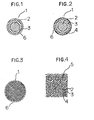
- FIG. 1 and 2 are cross-sectional views of an optical fiber for telecommunication or a light guide for illumination in accordance with the present invention.
- Fig. 3 is a cross-sectional view of a multiple optical fiber in accordance with the present invention.
- Fig.4 is a magnified view of Fig. 3 in a portion of the cross-section.
- each optical conductor 1 comprises a core 2 and a cladding layer 3.
- the optical conductor 1 shown in Fig. 2 has furthermore a supporting layer 4 formed on the cladding layer 3.
- the optical conductore 1 shown in Fig. 3, which is a multiple optical conductor, has such a structure that a plurality of unit optical conductors 5 each of which consists of a core 2, a cladding layer 3 and a supporting layer 4 are fused together.
- Each of the optical conductores of Figs. 1 to 3 has a precoating layer 6 on the cladding layer 3 or on the supporting layer 4.
- the core 2, the cladding layer 3 and the supporting layer 4 is composed of a natural or synthetic silica glass doped with or without a dopant, respectively.
- the core 2 is composed of a pure silica glass having a purity of at least 99.99 % by weight
- the cladding layer 3 is composed of a pure silica glass doped with boron and / or fluorine
- the supporting layer 4 is composed of a pure silica glass having a purity of at least 99.9 % by weight.
- Preferable polyimides to be used in the present invention are less than 10 ppm, especially less than 5 ppm in the total content of sodium element and potassium element, becauce the lower the above total content is,the more excellent in radiation resistance of the silica glass optical conductor.
- a great variety of organic polymer having an imide group in main chain thereof may be used as polyimide in the present invention so far as it satisfies the requirement concerning the sodium-potassium content mentioned above.
- such a polyimide is preferably used, which is at least 30 mole % , more preferably at least 50 mole % in the content of the recurring imide group represented by the following formula (1):
- the recurring imide group is defined as the same recurring imide group of a polyimide which is prepared by reacting a diamine or a diisocyanate with a tetracarboxylic acid or a derivative thereof and thenafter by heating the polyamide acid thus obtained in order to change it to the polyimide, and the R,,R 2 in the formula (1) are tetra-valent organic group of aliphatic, alicyclic, aromatic,or heterocyclic nature having a total carbon number of from about 4 to about 50, especially from about 6 to about 20, decided by the reacting raw materials used.
- diamine examples include meta-phenylene diamine; para- phenylene diamine; 2,2-bis(4-amino p henyl)propane; 4,4'-diaminodiphenyl methane; 4,4'-diaminodiphenyl sulfide; 4,4'-diaminodiphenyl sulfone; 3,3'-diaminodiphenyl sulfone; 4,4'-diaminodiphenyl ether; 2,6-diaminopyridine; bis(4-aminophenyl)diethyl silane; bis(4-aminophenyl)diphenyl silane; benzidine; 3,3'-dichlorobenzidine; 3,3'-dimethoxybenzidine; bis(4-aminophenyl)ethyl phosphine oxide; 4,4'-diaminobenzophenone; bis(4-aminophenyl)pheny
- diisocyanate examples include ethylene diisocyanate; 1,4-tetramethylene diisocyanate; 1,6-hexamethylene diisocyanate; 1,12-dodecane diisocyanate; cyclobutene-1,3-diisocyanate; cyclohexane-1,3 and-1,4-diisocyanate; 1,3- and 1,4-phenylene diisocyanate; 2,4-and 2,6-tolylene diisocyanate; and mixtures thereof.
- tetra-carboxylic acid or derivatives thereof are pyromellitic dianhydride; 2,3,6.7-naphthalenetetracarboxylic dianhydride; 1,2,5,6-naphthalene-tetra- carboxylic anhydride; 3,4,9,10-perylene tetracarboxylic dianhydride; naphthalene-1,2,4,5-tetracarboxylic dianhydride; naphthalene-1,4,5,8-tetracarboxylic dianhydride; 2,6-di- chloronaphthalene-1,4,5,8-tetracarboxylic dianhydride; 2,7-dichIoronaphghalene-1,4,5,8-tetracarboxylic dianhydride; 2,3,6,7-tetrachloronaphthalene-1,4,5,8-tetracarboxylic dianhydride; phenanthrene-1,8,9.10-tetracarboxylic dianhydr
- polyamides useful in the present invention are conventional polyimides,that is those substantially 100 mol % in the amount of imide group represented
- the precoating layer 6 can be formed easily by coating on the surface of a naked silica glass optical conductor with for example, a commercially available polyimide varnish which satisfies the above mentioned requirement concerning sodium-potassium content, and then by baking the varnish layer.
- the coating of the varnish is conducted preferably as soon as the naked silica glass optical conductor is just formed by heat-drawing a preform thereof.
- the thickness of the precoating layer 6 is preferably at least 5,um from a standpoint of obtaining a silica glass optical conductor having more excellent radiation resistance , furtheremore at least 10 ⁇ m, especially in the case of obtaining a silica glass multiple optical fiber.
- the optical fibers each of which has a three-layer structure consisting of a pure silica glass core, a cladding layer composed of a silica glass doped with boron and fluorine, and a support layer composed of a natural silica glass, were filled compactly in a natural silica glass tube. and then the tube was drawn by heating to a temperature of 2,100 °C to form a multiple optical fiber having an outer diameter of 1.0 mm.
- the multiple optical fiber was coated with a polyimide varnish ( hereinafter referred to as Varnish A ) of Du.Pont Co. ( U.S.A.) 65 ppm in potassium content,and 19 ppm in sodium content, and baked to form a baked polyimide precoating layer 50 ⁇ m in thickness on the surface of the multiple optical fiber.
- Varnish A of Du.Pont Co.
- a multiple optical fiber was produced in the same manner as in Comparative Example 1 except that a polyimide varnish ( Varnish B ) of Tore Co. ( Japan ) 80 ppm in potassium content and 20 ppm in sodium content was used instead of Varnish A.
- a polyimide varnish ( Varnish B ) of Tore Co. ( Japan ) 80 ppm in potassium content and 20 ppm in sodium content was used instead of Varnish A.
- a multiple optical fiber was prod,uced in the same manner as in Comparative Example 1 except that a polyimide varnish ( Varnish C ) of Ube Kosan Co. ( Japan )110 ppm in potassium content and 30 ppm in sodium content was used instead of Varnish A.
- a multiple optical fiber was produced in the same manner as in Comparative Example 1 except that a polyimide varnish ( Varnish D ) which is obtained by refining Varnish A and is 0.5 ppm in potassium content and 0.2 ppm in sodium content was used instead of Varnish A.
- a polyimide varnish Varnish D which is obtained by refining Varnish A and is 0.5 ppm in potassium content and 0.2 ppm in sodium content was used instead of Varnish A.
- a multiple optical fiber was produced in the same manner as in Comparative Example 1 except that a polyimide varnish ( Varnish E ) which is obtained by refining Varnish A and is 6.2 ppm in potassium content and 2.4 ppm in sodium content was used instead of Varnish A.
- a polyimide varnish Varnish E which is obtained by refining Varnish A and is 6.2 ppm in potassium content and 2.4 ppm in sodium content was used instead of Varnish A.
- a multiple optical fiber was produced in the same manner as In Comparative Example 1 except that a polyimide varnish ( Varnish F ) which is obtained by refining Varnish B and is 0.8 ppm in potassium content and 0.3 ppm in sodium content was used instead of Varnish A.
- a polyimide varnish Varnish F which is obtained by refining Varnish B and is 0.8 ppm in potassium content and 0.3 ppm in sodium content was used instead of Varnish A.
- a multiple optical fiber was produced in the same manner as in Comparative Example 1 except that a polyimide varnish ( Varnish G ) which is obtained by refining Varnish C and is 2.9 ppm in potassium content and 0.8 ppm in sodium content was used instead of Varnish A.
- a varnish to be determined was treated under the condition of 200°C, 0.01 mm Hg to remove thoroughly the solvent included.
- Ten gram of sample taken from the varnish thus treated was burned,thenafter completely laid in ashes by heating at 800 "C in a platinum crucible.
- the ashes in the crucible were dissolved in 50 cc of 1 N-Hcl aqueous solution and subjected to quantitative determination of potassium element and sodium element by means of an atomic absorption spectrophotometer.
- a silica glass optical multiple fiber was irradiated by gamma rays from Co at a temperature of 250°C for total doses of 416,500 Rad.
- a test specimen was bended in U-Ietter shape and 50 mm in radius of curvature, and the both ends thereof were rotated at a rate of 60 r.p.m. around the center axis of the fiber to mutually opposite directions ( in other words, the test specimen was rotated without being twisted ), and the number of rotation taken to cut the test specimen in fatigue was measuared.
- test results are shown in Table below.
- the number of those which cut at rotation numbers of less than 10 is shown in the column of " Less than 10 rotations ", while the number of those which cut at rotation numbers falling in a range of from 10 to 100 is shown in the column of " 10 to 100 rotations ".
Landscapes
- Physics & Mathematics (AREA)
- General Physics & Mathematics (AREA)
- Optics & Photonics (AREA)
- Optical Fibers, Optical Fiber Cores, And Optical Fiber Bundles (AREA)
- Surface Treatment Of Glass Fibres Or Filaments (AREA)
- Macromolecular Compounds Obtained By Forming Nitrogen-Containing Linkages In General (AREA)
Applications Claiming Priority (2)
| Application Number | Priority Date | Filing Date | Title |
|---|---|---|---|
| JP60019131A JPS61177402A (ja) | 1985-02-01 | 1985-02-01 | 石英ガラス系光伝送体 |
| JP19131/85 | 1985-02-01 |
Publications (3)
| Publication Number | Publication Date |
|---|---|
| EP0190657A2 true EP0190657A2 (fr) | 1986-08-13 |
| EP0190657A3 EP0190657A3 (en) | 1988-06-01 |
| EP0190657B1 EP0190657B1 (fr) | 1992-04-15 |
Family
ID=11990909
Family Applications (1)
| Application Number | Title | Priority Date | Filing Date |
|---|---|---|---|
| EP86101161A Expired EP0190657B1 (fr) | 1985-02-01 | 1986-01-29 | Guide optique de verre de silice |
Country Status (4)
| Country | Link |
|---|---|
| EP (1) | EP0190657B1 (fr) |
| JP (1) | JPS61177402A (fr) |
| CA (1) | CA1280919C (fr) |
| DE (1) | DE3684792D1 (fr) |
Cited By (1)
| Publication number | Priority date | Publication date | Assignee | Title |
|---|---|---|---|---|
| GB2214653A (en) * | 1988-01-21 | 1989-09-06 | Stc Plc | High Temperature optical cables |
Families Citing this family (1)
| Publication number | Priority date | Publication date | Assignee | Title |
|---|---|---|---|---|
| ES2332615T3 (es) | 2008-03-05 | 2010-02-09 | Sika Technology Ag | Composicion con adherencia mejorada sobre sustratos porosos. |
Citations (5)
| Publication number | Priority date | Publication date | Assignee | Title |
|---|---|---|---|---|
| US4213672A (en) * | 1977-06-30 | 1980-07-22 | Siemens Aktiengesellschaft | Light waveguide with a high tensile strength |
| DE3002363A1 (de) * | 1979-01-23 | 1980-07-31 | Nippon Telegraph & Telephone | Glasfaser |
| US4367918A (en) * | 1980-01-22 | 1983-01-11 | Times Fiber Communications, Inc. | Plastic clad optical fibers |
| US4392715A (en) * | 1979-02-27 | 1983-07-12 | Heraeus Quarzschmelze Gmbh | Optical fiber |
| DE2462944C2 (de) * | 1974-06-14 | 1984-08-23 | Sumitomo Electric Industries, Ltd., Osaka | Verfahren zum Überziehen einer optischen Übertragungsfaser mit einem thermoplastischen Harz |
-
1985
- 1985-02-01 JP JP60019131A patent/JPS61177402A/ja active Granted
-
1986
- 1986-01-22 CA CA000500088A patent/CA1280919C/fr not_active Expired - Lifetime
- 1986-01-29 EP EP86101161A patent/EP0190657B1/fr not_active Expired
- 1986-01-29 DE DE8686101161T patent/DE3684792D1/de not_active Expired - Fee Related
Patent Citations (5)
| Publication number | Priority date | Publication date | Assignee | Title |
|---|---|---|---|---|
| DE2462944C2 (de) * | 1974-06-14 | 1984-08-23 | Sumitomo Electric Industries, Ltd., Osaka | Verfahren zum Überziehen einer optischen Übertragungsfaser mit einem thermoplastischen Harz |
| US4213672A (en) * | 1977-06-30 | 1980-07-22 | Siemens Aktiengesellschaft | Light waveguide with a high tensile strength |
| DE3002363A1 (de) * | 1979-01-23 | 1980-07-31 | Nippon Telegraph & Telephone | Glasfaser |
| US4392715A (en) * | 1979-02-27 | 1983-07-12 | Heraeus Quarzschmelze Gmbh | Optical fiber |
| US4367918A (en) * | 1980-01-22 | 1983-01-11 | Times Fiber Communications, Inc. | Plastic clad optical fibers |
Cited By (1)
| Publication number | Priority date | Publication date | Assignee | Title |
|---|---|---|---|---|
| GB2214653A (en) * | 1988-01-21 | 1989-09-06 | Stc Plc | High Temperature optical cables |
Also Published As
| Publication number | Publication date |
|---|---|
| EP0190657B1 (fr) | 1992-04-15 |
| JPH0476084B2 (fr) | 1992-12-02 |
| DE3684792D1 (de) | 1992-05-21 |
| EP0190657A3 (en) | 1988-06-01 |
| CA1280919C (fr) | 1991-03-05 |
| JPS61177402A (ja) | 1986-08-09 |
Similar Documents
| Publication | Publication Date | Title |
|---|---|---|
| US4183621A (en) | Water resistant high strength fibers | |
| KR101896271B1 (ko) | 수지 전구체 및 그것을 함유하는 수지 조성물, 수지 필름 및 그 제조 방법, 그리고, 적층체 및 그 제조 방법 | |
| CA1142004A (fr) | Methode de production de faisceaux de fibres optiques | |
| US4657832A (en) | Photosensitive polymers as coating materials | |
| WO1994014874A1 (fr) | Guides d'ondes optiques photodefinissables | |
| CA1328757C (fr) | Fibre optique et appareil pour sa production | |
| JPS6430621A (en) | Gas separating apparatus and method | |
| CN1070738A (zh) | 含有酸性涂层系统的光纤 | |
| EP0190657B1 (fr) | Guide optique de verre de silice | |
| EP0173183B1 (fr) | Guide optique résistant aux rayonnements | |
| CN107515518B (zh) | 环带、图像形成装置和环带单元 | |
| EP0391742A2 (fr) | Fibre d'image, préforme de fibre d'image et méthodes de fabrication | |
| EP0371826A2 (fr) | Méthode de production d'une fibre optique | |
| US5298291A (en) | Epoxy-functional fluoropolyol polyacrylate coating of optical fibers | |
| JPS60184218A (ja) | 光フアイバ心線 | |
| JP3286018B2 (ja) | カーボンコート光ファイバ | |
| CA2291143A1 (fr) | Couche de carbone mince pour guides d'ondes optiques | |
| JPH01259305A (ja) | 石英ガラス系マルチプルファイバ | |
| JPS5654407A (en) | Submarine optical cable | |
| JP2512294B2 (ja) | 光フアイバ及びその製造方法 | |
| GR3003728T3 (fr) | ||
| JP3286017B2 (ja) | カーボンコート光ファイバ | |
| JPH02289450A (ja) | 光ファイバ | |
| JP2002250850A (ja) | 光ファイバテープ心線 | |
| JPH0237619A (ja) | 耐環境性ケーブル |
Legal Events
| Date | Code | Title | Description |
|---|---|---|---|
| PUAI | Public reference made under article 153(3) epc to a published international application that has entered the european phase |
Free format text: ORIGINAL CODE: 0009012 |
|
| AK | Designated contracting states |
Kind code of ref document: A2 Designated state(s): DE FR GB IT |
|
| PUAL | Search report despatched |
Free format text: ORIGINAL CODE: 0009013 |
|
| AK | Designated contracting states |
Kind code of ref document: A3 Designated state(s): DE FR GB IT |
|
| RAP1 | Party data changed (applicant data changed or rights of an application transferred) |
Owner name: MITSUBISHI CABLE INDUSTRIES, LTD. Owner name: DORYOKURO KAKUNENRYO KAIHATSU JIGYODAN |
|
| RIN1 | Information on inventor provided before grant (corrected) |
Inventor name: ISHITOBI, MASAMI KANSAI PLANT (ITAMI BRANCH) Inventor name: NAKAMOTO,KOICHIRO,O-ARAI ENG.CTR.OF DORYOKURO Inventor name: RINDO,HIROSHI,O-ARAI ENG.CTR.OF DORYOKURO KAKUNEN Inventor name: ARA,KUNIAKI,O-ARAI ENG.CTR.OF DORYOKURO,KAKUNENRYO |
|
| 17P | Request for examination filed |
Effective date: 19880825 |
|
| 17Q | First examination report despatched |
Effective date: 19910314 |
|
| GRAA | (expected) grant |
Free format text: ORIGINAL CODE: 0009210 |
|
| AK | Designated contracting states |
Kind code of ref document: B1 Designated state(s): DE FR GB IT |
|
| ITF | It: translation for a ep patent filed | ||
| REF | Corresponds to: |
Ref document number: 3684792 Country of ref document: DE Date of ref document: 19920521 |
|
| ET | Fr: translation filed | ||
| PLBE | No opposition filed within time limit |
Free format text: ORIGINAL CODE: 0009261 |
|
| STAA | Information on the status of an ep patent application or granted ep patent |
Free format text: STATUS: NO OPPOSITION FILED WITHIN TIME LIMIT |
|
| 26N | No opposition filed | ||
| REG | Reference to a national code |
Ref country code: FR Ref legal event code: CD Ref country code: FR Ref legal event code: CA |
|
| REG | Reference to a national code |
Ref country code: GB Ref legal event code: IF02 |
|
| PGFP | Annual fee paid to national office [announced via postgrant information from national office to epo] |
Ref country code: FR Payment date: 20030110 Year of fee payment: 18 |
|
| PGFP | Annual fee paid to national office [announced via postgrant information from national office to epo] |
Ref country code: GB Payment date: 20030129 Year of fee payment: 18 |
|
| PGFP | Annual fee paid to national office [announced via postgrant information from national office to epo] |
Ref country code: DE Payment date: 20030206 Year of fee payment: 18 |
|
| PG25 | Lapsed in a contracting state [announced via postgrant information from national office to epo] |
Ref country code: GB Free format text: LAPSE BECAUSE OF NON-PAYMENT OF DUE FEES Effective date: 20040129 |
|
| PG25 | Lapsed in a contracting state [announced via postgrant information from national office to epo] |
Ref country code: DE Free format text: LAPSE BECAUSE OF NON-PAYMENT OF DUE FEES Effective date: 20040803 |
|
| GBPC | Gb: european patent ceased through non-payment of renewal fee |
Effective date: 20040129 |
|
| PG25 | Lapsed in a contracting state [announced via postgrant information from national office to epo] |
Ref country code: FR Free format text: LAPSE BECAUSE OF NON-PAYMENT OF DUE FEES Effective date: 20040930 |
|
| REG | Reference to a national code |
Ref country code: FR Ref legal event code: ST |
|
| PG25 | Lapsed in a contracting state [announced via postgrant information from national office to epo] |
Ref country code: IT Free format text: LAPSE BECAUSE OF NON-PAYMENT OF DUE FEES;WARNING: LAPSES OF ITALIAN PATENTS WITH EFFECTIVE DATE BEFORE 2007 MAY HAVE OCCURRED AT ANY TIME BEFORE 2007. THE CORRECT EFFECTIVE DATE MAY BE DIFFERENT FROM THE ONE RECORDED. Effective date: 20050129 |