EP0178596A2 - Siliziumdüsenstruktur und Herstellungsverfahren - Google Patents
Siliziumdüsenstruktur und Herstellungsverfahren Download PDFInfo
- Publication number
- EP0178596A2 EP0178596A2 EP85112882A EP85112882A EP0178596A2 EP 0178596 A2 EP0178596 A2 EP 0178596A2 EP 85112882 A EP85112882 A EP 85112882A EP 85112882 A EP85112882 A EP 85112882A EP 0178596 A2 EP0178596 A2 EP 0178596A2
- Authority
- EP
- European Patent Office
- Prior art keywords
- nozzle
- silicon
- exit
- entrance
- layer
- Prior art date
- Legal status (The legal status is an assumption and is not a legal conclusion. Google has not performed a legal analysis and makes no representation as to the accuracy of the status listed.)
- Granted
Links
Images

Classifications
-
- B—PERFORMING OPERATIONS; TRANSPORTING
- B41—PRINTING; LINING MACHINES; TYPEWRITERS; STAMPS
- B41J—TYPEWRITERS; SELECTIVE PRINTING MECHANISMS, i.e. MECHANISMS PRINTING OTHERWISE THAN FROM A FORME; CORRECTION OF TYPOGRAPHICAL ERRORS
- B41J2/00—Typewriters or selective printing mechanisms characterised by the printing or marking process for which they are designed
- B41J2/005—Typewriters or selective printing mechanisms characterised by the printing or marking process for which they are designed characterised by bringing liquid or particles selectively into contact with a printing material
- B41J2/01—Ink jet
- B41J2/135—Nozzles
- B41J2/16—Production of nozzles
- B41J2/1621—Manufacturing processes
- B41J2/1626—Manufacturing processes etching
- B41J2/1629—Manufacturing processes etching wet etching
-
- B—PERFORMING OPERATIONS; TRANSPORTING
- B41—PRINTING; LINING MACHINES; TYPEWRITERS; STAMPS
- B41J—TYPEWRITERS; SELECTIVE PRINTING MECHANISMS, i.e. MECHANISMS PRINTING OTHERWISE THAN FROM A FORME; CORRECTION OF TYPOGRAPHICAL ERRORS
- B41J2/00—Typewriters or selective printing mechanisms characterised by the printing or marking process for which they are designed
- B41J2/005—Typewriters or selective printing mechanisms characterised by the printing or marking process for which they are designed characterised by bringing liquid or particles selectively into contact with a printing material
- B41J2/01—Ink jet
- B41J2/135—Nozzles
- B41J2/16—Production of nozzles
- B41J2/162—Manufacturing of the nozzle plates
-
- B—PERFORMING OPERATIONS; TRANSPORTING
- B41—PRINTING; LINING MACHINES; TYPEWRITERS; STAMPS
- B41J—TYPEWRITERS; SELECTIVE PRINTING MECHANISMS, i.e. MECHANISMS PRINTING OTHERWISE THAN FROM A FORME; CORRECTION OF TYPOGRAPHICAL ERRORS
- B41J2/00—Typewriters or selective printing mechanisms characterised by the printing or marking process for which they are designed
- B41J2/005—Typewriters or selective printing mechanisms characterised by the printing or marking process for which they are designed characterised by bringing liquid or particles selectively into contact with a printing material
- B41J2/01—Ink jet
- B41J2/135—Nozzles
- B41J2/16—Production of nozzles
- B41J2/1621—Manufacturing processes
- B41J2/1631—Manufacturing processes photolithography
-
- B—PERFORMING OPERATIONS; TRANSPORTING
- B41—PRINTING; LINING MACHINES; TYPEWRITERS; STAMPS
- B41J—TYPEWRITERS; SELECTIVE PRINTING MECHANISMS, i.e. MECHANISMS PRINTING OTHERWISE THAN FROM A FORME; CORRECTION OF TYPOGRAPHICAL ERRORS
- B41J2/00—Typewriters or selective printing mechanisms characterised by the printing or marking process for which they are designed
- B41J2/005—Typewriters or selective printing mechanisms characterised by the printing or marking process for which they are designed characterised by bringing liquid or particles selectively into contact with a printing material
- B41J2/01—Ink jet
- B41J2/135—Nozzles
- B41J2/16—Production of nozzles
- B41J2/1621—Manufacturing processes
- B41J2/1632—Manufacturing processes machining
-
- B—PERFORMING OPERATIONS; TRANSPORTING
- B41—PRINTING; LINING MACHINES; TYPEWRITERS; STAMPS
- B41J—TYPEWRITERS; SELECTIVE PRINTING MECHANISMS, i.e. MECHANISMS PRINTING OTHERWISE THAN FROM A FORME; CORRECTION OF TYPOGRAPHICAL ERRORS
- B41J2/00—Typewriters or selective printing mechanisms characterised by the printing or marking process for which they are designed
- B41J2/005—Typewriters or selective printing mechanisms characterised by the printing or marking process for which they are designed characterised by bringing liquid or particles selectively into contact with a printing material
- B41J2/01—Ink jet
- B41J2/135—Nozzles
- B41J2/16—Production of nozzles
- B41J2/1621—Manufacturing processes
- B41J2/164—Manufacturing processes thin film formation
- B41J2/1642—Manufacturing processes thin film formation thin film formation by CVD [chemical vapor deposition]
Definitions
- Monocrystalline silicon bodies with passages Monocrystalline silicon bodies with passages.
- a monocrystalline, crystallographically oriented silicon wafer may be selectively etched to form one or more reproducible channels of a specific form in the wafer body.
- the specific type of the channel described in that patent has a rectangular entrance cross-section which continues to an intermediate rectangular cross-section, smaller than the entrance cross-section, and then to an exit cross-section which has a shape other than rectangular.
- a channel of this specific type is established by either of two disclosed processes, both of which utilize a heavily doped p+ layer (patterned in the one process and unpatterned in the other) as an etchant barrier.
- a silicon wafer is heavily doped to place it near or at saturation from one major face to form the p+ etchant barrier. Thereafter, patterned anisotropic etching from the opposite major face proceeds until the p+ barrier is reached.
- the anisotropic etching results in a rectangular entrance cross-section and a rectangular intermediate cross-section defining a membrane smaller in size than the entrance cross-section.
- the etching process is continued from the entrance side until an opening is made through the membrane.
- the other process utilizes patterned isotropic etching from the opposite side (exit side) of the nozzle to complete a passage through the membrane to the intermediate cross-section.
- a standard commercially available semi-conductor wafer of crystallographically oriented, monocrystalline p-type silicon is used to produce a single fluid nozzle or an array of nozzles directly and without the need for mechanical or chemical polishing of the two major surfaces of the wafer by a process wherein a low saturation n surface layer is formed on at least one major surface of the wafer.
- Materials resistant to an anisotropic etchant, later employed, are then deposited on both surfaces of the wafer. Thereafter, aperture masks defining the entrance and exit areas of a nozzle are formed on these major surfaces and the exit area is coated with a material which is both resistant to an etching solution and which provides an electrical connection to the n layer.
- a cavity is anisotropically etched from the entrance area of the wafer through to the n layer at the exit side by immersing the wafer in a caustic etching solution.
- a potential applied across the p/n junction at the exit side of the wafer electrochemically stops the etching action leaving a membrane having a thickness substantially equal to the n-layer.
- a passage is then anisotropically etched through the membrane from the exit side to complete the nozzle structure.
- some of the more important characteristics required of the nozzle are the uniformity in the size of each respective nozzle, spatial distribution of the nozzles in an array, their resistance to cracking under the fluidic pressures encountered in the system, provision of an efficient mechanical impedance match between the fluid supply and the exit opening, as well as, their resistance to wear caused by the high velocity fluid flow through the nozzle structure.
- a substrate 10 is shown having an array of uniform openings 11 therein.
- Each opening 11 starts with an initial, substantially square area and tapers to and terminates in a substantially square area smaller than the initial square area defining a membrane 12.
- each membrane 12 in turn has an opening 13 extending therethrough which starts in a substantially square area smaller than the square area of each respective membrane 12 and terminates in a substantially square area larger than the starting square area of said opening.
- Both horizontal axes of the openings 13 in the membrane 12 are substantially aligned with the horizontal axes of each corresponding opening 11 in the main body of the wafer 10 by virtue of the wafer 10 crystallography.
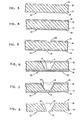
- Figs. 3 through 8 illustrate a sequence of process steps for production of an aperture in a single crystal silicon wafer 10 for forming one fluid nozzle or an array of nozzles. It is to be understood that the following process steps may be used in a different sequence and that other film materials for performing the same functions described below may be used. Furthermore, film formation, size, thickness and the like, may also be varied.
- the wafer 10 is of single crystal (100) oriented p type silicon with electrical resistivity of 0;5 to 100 ohm-cm, approximately 19,5 to 20,5 mils thick having front 14 and back 15 surfaces.
- the (100) planes are parallel to surfaces 14 and 15. As shown in Fig.
- phosphorous is diffused into the front 14 and back 15 surfaces of the silicon wafer 10 to a depth of about 5 microns forming n type layers 16 and 17.
- the diffusion is accomplished in a well-known manner by having a gas mixture containing 0,75 % PH 3 , 1 % 2 0, and the make-up of Ar and N 2 flow for 30 minutes past the silicon wafer 10 which is maintained at 950°C. This is followed by a long drive-in period (1050°C for 22 hours) to achieve a thick layer (about 5 microns). Since the final concentration of phosphorous in the n layers 16 and 17 is very low, this diffusion step introduces very little stress into the silicon wafer 10, and consequently the silicon structure retains its strength.
- both front 14 and back 15 surfaces of the wafer 10 are coated with a protective material such as LPCVD silicon nitride forming layers 18 and 19 which can resist a long etching period in a caustic (KOH) solution.
- a protective material such as LPCVD silicon nitride forming layers 18 and 19 which can resist a long etching period in a caustic (KOH) solution.
- LPCVD silicon nitride forming layers 18 and 19 which can resist a long etching period in a caustic (KOH) solution.
- LPCVD silicon nitride forming layers 18 and 19 which can resist a long etching period in a caustic (KOH) solution.
- Oxide layers (not shown) less than 0,5 microns thick may be grown on both sides of layers 18 and 19 to reduce the effect of stress between nitride and silicon and to improve adhesion of photoresist to nitride.
- masks are prepared corresponding to the desired entrance 20 and exit 21 areas of the nozzle.
- the masks for both entrance 20 and exit 21 areas are made circular in shape since the openings in the silicon wafer 10 defined by circular masks will etch out to squares parallel to the 100 planes, each square circumscribing its respective circle. Use of circular masks eliminates possible error due to the theta misalignment which may occur when a square shaped mask is used.
- the silicon nitride layers 18 and 19 are photoshaped simultaneously on both sides using a two-sided photospinner (not shown) and a two-sided aligner (not shown). The resulting structure after etching away of portions of layers 18 and 19 defining the entrance 20 and exit 21 areas, is shown in Fig. 5.
- the exit area 21 is then protected from the etching solution by covering it with a metallic layer 22, as shown in Fig. 6, or by use of a hermetic mechanical fixture (not shown). Thereafter the wafer is submerged in a hot (80-85°C) KOH solution (not shown) and a potential is placed across the p/n junction at the back side 15 by connecting the positive side of an electrical power source (not shown) with the metallic layer 22 protecting the exit area 21.
- Other alkaline etch solutions such as metal hydroxides of the Group I-A elements of the Periodic Table, for example, NaOH, NH 4 0H, or others, may be used.
- electrochemically controlled thinning process for semi-conductors is well-known in the art and is described in detail in US-A-3,689,389.
- the opening 11 in the monocrystalline silicon wafer 10 is etched anisotropically until the diffused layer 17 at the back side 25 is reached, at which time the etching action stops due to an oxide layer (not shown) which is caused to grow at the p/n junction due to the applied potential across the junction.
- the (111) plane is a slow etch plane in monocrystalline silicon material when a KOH etching solution is used.
- the etching step produces a pyramidal opening in the wafer 10 which opening truncates in a membrane 12 when it encounters the electrochemical etch barrier set up at the silicon and diffused layer 17 interface (p/n junction).
- the wafer 10 is removed from the etching solution, the protective metallic layer 22 and associated electrical connection on the exit side are removed, and the entrance side 20 is protected from the etching solution usually by a layer 24 formed by air oxidation.
- the wafer 10 is then re-submersed into the etching solution and a pyramidal passage is etched anisotropically from the back surface 15 to form the exit opening 13.
- the resulting structure is shown in Fig. 7.
- the protective coatings 18, 19 and 24 are then removed leaving a completed pure silicon nozzle structure as shown in Fig. 8.
- the initial opening of the entrance 20 is about 35 mils wide and the smallest portion of the exit opening 13 is about 1,5 to 4 mils wide.
- the back surface 15 of the wafer 10 may be coated with a material of low surface energy such as Teflon.
Landscapes
- Engineering & Computer Science (AREA)
- Manufacturing & Machinery (AREA)
- Particle Formation And Scattering Control In Inkjet Printers (AREA)
- Weting (AREA)
- Nozzles (AREA)
- Special Spraying Apparatus (AREA)
Applications Claiming Priority (2)
| Application Number | Priority Date | Filing Date | Title |
|---|---|---|---|
| US66100584A | 1984-10-15 | 1984-10-15 | |
| US661005 | 1984-10-15 |
Publications (4)
| Publication Number | Publication Date |
|---|---|
| EP0178596A2 true EP0178596A2 (de) | 1986-04-23 |
| EP0178596A3 EP0178596A3 (en) | 1987-09-16 |
| EP0178596B1 EP0178596B1 (de) | 1991-01-16 |
| EP0178596B2 EP0178596B2 (de) | 1994-06-01 |
Family
ID=24651804
Family Applications (1)
| Application Number | Title | Priority Date | Filing Date |
|---|---|---|---|
| EP85112882A Expired - Lifetime EP0178596B2 (de) | 1984-10-15 | 1985-10-11 | Siliziumdüsenstruktur und Herstellungsverfahren |
Country Status (7)
| Country | Link |
|---|---|
| EP (1) | EP0178596B2 (de) |
| JP (1) | JPS6198558A (de) |
| KR (1) | KR930009109B1 (de) |
| AU (1) | AU582581B2 (de) |
| CA (1) | CA1237020A (de) |
| DE (1) | DE3581355D1 (de) |
| ES (2) | ES8707144A1 (de) |
Cited By (9)
| Publication number | Priority date | Publication date | Assignee | Title |
|---|---|---|---|---|
| EP0317300A3 (en) * | 1987-11-17 | 1990-01-03 | Hewlett-Packard Company | Nozzle plate for an ink jet printer |
| EP0578130A1 (de) * | 1992-07-06 | 1994-01-12 | Heinzl, Joachim, Prof. Dr.-Ing. | Aerostatische Miniaturlager |
| EP0921002A3 (de) * | 1997-12-05 | 1999-12-15 | Canon Kabushiki Kaisha | Flüssigkeitsausstosskopf, Flüssigkeitsausstossgerät und Flüssigkeitsausstossverfahren |
| EP0921004A3 (de) * | 1997-12-05 | 2000-04-26 | Canon Kabushiki Kaisha | Flüssigkeitsausstosskopf , Aufzeichnungsgerät und Flüssigkeitsausstosskopfenherstellungsverfahren |
| US6120131A (en) * | 1995-08-28 | 2000-09-19 | Lexmark International, Inc. | Method of forming an inkjet printhead nozzle structure |
| US6323456B1 (en) | 1995-08-28 | 2001-11-27 | Lexmark International, Inc. | Method of forming an ink jet printhead structure |
| EP1170128A1 (de) * | 2000-06-29 | 2002-01-09 | Eastman Kodak Company | Mehrlagendichtungssammelleitung für Tintenstrahlzuführsysteme und ähnliche Systeme |
| US6375858B1 (en) | 1997-05-14 | 2002-04-23 | Seiko Epson Corporation | Method of forming nozzle for injection device and method of manufacturing inkjet head |
| US6485132B1 (en) | 1997-12-05 | 2002-11-26 | Canon Kabushiki Kaisha | Liquid discharge head, recording apparatus, and method for manufacturing liquid discharge heads |
Families Citing this family (3)
| Publication number | Priority date | Publication date | Assignee | Title |
|---|---|---|---|---|
| KR100944884B1 (ko) * | 2007-11-01 | 2010-03-03 | 주식회사 알파켐 | 비충격 프린팅을 위한 노즐 및 이를 사용한 인쇄방법 |
| JP5407162B2 (ja) * | 2008-04-01 | 2014-02-05 | コニカミノルタ株式会社 | インクジェットヘッド、インクジェットヘッドを備えた塗布装置及びインクジェットヘッドの駆動方法 |
| KR101291689B1 (ko) * | 2010-08-17 | 2013-08-01 | 엔젯 주식회사 | 정전기력을 이용하는 액적분사장치용 노즐 |
Family Cites Families (9)
| Publication number | Priority date | Publication date | Assignee | Title |
|---|---|---|---|---|
| USB789264I5 (de) * | 1969-01-06 | |||
| JPS5040616B1 (de) * | 1970-03-18 | 1975-12-25 | ||
| US3958255A (en) * | 1974-12-31 | 1976-05-18 | International Business Machines Corporation | Ink jet nozzle structure |
| US3921916A (en) * | 1974-12-31 | 1975-11-25 | Ibm | Nozzles formed in monocrystalline silicon |
| US3949410A (en) * | 1975-01-23 | 1976-04-06 | International Business Machines Corporation | Jet nozzle structure for electrohydrodynamic droplet formation and ink jet printing system therewith |
| US4157935A (en) * | 1977-12-23 | 1979-06-12 | International Business Machines Corporation | Method for producing nozzle arrays for ink jet printers |
| JPS5753366A (en) * | 1980-09-17 | 1982-03-30 | Ricoh Co Ltd | Nozzle plate for liquid jet apparatus |
| JPS57116656A (en) * | 1981-01-14 | 1982-07-20 | Sharp Corp | Manufacture of orifice for ink jet printer |
| JPS57182449A (en) * | 1981-05-07 | 1982-11-10 | Fuji Xerox Co Ltd | Forming method of ink jet multinozzle |
-
1985
- 1985-03-27 CA CA000477672A patent/CA1237020A/en not_active Expired
- 1985-10-02 AU AU48190/85A patent/AU582581B2/en not_active Expired
- 1985-10-11 EP EP85112882A patent/EP0178596B2/de not_active Expired - Lifetime
- 1985-10-11 DE DE8585112882T patent/DE3581355D1/de not_active Expired - Lifetime
- 1985-10-14 KR KR1019850007532A patent/KR930009109B1/ko not_active Expired - Fee Related
- 1985-10-14 ES ES547845A patent/ES8707144A1/es not_active Expired
- 1985-10-15 JP JP60227956A patent/JPS6198558A/ja active Pending
-
1987
- 1987-04-13 ES ES1987296483U patent/ES296483Y/es not_active Expired
Cited By (11)
| Publication number | Priority date | Publication date | Assignee | Title |
|---|---|---|---|---|
| EP0317300A3 (en) * | 1987-11-17 | 1990-01-03 | Hewlett-Packard Company | Nozzle plate for an ink jet printer |
| EP0578130A1 (de) * | 1992-07-06 | 1994-01-12 | Heinzl, Joachim, Prof. Dr.-Ing. | Aerostatische Miniaturlager |
| US6120131A (en) * | 1995-08-28 | 2000-09-19 | Lexmark International, Inc. | Method of forming an inkjet printhead nozzle structure |
| US6323456B1 (en) | 1995-08-28 | 2001-11-27 | Lexmark International, Inc. | Method of forming an ink jet printhead structure |
| US6375858B1 (en) | 1997-05-14 | 2002-04-23 | Seiko Epson Corporation | Method of forming nozzle for injection device and method of manufacturing inkjet head |
| US6863375B2 (en) | 1997-05-14 | 2005-03-08 | Seiko Epson Corporation | Ejection device and inkjet head with silicon nozzle plate |
| EP0921002A3 (de) * | 1997-12-05 | 1999-12-15 | Canon Kabushiki Kaisha | Flüssigkeitsausstosskopf, Flüssigkeitsausstossgerät und Flüssigkeitsausstossverfahren |
| EP0921004A3 (de) * | 1997-12-05 | 2000-04-26 | Canon Kabushiki Kaisha | Flüssigkeitsausstosskopf , Aufzeichnungsgerät und Flüssigkeitsausstosskopfenherstellungsverfahren |
| US6485132B1 (en) | 1997-12-05 | 2002-11-26 | Canon Kabushiki Kaisha | Liquid discharge head, recording apparatus, and method for manufacturing liquid discharge heads |
| EP1170128A1 (de) * | 2000-06-29 | 2002-01-09 | Eastman Kodak Company | Mehrlagendichtungssammelleitung für Tintenstrahlzuführsysteme und ähnliche Systeme |
| US6463656B1 (en) | 2000-06-29 | 2002-10-15 | Eastman Kodak Company | Laminate and gasket manfold for ink jet delivery systems and similar devices |
Also Published As
| Publication number | Publication date |
|---|---|
| EP0178596A3 (en) | 1987-09-16 |
| KR860003109A (ko) | 1986-05-19 |
| AU582581B2 (en) | 1989-04-06 |
| ES296483Y (es) | 1988-04-16 |
| KR930009109B1 (ko) | 1993-09-23 |
| ES547845A0 (es) | 1987-08-16 |
| EP0178596B2 (de) | 1994-06-01 |
| CA1237020A (en) | 1988-05-24 |
| AU4819085A (en) | 1986-04-24 |
| EP0178596B1 (de) | 1991-01-16 |
| ES296483U (es) | 1987-10-16 |
| JPS6198558A (ja) | 1986-05-16 |
| ES8707144A1 (es) | 1987-08-16 |
| DE3581355D1 (de) | 1991-02-21 |
Similar Documents
| Publication | Publication Date | Title |
|---|---|---|
| US4733823A (en) | Silicon nozzle structures and method of manufacture | |
| EP0178596B1 (de) | Siliziumdüsenstruktur und Herstellungsverfahren | |
| US3962052A (en) | Process for forming apertures in silicon bodies | |
| CA1114050A (en) | Manufacture of solar cells | |
| DE68918982T2 (de) | Verfahren zur Trennung integrierter Schaltkreise auf einem Substrat. | |
| US5711891A (en) | Wafer processing using thermal nitride etch mask | |
| US5131978A (en) | Low temperature, single side, multiple step etching process for fabrication of small and large structures | |
| US4706374A (en) | Method of manufacture for semiconductor accelerometer | |
| US5286671A (en) | Fusion bonding technique for use in fabricating semiconductor devices | |
| US7169669B2 (en) | Method of making thin silicon sheets for solar cells | |
| US5096535A (en) | Process for manufacturing segmented channel structures | |
| JP2008532319A (ja) | 接合部分離バイア | |
| US4318759A (en) | Retro-etch process for integrated circuits | |
| JPS6043309B2 (ja) | マルチノズルオリフイス板 | |
| US6033489A (en) | Semiconductor substrate and method of making same | |
| US3447235A (en) | Isolated cathode array semiconductor | |
| JPS5760851A (en) | Dielectric isolation of semiconductor integrated circuit | |
| US4334348A (en) | Retro-etch process for forming gate electrodes of MOS integrated circuits | |
| US3661741A (en) | Fabrication of integrated semiconductor devices by electrochemical etching | |
| GB1246294A (en) | Method of manufacturing semiconductor devices | |
| US5445718A (en) | Electrochemical etch-stop on n-type silicon by injecting holes from a shallow p-type layer | |
| EP0050972A2 (de) | Verfahren zum Herstellen eines Halbleiterbauelementes mit einer verbindenden Elektrodenschicht | |
| JPS5772321A (en) | Manufacture of seiconductor device | |
| CN100435272C (zh) | 在感应耦合等离子体刻蚀中保护刻蚀结构的方法 | |
| DE102006042329B4 (de) | Verfahren zum selektiven plasmachemischen Trockenätzen von auf Oberflächen von Silicium-Wafern ausgebildetem Phosphorsilikatglas |
Legal Events
| Date | Code | Title | Description |
|---|---|---|---|
| PUAI | Public reference made under article 153(3) epc to a published international application that has entered the european phase |
Free format text: ORIGINAL CODE: 0009012 |
|
| AK | Designated contracting states |
Kind code of ref document: A2 Designated state(s): BE DE FR GB IT NL |
|
| PUAL | Search report despatched |
Free format text: ORIGINAL CODE: 0009013 |
|
| AK | Designated contracting states |
Kind code of ref document: A3 Designated state(s): BE DE FR GB IT NL |
|
| 17P | Request for examination filed |
Effective date: 19880223 |
|
| 17Q | First examination report despatched |
Effective date: 19890630 |
|
| GRAA | (expected) grant |
Free format text: ORIGINAL CODE: 0009210 |
|
| AK | Designated contracting states |
Kind code of ref document: B1 Designated state(s): BE DE FR GB IT NL |
|
| REF | Corresponds to: |
Ref document number: 3581355 Country of ref document: DE Date of ref document: 19910221 |
|
| ITF | It: translation for a ep patent filed | ||
| ET | Fr: translation filed | ||
| PLBI | Opposition filed |
Free format text: ORIGINAL CODE: 0009260 |
|
| 26 | Opposition filed |
Opponent name: MANNESMANN AKTIENGESELLSCHAFT Effective date: 19911016 |
|
| NLR1 | Nl: opposition has been filed with the epo |
Opponent name: MANNESMANN AKTIENGESELLSCHAFT. |
|
| PLAB | Opposition data, opponent's data or that of the opponent's representative modified |
Free format text: ORIGINAL CODE: 0009299OPPO |
|
| R26 | Opposition filed (corrected) |
Opponent name: MANNESMANN AKTIENGESELLSCHAFT Effective date: 19911016 |
|
| PUAH | Patent maintained in amended form |
Free format text: ORIGINAL CODE: 0009272 |
|
| STAA | Information on the status of an ep patent application or granted ep patent |
Free format text: STATUS: PATENT MAINTAINED AS AMENDED |
|
| 27A | Patent maintained in amended form |
Effective date: 19940601 |
|
| AK | Designated contracting states |
Kind code of ref document: B2 Designated state(s): BE DE FR GB IT NL |
|
| NLR2 | Nl: decision of opposition | ||
| ET3 | Fr: translation filed ** decision concerning opposition | ||
| NLR3 | Nl: receipt of modified translations in the netherlands language after an opposition procedure | ||
| PGFP | Annual fee paid to national office [announced via postgrant information from national office to epo] |
Ref country code: BE Payment date: 19970925 Year of fee payment: 13 |
|
| NLS | Nl: assignments of ep-patents |
Owner name: NCR INTERNATIONAL, INC;AMERICAN TELEPHONE AND TELE |
|
| NLT1 | Nl: modifications of names registered in virtue of documents presented to the patent office pursuant to art. 16 a, paragraph 1 |
Owner name: AT & T CORPORATION |
|
| REG | Reference to a national code |
Ref country code: FR Ref legal event code: TP Ref country code: FR Ref legal event code: CD Ref country code: FR Ref legal event code: CA |
|
| PGFP | Annual fee paid to national office [announced via postgrant information from national office to epo] |
Ref country code: NL Payment date: 19981030 Year of fee payment: 14 |
|
| PG25 | Lapsed in a contracting state [announced via postgrant information from national office to epo] |
Ref country code: BE Free format text: LAPSE BECAUSE OF NON-PAYMENT OF DUE FEES Effective date: 19981031 |
|
| BECA | Be: change of holder's address |
Free format text: 980119 *NCR INTERNATIONAL INC.:1700 SOUTH PATTERSON BOULEVARD, DAYTON, OHIO 45479 |
|
| BECH | Be: change of holder |
Free format text: 980119 *NCR INTERNATIONAL INC.:1700 SOUTH PATTERSON BOULEVARD, DAYTON, OHIO 45479 |
|
| BECN | Be: change of holder's name |
Effective date: 19980119 |
|
| BERE | Be: lapsed |
Owner name: NCR INTERNATIONAL INC. Effective date: 19981031 |
|
| PG25 | Lapsed in a contracting state [announced via postgrant information from national office to epo] |
Ref country code: NL Free format text: LAPSE BECAUSE OF NON-PAYMENT OF DUE FEES Effective date: 20000501 |
|
| REG | Reference to a national code |
Ref country code: GB Ref legal event code: 732E |
|
| NLV4 | Nl: lapsed or anulled due to non-payment of the annual fee |
Effective date: 20000501 |
|
| REG | Reference to a national code |
Ref country code: GB Ref legal event code: IF02 |
|
| REG | Reference to a national code |
Ref country code: GB Ref legal event code: 746 Effective date: 20021024 |
|
| REG | Reference to a national code |
Ref country code: FR Ref legal event code: D6 |
|
| REG | Reference to a national code |
Ref country code: GB Ref legal event code: 747D |
|
| REG | Reference to a national code |
Ref country code: FR Ref legal event code: LT |
|
| REG | Reference to a national code |
Ref country code: GB Ref legal event code: 747D |
|
| PGFP | Annual fee paid to national office [announced via postgrant information from national office to epo] |
Ref country code: GB Payment date: 20041006 Year of fee payment: 20 |
|
| PGFP | Annual fee paid to national office [announced via postgrant information from national office to epo] |
Ref country code: FR Payment date: 20041020 Year of fee payment: 20 |
|
| PGFP | Annual fee paid to national office [announced via postgrant information from national office to epo] |
Ref country code: DE Payment date: 20041130 Year of fee payment: 20 |
|
| PG25 | Lapsed in a contracting state [announced via postgrant information from national office to epo] |
Ref country code: GB Free format text: LAPSE BECAUSE OF EXPIRATION OF PROTECTION Effective date: 20051010 |
|
| REG | Reference to a national code |
Ref country code: GB Ref legal event code: PE20 |
|
| PLAB | Opposition data, opponent's data or that of the opponent's representative modified |
Free format text: ORIGINAL CODE: 0009299OPPO |