EP0175356A2 - Clavier et membranes à circuit - Google Patents
Clavier et membranes à circuit Download PDFInfo
- Publication number
- EP0175356A2 EP0175356A2 EP85111797A EP85111797A EP0175356A2 EP 0175356 A2 EP0175356 A2 EP 0175356A2 EP 85111797 A EP85111797 A EP 85111797A EP 85111797 A EP85111797 A EP 85111797A EP 0175356 A2 EP0175356 A2 EP 0175356A2
- Authority
- EP
- European Patent Office
- Prior art keywords
- contact points
- tracks
- resistance
- conductor
- connection contact
- Prior art date
- Legal status (The legal status is an assumption and is not a legal conclusion. Google has not performed a legal analysis and makes no representation as to the accuracy of the status listed.)
- Granted
Links
Images
Classifications
-
- H—ELECTRICITY
- H05—ELECTRIC TECHNIQUES NOT OTHERWISE PROVIDED FOR
- H05K—PRINTED CIRCUITS; CASINGS OR CONSTRUCTIONAL DETAILS OF ELECTRIC APPARATUS; MANUFACTURE OF ASSEMBLAGES OF ELECTRICAL COMPONENTS
- H05K1/00—Printed circuits
- H05K1/02—Details
- H05K1/0213—Electrical arrangements not otherwise provided for
- H05K1/0237—High frequency adaptations
- H05K1/0246—Termination of transmission lines
-
- H—ELECTRICITY
- H01—ELECTRIC ELEMENTS
- H01H—ELECTRIC SWITCHES; RELAYS; SELECTORS; EMERGENCY PROTECTIVE DEVICES
- H01H13/00—Switches having rectilinearly-movable operating part or parts adapted for pushing or pulling in one direction only, e.g. push-button switch
- H01H13/70—Switches having rectilinearly-movable operating part or parts adapted for pushing or pulling in one direction only, e.g. push-button switch having a plurality of operating members associated with different sets of contacts, e.g. keyboard
- H01H13/702—Switches having rectilinearly-movable operating part or parts adapted for pushing or pulling in one direction only, e.g. push-button switch having a plurality of operating members associated with different sets of contacts, e.g. keyboard with contacts carried by or formed from layers in a multilayer structure, e.g. membrane switches
-
- H—ELECTRICITY
- H05—ELECTRIC TECHNIQUES NOT OTHERWISE PROVIDED FOR
- H05K—PRINTED CIRCUITS; CASINGS OR CONSTRUCTIONAL DETAILS OF ELECTRIC APPARATUS; MANUFACTURE OF ASSEMBLAGES OF ELECTRICAL COMPONENTS
- H05K1/00—Printed circuits
- H05K1/16—Printed circuits incorporating printed electric components, e.g. printed resistor, capacitor, inductor
- H05K1/167—Printed circuits incorporating printed electric components, e.g. printed resistor, capacitor, inductor incorporating printed resistors
-
- H—ELECTRICITY
- H01—ELECTRIC ELEMENTS
- H01H—ELECTRIC SWITCHES; RELAYS; SELECTORS; EMERGENCY PROTECTIVE DEVICES
- H01H2203/00—Form of contacts
- H01H2203/056—Cuts or depressions in support, e.g. to isolate contacts
-
- H—ELECTRICITY
- H01—ELECTRIC ELEMENTS
- H01H—ELECTRIC SWITCHES; RELAYS; SELECTORS; EMERGENCY PROTECTIVE DEVICES
- H01H2239/00—Miscellaneous
- H01H2239/004—High frequency adaptation or shielding
-
- H—ELECTRICITY
- H01—ELECTRIC ELEMENTS
- H01H—ELECTRIC SWITCHES; RELAYS; SELECTORS; EMERGENCY PROTECTIVE DEVICES
- H01H2239/00—Miscellaneous
- H01H2239/01—Miscellaneous combined with other elements on the same substrate
-
- H—ELECTRICITY
- H05—ELECTRIC TECHNIQUES NOT OTHERWISE PROVIDED FOR
- H05K—PRINTED CIRCUITS; CASINGS OR CONSTRUCTIONAL DETAILS OF ELECTRIC APPARATUS; MANUFACTURE OF ASSEMBLAGES OF ELECTRICAL COMPONENTS
- H05K1/00—Printed circuits
- H05K1/02—Details
- H05K1/03—Use of materials for the substrate
- H05K1/0393—Flexible materials
-
- H—ELECTRICITY
- H05—ELECTRIC TECHNIQUES NOT OTHERWISE PROVIDED FOR
- H05K—PRINTED CIRCUITS; CASINGS OR CONSTRUCTIONAL DETAILS OF ELECTRIC APPARATUS; MANUFACTURE OF ASSEMBLAGES OF ELECTRICAL COMPONENTS
- H05K1/00—Printed circuits
- H05K1/02—Details
- H05K1/09—Use of materials for the conductive, e.g. metallic pattern
- H05K1/092—Dispersed materials, e.g. conductive pastes or inks
- H05K1/095—Dispersed materials, e.g. conductive pastes or inks for polymer thick films, i.e. having a permanent organic polymeric binder
-
- H—ELECTRICITY
- H05—ELECTRIC TECHNIQUES NOT OTHERWISE PROVIDED FOR
- H05K—PRINTED CIRCUITS; CASINGS OR CONSTRUCTIONAL DETAILS OF ELECTRIC APPARATUS; MANUFACTURE OF ASSEMBLAGES OF ELECTRICAL COMPONENTS
- H05K1/00—Printed circuits
- H05K1/02—Details
- H05K1/11—Printed elements for providing electric connections to or between printed circuits
- H05K1/118—Printed elements for providing electric connections to or between printed circuits specially for flexible printed circuits, e.g. using folded portions
-
- H—ELECTRICITY
- H05—ELECTRIC TECHNIQUES NOT OTHERWISE PROVIDED FOR
- H05K—PRINTED CIRCUITS; CASINGS OR CONSTRUCTIONAL DETAILS OF ELECTRIC APPARATUS; MANUFACTURE OF ASSEMBLAGES OF ELECTRICAL COMPONENTS
- H05K2201/00—Indexing scheme relating to printed circuits covered by H05K1/00
- H05K2201/03—Conductive materials
- H05K2201/032—Materials
- H05K2201/0323—Carbon
-
- H—ELECTRICITY
- H05—ELECTRIC TECHNIQUES NOT OTHERWISE PROVIDED FOR
- H05K—PRINTED CIRCUITS; CASINGS OR CONSTRUCTIONAL DETAILS OF ELECTRIC APPARATUS; MANUFACTURE OF ASSEMBLAGES OF ELECTRICAL COMPONENTS
- H05K2201/00—Indexing scheme relating to printed circuits covered by H05K1/00
- H05K2201/10—Details of components or other objects attached to or integrated in a printed circuit board
- H05K2201/10007—Types of components
- H05K2201/10053—Switch
-
- Y—GENERAL TAGGING OF NEW TECHNOLOGICAL DEVELOPMENTS; GENERAL TAGGING OF CROSS-SECTIONAL TECHNOLOGIES SPANNING OVER SEVERAL SECTIONS OF THE IPC; TECHNICAL SUBJECTS COVERED BY FORMER USPC CROSS-REFERENCE ART COLLECTIONS [XRACs] AND DIGESTS
- Y10—TECHNICAL SUBJECTS COVERED BY FORMER USPC
- Y10T—TECHNICAL SUBJECTS COVERED BY FORMER US CLASSIFICATION
- Y10T29/00—Metal working
- Y10T29/49—Method of mechanical manufacture
- Y10T29/49002—Electrical device making
- Y10T29/49117—Conductor or circuit manufacturing
- Y10T29/49124—On flat or curved insulated base, e.g., printed circuit, etc.
- Y10T29/49155—Manufacturing circuit on or in base
Definitions
- the invention relates to a keyboard-membrane circuit with switching contact points, which are led in groups to printed circuit traces to connection contact points, the conductive paths running parallel to each other in certain areas and the connection contact points and / or the switching contact points consisting of a carbon resistance layer.
- connection contact points and / or the switching contact points are often constructed from a carbon resistance layer, which is much more resistant to the stresses in operation.
- Coupling capacitances occur between the conductor tracks in such film circuits. In some cases, these have a disruptive effect on the connected electronic circuit.
- the object of the invention is to suppress the influence of the coupling capacitances of the conductor tracks in a film circuit of the type mentioned at the outset and to select and design such suppression measures in such a way that they can be produced using simple means.
- the above object is achieved in a film circuit of the type mentioned at the outset in that resistance tracks are printed on the film in each case between two conductor tracks and connected to them, and in that the resistance tracks consist of the same carbon resistance layer material as the connection contact points or the switching contact points.
- resistors with a certain resistance value between the conductor tracks have an attenuation capacitive coupling. Arrange such resistors discretely or in a separate printing process; would be expensive.
- the resistors consist of the same carbon layer material as the connection contact points or the switching contact points. The switching contact points or the connection contact points and the resistance tracks between the conductor tracks can thus be applied to the film in the same printing process. It is accepted that the resistance tracks are relatively long because a low-resistance resistor paste is used for the connection contact points or the switching contact points and high-resistance resistors are required between the conductor tracks.
- Another advantage is that the resistances between the conductor tracks do not cross them, making them easy to print on the film without an additional insulating layer.
- the resistor tracks are printed in a region between the conductor tracks in which they run parallel to one another and the resistor tracks run parallel to the conductor tracks in their longitudinal extent, each resistor track being connected to the two conductor tracks between which it runs.
- the resistance tracks can be arranged on the film in a space-saving manner.
- the resistance tracks running parallel between the conductor tracks can bring an additional decoupling effect.
- resistors are parallel between n conductor tracks, then only n-1 resistor tracks are necessary.
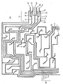
- FIG. 1 shows a foil of a keyboard membrane circuit printed with conductor tracks and resistance tracks, broken off.
- a conductor path 1 leads to switching contact points 2.
- a conductor path 3 leads to switching contact points 4.
- a conductor path 5 leads to switching contact points 6.
- a conductor path 7 leads to switching contact points 8.
- a conductor path 9 leads to switching contact points 10. Since the film is shown broken off in the figure, only some of the switch contact points can be seen.
- the conductor tracks 1, 3, 5, 7 and 9 run parallel in areas 11 and 12. Each conductor track 1, 3, 5, 7 and 9 ends at a contact point 13 to 17. The distance between the connection contact points 13 to 17 corresponds the grid of a common terminal block.
- the conductor tracks 1, 3, 5, 7 and 9 consist of a silver conductive paste printed on the film 18.
- the switching contact points 2, 4, 6, 8, 10 and the connection contact points 13 to 17 are printed on the film 18 from a low-resistance resistor paste.
- resistance tracks 19, 20, 21 and 22 from this resistance paste are printed between conductor tracks 1, 3, 5, 7 and 9.
- the resistance tracks 19 to 22 are parallel in their longitudinal extent to the conductor tracks 1, 3, 5, 7 and 9.
- the resistance track 19 is connected at one end to the conductor track 1 and at its other end to the conductor track 3. The same applies to the other resistance tracks.
- the resistance value of each resistance track is, for example, 9 k11.
- the resistance tracks 19 to 22 are long compared to the switch contact points 2, 4, 6, 8 and 10 and the connection contact points 13 to 17.
- Resistance tracks of the type mentioned can also be arranged additionally or alternatively in the area 12.
- connection contact points 13, 14, 16 and 17 Since the one ends of the resistance tracks 19, 20, 21 and 22 are already very close to the connection contact points 13, 14, 16 and 17, these connection contact points and the resistance tracks can be printed throughout without the connection points and the Resistance traces there are conductor track sections. The conductor tracks then branch off directly from the continuous resistance track.
- the series connection of the resistor tracks 19 to 22 is electrically between the outer conductor tracks 1 and 9. If an additional resistance between the conductor tracks 1 and 9 is desired, this can be provided without intersection between the point 23 of the conductor track 1 and the point 24 of the conductor track 9.
Landscapes
- Engineering & Computer Science (AREA)
- Microelectronics & Electronic Packaging (AREA)
- Push-Button Switches (AREA)
- Contacts (AREA)
- Parts Printed On Printed Circuit Boards (AREA)
Applications Claiming Priority (2)
| Application Number | Priority Date | Filing Date | Title |
|---|---|---|---|
| DE3434664 | 1984-09-21 | ||
| DE19843434664 DE3434664A1 (de) | 1984-09-21 | 1984-09-21 | Tastatur-folienschaltung |
Publications (3)
| Publication Number | Publication Date |
|---|---|
| EP0175356A2 true EP0175356A2 (fr) | 1986-03-26 |
| EP0175356A3 EP0175356A3 (en) | 1988-11-30 |
| EP0175356B1 EP0175356B1 (fr) | 1991-08-21 |
Family
ID=6245964
Family Applications (1)
| Application Number | Title | Priority Date | Filing Date |
|---|---|---|---|
| EP85111797A Expired - Lifetime EP0175356B1 (fr) | 1984-09-21 | 1985-09-18 | Clavier et membranes à circuit |
Country Status (4)
| Country | Link |
|---|---|
| US (1) | US4658235A (fr) |
| EP (1) | EP0175356B1 (fr) |
| JP (1) | JPS6178194A (fr) |
| DE (1) | DE3434664A1 (fr) |
Families Citing this family (6)
| Publication number | Priority date | Publication date | Assignee | Title |
|---|---|---|---|---|
| USRE34395E (en) * | 1989-06-15 | 1993-10-05 | Cray Research, Inc. | Method of making a chip carrier with terminating resistive elements |
| US4949453A (en) * | 1989-06-15 | 1990-08-21 | Cray Research, Inc. | Method of making a chip carrier with terminating resistive elements |
| DE4244815C2 (de) * | 1991-02-04 | 1997-04-10 | Motorola Inc | Tastenblockschaltung |
| US5409401A (en) * | 1992-11-03 | 1995-04-25 | The Whitaker Corporation | Filtered connector |
| GB9807616D0 (en) * | 1998-04-08 | 1998-06-10 | Weatherley Richard | Reduction of crosstalk in data transmission system |
| DE102005002149A1 (de) * | 2005-01-17 | 2006-07-20 | Printed Systems Gmbh | Tastatur und Verfahren zur Herstellung einer Tastatur |
Citations (1)
| Publication number | Priority date | Publication date | Assignee | Title |
|---|---|---|---|---|
| US4440990A (en) * | 1982-05-19 | 1984-04-03 | Smk Electronics Corporation, Usa | Membrane keyboard assembly |
Family Cites Families (3)
| Publication number | Priority date | Publication date | Assignee | Title |
|---|---|---|---|---|
| US3384931A (en) * | 1966-06-24 | 1968-05-28 | Ibm | Injection printing of electrical circuit components |
| US3766308A (en) * | 1972-05-25 | 1973-10-16 | Microsystems Int Ltd | Joining conductive elements on microelectronic devices |
| JPS595935Y2 (ja) * | 1979-08-08 | 1984-02-23 | アルプス電気株式会社 | 厚膜印刷回路 |
-
1984
- 1984-09-21 DE DE19843434664 patent/DE3434664A1/de active Granted
-
1985
- 1985-09-18 US US06/777,165 patent/US4658235A/en not_active Expired - Fee Related
- 1985-09-18 EP EP85111797A patent/EP0175356B1/fr not_active Expired - Lifetime
- 1985-09-19 JP JP60205482A patent/JPS6178194A/ja active Pending
Patent Citations (1)
| Publication number | Priority date | Publication date | Assignee | Title |
|---|---|---|---|---|
| US4440990A (en) * | 1982-05-19 | 1984-04-03 | Smk Electronics Corporation, Usa | Membrane keyboard assembly |
Also Published As
| Publication number | Publication date |
|---|---|
| DE3434664C2 (fr) | 1991-05-16 |
| DE3434664A1 (de) | 1986-04-03 |
| EP0175356B1 (fr) | 1991-08-21 |
| JPS6178194A (ja) | 1986-04-21 |
| EP0175356A3 (en) | 1988-11-30 |
| US4658235A (en) | 1987-04-14 |
Similar Documents
| Publication | Publication Date | Title |
|---|---|---|
| DE2005565C3 (de) | Als gedruckte Schaltung ausgeführte Schalterplatte und Verfahren zur Herstellung derselben | |
| DE69633848T2 (de) | Leiterplattenfunkenstrecke | |
| EP0712267A2 (fr) | Installation de commande modulaire avec connexion sur bus secteur intégré | |
| EP0955691A2 (fr) | Dispositif de contact | |
| DE2910451A1 (de) | Schalttafel mit kapazitiven beruehrungstasten und verfahren zu deren herstellung | |
| EP0495540B1 (fr) | Plaquette à circuits imprimés à plusieurs niveaux, notamment pour haute fréquence | |
| EP0175356B1 (fr) | Clavier et membranes à circuit | |
| DE3338749A1 (de) | Tastatur | |
| DE2110481B2 (de) | Thermodruckkopf | |
| DE2836092A1 (de) | Elektrische baugruppe mit einer flexiblen gefalteten leiterfolie | |
| DE3821562C1 (fr) | ||
| EP0176082A2 (fr) | Dispositif de raccordement de membrane de clavier | |
| EP0361285B1 (fr) | Carte à circuit capacitif | |
| DE2309869A1 (de) | Schaltung in dickfilm-technik | |
| EP0784344A1 (fr) | Structure semi-conductrice pour l'obtention des réseaux résistifs | |
| DE1515846B1 (de) | Uebertragungsleitung mitkleinem Wellenwiderstand | |
| EP0679051A2 (fr) | Raccordement de moyens d'actionnement et d'affichage | |
| DE4426908B4 (de) | Schaltungsanordnung mit kapazitiven Koppelelementen zur galvanischen Trennung zweier Signal-Stromkreise | |
| DE2333191C2 (de) | Elektronisches Halbleiter-Koppelpunktpaar | |
| DE2755205A1 (de) | Ueber einen schleifkontakt veraenderbarer widerstand | |
| DE1766474B1 (de) | Stromzufuehrleitung fuer in gedruckten Schaltungen angeordnete integrierte Schaltkreise | |
| DE4017263C2 (fr) | ||
| DE2727522A1 (de) | Sensorschaltfeld, insbesondere fuer einen fernsehempfaenger | |
| DE19834381C2 (de) | Leiterplatte | |
| DE2623640A1 (de) | Elektrischer schichtwiderstand und verfahren zu seiner herstellung |
Legal Events
| Date | Code | Title | Description |
|---|---|---|---|
| PUAI | Public reference made under article 153(3) epc to a published international application that has entered the european phase |
Free format text: ORIGINAL CODE: 0009012 |
|
| AK | Designated contracting states |
Kind code of ref document: A2 Designated state(s): AT BE CH FR GB IT LI LU NL SE |
|
| PUAL | Search report despatched |
Free format text: ORIGINAL CODE: 0009013 |
|
| AK | Designated contracting states |
Kind code of ref document: A3 Designated state(s): AT BE CH FR GB IT LI LU NL SE |
|
| 17P | Request for examination filed |
Effective date: 19881224 |
|
| RAP1 | Party data changed (applicant data changed or rights of an application transferred) |
Owner name: PREH-WERKE GMBH & CO. KG |
|
| 17Q | First examination report despatched |
Effective date: 19900705 |
|
| RBV | Designated contracting states (corrected) |
Designated state(s): FR GB IT |
|
| GRAA | (expected) grant |
Free format text: ORIGINAL CODE: 0009210 |
|
| AK | Designated contracting states |
Kind code of ref document: B1 Designated state(s): FR GB IT |
|
| ET | Fr: translation filed | ||
| ITF | It: translation for a ep patent filed |
Owner name: DR. ING. A. RACHELI & C. |
|
| GBT | Gb: translation of ep patent filed (gb section 77(6)(a)/1977) | ||
| PLBE | No opposition filed within time limit |
Free format text: ORIGINAL CODE: 0009261 |
|
| STAA | Information on the status of an ep patent application or granted ep patent |
Free format text: STATUS: NO OPPOSITION FILED WITHIN TIME LIMIT |
|
| 26N | No opposition filed | ||
| PGFP | Annual fee paid to national office [announced via postgrant information from national office to epo] |
Ref country code: GB Payment date: 19940818 Year of fee payment: 10 |
|
| PGFP | Annual fee paid to national office [announced via postgrant information from national office to epo] |
Ref country code: FR Payment date: 19940902 Year of fee payment: 10 |
|
| PG25 | Lapsed in a contracting state [announced via postgrant information from national office to epo] |
Ref country code: GB Effective date: 19950918 |
|
| GBPC | Gb: european patent ceased through non-payment of renewal fee |
Effective date: 19950918 |
|
| PG25 | Lapsed in a contracting state [announced via postgrant information from national office to epo] |
Ref country code: FR Effective date: 19960531 |
|
| REG | Reference to a national code |
Ref country code: FR Ref legal event code: ST |