EP0173439B1 - Luminanz-Chrominanzsignal-Trennstufe - Google Patents
Luminanz-Chrominanzsignal-Trennstufe Download PDFInfo
- Publication number
- EP0173439B1 EP0173439B1 EP85304976A EP85304976A EP0173439B1 EP 0173439 B1 EP0173439 B1 EP 0173439B1 EP 85304976 A EP85304976 A EP 85304976A EP 85304976 A EP85304976 A EP 85304976A EP 0173439 B1 EP0173439 B1 EP 0173439B1
- Authority
- EP
- European Patent Office
- Prior art keywords
- signal
- output signal
- level
- receiving
- output
- Prior art date
- Legal status (The legal status is an assumption and is not a legal conclusion. Google has not performed a legal analysis and makes no representation as to the accuracy of the status listed.)
- Expired
Links
Images


Classifications
-
- H—ELECTRICITY
- H04—ELECTRIC COMMUNICATION TECHNIQUE
- H04N—PICTORIAL COMMUNICATION, e.g. TELEVISION
- H04N9/00—Details of colour television systems
- H04N9/77—Circuits for processing the brightness signal and the chrominance signal relative to each other, e.g. adjusting the phase of the brightness signal relative to the colour signal, correcting differential gain or differential phase
- H04N9/78—Circuits for processing the brightness signal and the chrominance signal relative to each other, e.g. adjusting the phase of the brightness signal relative to the colour signal, correcting differential gain or differential phase for separating the brightness signal or the chrominance signal from the colour television signal, e.g. using comb filter
Definitions
- This invention relates generally to an apparatus for separating a signal from a composite signal formed of two signals and, more particularly to an apparatus for separating a chrominance signal from a composite video signal made up of a luminance signal and the chrominance signal, for use in a color television receiver or a video tape recorder.
- a composite color video signal ultimately requires the separation of its component signals at the time of display, or at the time of recording if they are to be recorded separately, and the systems to accomplish such separation known heretofore typically employ various kinds of filters to separate the luminance signal and the chrominance signal from the composite video.
- filters to separate the luminance signal and the chrominance signal from the composite video.
- An example of such kinds of filtering is the so-called comb filter used in conjunction with a bandpass filter.
- horizontal correlators in conjunction with these signal separating filters. These horizontal correlators involve the delaying of the composite signal to derive a number of signals and then comparing the relative amplitudes of various signals to a reference level signal to produce a correlated output.
- a principal problem to date with the use of a bandpass filter as the luminance/chrominance separator is that a high-frequency cross-talk component of the luminance signal cannot be removed by such bandpass filter because it is of so high a frequency that it is in the filter passband required by the chrominance signal.
- This high-frequency luminance cross-talk is the so-called cross-color component.
- the use of the horizontal correlator has been required in order to provide optimum signal separation in addition to using conventional filtering.
- the delay lines employed in the horizontal correlator necessitate the loss of a portion of the chrominance signal at the time of separation. This signal loss occurs each time the chrominance signal is separated from the composite and if this horizontal correlator is used with video tape recorder equipment, in which the chrominance signal can be separated from the composite video a number of times in performance of a typical editing operation, the usable chrominance signal is reduced at each separation. Thus, the color information that is available is correspondingly diminished to an unacceptable level.
- Another object of this invention is to provide a luminance/chrominance separator in which the signals are separated from the composite video signal such that no component of the luminance signal appears in the chrominance signal.
- a further object of this invention is to provide a luminance/chrominance separator in which the usable extent of the chrominance signal is not diminished following the separation operation.
- two chroma separator units are employed in succession to eliminate the high-frequency luminance cross-talk component from the chrominance.
- the respective input signal is time delayed and then synthesized using level detecting processing before being combined by using nonadding mixers, an output chrominance signal having a length as long as the corresponding portion of the original chrominance signal is produced.
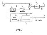
- the composite video signal S v is applied through an input terminal 1 to a luminance separator circuit 2.
- the composite video signal is fed both to a time delay unit 3, which imparts a time delay equal to one horizontal scan period, and also to one input of a signal adder 4.
- the delayed composite signal is then fed through an amplifier 5 to another input of the signal adder 4 and the summed output signal is then passed through a low pass filter 6 to eliminate all but the luminance signal components.
- the separated luminance signal Sy is available at output terminal 7.
- the use of only a bandpass filter to separate luminance and chrominance components of the composite video signal is ineffective to remove a high-frequency cross-talk component of the luminance signal, typically referred to as cross-color, from the chrominance signal, and that component is designated herein as Y H .
- the output of a bandpass filter 8 to which the composite video signal S v is applied will be the chrominance component plus this high-frequency cross-color component (S v + Y H ).
- the resultant signal from bandpass filter 8 is fed to a horizontal correlator 9, which is intended to eliminate the cross-color component.
- Bandpass filter 8 and horizontal correlator 9 make up a chrominance separator unit 10 that has been previously proposed that produces the chrominance signal at output terminal 11.
- Horizontal correlator 9 is not perfect and some noise and a portion of the cross-color typically still remains, but most importantly the above-mentioned problem of losing a portion of the chrominance signal each time the composite video signal is passed through this horizontal correlator is present, thereby leading to a dimination of the usable chrominance signal each time the composite video signal is passed through the horizontal correlator.
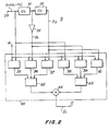
- Horizontal correlator 9 of Fig. 1 is shown in more detail in Fig. 2, in which it is seen that the . input signal S 1 is applied at input terminal 29, and this signal represents the chrominance component S c plus the high-frequency cross-color component Y H .
- Signal S 1 is fed to a delay line 31 that has a time delay corresponding to the period of 1/2 of the wavelength of the subcarrier signal that is modulated by the actual baseband chrominance information when forming the composite video signal, and the output of delay line 31 is fed to a second delay line 32 that provides the same time delay as time delay unit 31.
- the output of first time delay unit 31 is also fed to a signal inverter 34, which inverts the sense or polarity of signals applied thereto.
- the output of inverter 34 is denoted as signal S 2
- the output of second delay line 32 is denoted as signal S 3
- the waveforms of both of these signals are shown in Figs. 3B and 3C, respectively.
- the three signals having relative mutual time delays therebetween, S 1 , S 2 , and S 3 are fed to three maximum detecting circuits 35, 36, and 37, respectively. Additionally, signals S ll S 2 , and S 3 are also fed to three minimum detecting circuits 38, 39, and 40, respectively.
- the maximum and minimum detections take place in relation to a reference signal, and in the horizontal correlator of Fig. 2 a reference signal having a zero voltage level is applied at terminal 41 and is fed to maximum detecting circuits 35, 36, and 37 and also to minimum detecting circuits 38, 39, and 40.
- the reference level input terminal 41 is not shown in separator 10 of Fig. 1 in the interest of clarity.
- maximum detection circuits 35, 36, and 37 are fed to respective inputs of a fourth minimum detection circuit 42, which operates to detect the one input signal having the lowest level among the positive signals detected by maximum detection circuits 35, 36, and 37 and to produce an output signal corresponding to such detection.
- minimum detection circuits 38, 39, and 40 produce outputs fed to respective inputs of a fourth maximum detection circuit 43, which operates to detect the one having the highest level of the negative going signals as detected by minimum detectors 38, 39, and 40 and to produce an output signal corresponding to such detection.
- the output signal of minimum detection circuit 42 and the output signal of maximum detection circuit 43 are fed to adder 44 to produce an output signal that is intended to be void of the so-called cross-color luminance component and such output signal is then provided at output terminal 11.
- the minimum and maximum detecting circuits and the mixer can be referred to as a synthesizer or nonadditive mixer 45.
- Fig. 3A The portion of the input signal S 1 applied to terminal 29 is the chrominance signal Sc, which includes the high-frequency cross-talk component Y H that would be passed by bandpass filter 8 in the circuit of Fig. 1, is represented in Fig. 3A, and Fig. 3B represents the waveform of signal S 2 that has been passed by delay line 31 and inverted by inverter unit 34. Note the shift of the left-most half wavelength, because the signal has been delayed by the delay line 31, and that the high-frequency cross-talk component Y H is now present as a negative-going spike due to inverter 34. Similarly, Fig.
- FIG. 3C represents the waveform of signal S 3 , which has been delayed one complete subcarrier wavelength and, once again, the undesired high-frequency cross-color component Y H is still present.
- the respective signals, shown in Figs. 3A, 3B, and 3C have been processed by .the maximum and minimum circuit elements they are mixed in mixer 44, and the waveform of the resultant signal S 4 is shown in Fig. 3D.
- Fig. 3D clearly shows the principal drawback of this known prior art horizontal correlator in that a portion of the resultant signal is lost due to the requirement to employ delay lines to develop the signal that are checked against the reference level in the various maximum and minimum circuits, and this lost chrominance signal portion is identified as such in Fig 3D. Accordingly, the present invention is intended to overcome this drawback and to substantially reduce the high-frequency cross-color component without losing any of the chrominance signal following the separation operation.
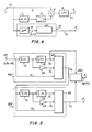
- FIG. 4 An embodiment of the present invention is shown in Fig. 4, in which the horizontal correlator 9 of Fig. 1 is replaced by a chroma separator 46 that produces the desired chrominance output signal S c at output terminal 11.
- the chroma separator 46 of Fig. 4 is shown in more detail in Fig. 5.
- Chroma separator 46 is formed of a first unit 46A, which is substantially the same as the horizontal correlator 9 shown in detail in Fig. 2, however, the output signal thereof is fed to a second unit 46B.
- This second unit 46B is shown in detail in Fig. 6 and differs from the circuit of Fig. 2 in the reversal of the minimum and maximum circuits 42 and 43, respectively.
- the input signal S 1 having the high-frequency cross-talk luminance component therein is fed to first delay line 31 and the output thereof is fed both to second delay unit 32 and to inverter 34, whereby the output of second delay unit 32 forming signal S 3 and the output of inverter 34 forming signal S 2 .
- Both time delay lines produce a time delay equal to the period of 1/2 wavelength of the chrominance subcarrier signal.
- Signals S 1 , S 2 , and S 3 are fed to synthesizer (NAM) 45.
- Synthesizer 45 is essentially the same as that shown in Fig.
- second unit 46B which has a first delay line 51 receiving the signal S 4 , with the output of first delay line 51 being fed both to a second delay line 52 and to an inverter 54.
- the output of second delay line 52 which forms signal S 6 , is fed to synthesizer (NAM) 53, and the output signal S 5 of inverter 54 is also fed to another input of synthesizer 53, whereas signal S 4 is fed directly to another input of the synthesizer 46.
- NAM synthesizer
- S 5 of inverter 54 is also fed to another input of synthesizer 53, whereas signal S 4 is fed directly to another input of the synthesizer 46.
- This embodiment of the present invention has been found to provide acceptable performance without the use of delay lines 32 and 52.
- the outputs of the first delay lines 31, 57 could be connected directly to synthesizers 45, 53, respectively.
- Second unit 46B and synthesizer 53 are shown in detail in Fig. 6, in which it is seen that a maximum circuit 55 is provided in place of the minimum circuit 42 in the correlator of Fig. 2 and a minimum circuit 56 is provided in place of the original maximum circuit 43 in the correlator of Fig. 2.
- the synthesizer (NAM) 53 will differ functionally from the synthesizer 45 utilized in the first unit 46A, and in the previously proposed horizontal correlator 9.
- the output signal S 7 from mixer 44 can be taken directly as the system output, as shown by the dashed lined leading to output terminal 11, in the embodiment of Fig. 5. In the interest of clarity in Fig. 5, the reference signal input terminals 41 have been omitted.
- the output signal S 7 can be checked against a delayed version S 3 of the original input signal in a selector circuit 46C, which functions essentially as another synthesizer or nonadditive mixer.
- This selector circuit 46C is shown in detail in Fig. 7 and functions to select the lesser of the two signals S 3 and S 7 that are input thereto. Because selector circuit 46C selects the lesser of the two signals fed thereto it will normally select signal S 7 , but in the event that signal S 7 would have noise spikes that would make it unusable, selector circuit 46C would select signal S 3 and the overall chrominance signal would not be excessively adversely affected. It is noted that typically signal S 7 will be almost the same as signal S 3 , and the lesser level is caused by the additional signal processing in second unit 46B.
- Fig. 7 it is seen that input signal S 7 is fed to maximum circuit 35, and to minimum circuit 38 and input signal S 3 is fed to maximum circuit 36 and to minimum circuit 37, wherein both input signals are checked against the reference level, which in this case again is a zero voltage level applied at terminal 41. As in the previous embodiments this zero reference level input is not shown in Fig. 5.
- the outputs of maximum detecting circuits 35, 36 are fed to minimum detecting circuit 42, and the outputs of minimum detecting circuits 38, 39 are fed to maximum detecting circuit 43. Based on the above explanation of the operation of these circuits it is seen that this will result in reproducing the input signal having the lowest level.
- the outputs of minimum detecting circuit 42 and maximum detecting circuit 43 are nonadditively combined in mixer 44 to produce output signal S. at terminal 11.
- signal S 4 becomes the input signal to second chroma separator unit 46B shown in Fig. 6 and, particularly, to delay elements 51 and 52, which then delay this signal to form the multiple signals applied to synthesizer (NAM) 53.
- NAM synthesizer
- signal S 7 is the waveform in Fig. 8G, and this signal is made up of all of the highest positive-going portions present in signals S 4 , S 5 , and S 6 and of all of the lowest negative-going portions in those same signals.
- this signal S 7 can also be fed to selector circuit 46C, which operates to select the lower level signal of the two input signals fed thereto, that is, signal S 7 from the chroma separator 46B and signal S 3 , which is the output of second delay line 32 in chroma separator 46B.
- Selector circuit 46C then produces signal S 8 shown in Fig. 8H, which is substantially a pure chrominance signal having the same length as the original input signal S l .
- the comparison of the two signals in selector circuit 46C should take place over a controlled period and this is so labelled in Fig. 8H.
- FIG. 9 A further embodiment of the invention is shown in Fig. 9 in which the bandpass filter 7 and the chroma separator 46 are reversed in serial position, and in this embodiment the output S c , whether taken from signal S 7 or Signal S 8 , still provides a substantially pure chrominance signal having the desired length. Because the high-frequency cross-color component is removed by the chroma separator, the bandpass filter 7 can adequately remove the rest of the luminance signal from the composite video and pass only the chrominance signal.
Landscapes
- Engineering & Computer Science (AREA)
- Multimedia (AREA)
- Signal Processing (AREA)
- Processing Of Color Television Signals (AREA)
- Electrochromic Elements, Electrophoresis, Or Variable Reflection Or Absorption Elements (AREA)
- Non-Silver Salt Photosensitive Materials And Non-Silver Salt Photography (AREA)
Claims (9)
Priority Applications (1)
| Application Number | Priority Date | Filing Date | Title |
|---|---|---|---|
| AT85304976T ATE46800T1 (de) | 1984-07-11 | 1985-07-11 | Luminanz-chrominanzsignal-trennstufe. |
Applications Claiming Priority (2)
| Application Number | Priority Date | Filing Date | Title |
|---|---|---|---|
| JP59144071A JPH0669227B2 (ja) | 1984-07-11 | 1984-07-11 | Y/c分離器 |
| JP144071/84 | 1984-07-11 |
Publications (2)
| Publication Number | Publication Date |
|---|---|
| EP0173439A1 EP0173439A1 (de) | 1986-03-05 |
| EP0173439B1 true EP0173439B1 (de) | 1989-09-27 |
Family
ID=15353607
Family Applications (1)
| Application Number | Title | Priority Date | Filing Date |
|---|---|---|---|
| EP85304976A Expired EP0173439B1 (de) | 1984-07-11 | 1985-07-11 | Luminanz-Chrominanzsignal-Trennstufe |
Country Status (6)
| Country | Link |
|---|---|
| US (1) | US4661842A (de) |
| EP (1) | EP0173439B1 (de) |
| JP (1) | JPH0669227B2 (de) |
| AT (1) | ATE46800T1 (de) |
| CA (1) | CA1229913A (de) |
| DE (1) | DE3573365D1 (de) |
Cited By (3)
| Publication number | Priority date | Publication date | Assignee | Title |
|---|---|---|---|---|
| GB2216745A (en) * | 1988-03-02 | 1989-10-11 | Toshiba Kk | Circuit for separating composite color television signal into luminance signal and chrominance signal |
| EP0358453A2 (de) * | 1988-09-06 | 1990-03-14 | Sony Corporation | Digitale Vorrichtung zur Trennung von Luminanz und Chrominanz |
| US5001553A (en) * | 1988-02-15 | 1991-03-19 | Victor Company Of Japan, Ltd. | Luminance signal/color signal separation circuit |
Families Citing this family (12)
| Publication number | Priority date | Publication date | Assignee | Title |
|---|---|---|---|---|
| JPS62152292A (ja) * | 1985-12-26 | 1987-07-07 | Matsushita Electric Ind Co Ltd | 映像信号記録再生装置 |
| JPH07121136B2 (ja) * | 1987-06-05 | 1995-12-20 | 日本ビクター株式会社 | 映像信号処理回路 |
| US5099314A (en) * | 1987-09-11 | 1992-03-24 | Victor Company Of Japan, Ltd. | Luminance signal/color signal separation circuit |
| US5012329A (en) * | 1989-02-21 | 1991-04-30 | Dubner Computer Systems, Inc. | Method of encoded video decoding |
| JPH0427434A (ja) * | 1990-05-23 | 1992-01-30 | Mitsubishi Heavy Ind Ltd | メタノール改質用触媒 |
| JPH0485778A (ja) * | 1990-07-27 | 1992-03-18 | Victor Co Of Japan Ltd | 磁気テープ強度測定評価方法及び薄手磁気テープ |
| JP2591275B2 (ja) * | 1990-07-27 | 1997-03-19 | 日本ビクター株式会社 | 磁気テープ強度測定評価方法及び磁気テープ強度測定評価装置 |
| JPH04223785A (ja) * | 1990-12-26 | 1992-08-13 | Sony Corp | 映像信号補間処理方法 |
| US5157697A (en) * | 1991-03-21 | 1992-10-20 | Novatel Communications, Ltd. | Receiver employing correlation technique for canceling cross-talk between in-phase and quadrature channels prior to decoding |
| JPH0746150A (ja) * | 1993-07-31 | 1995-02-14 | Nec Corp | 無線選択呼出受信機 |
| JP3076810B2 (ja) * | 1994-01-20 | 2000-08-14 | モトローラ株式会社 | 垂直輪郭補正回路 |
| JPH07226956A (ja) * | 1994-02-09 | 1995-08-22 | Nippon Motorola Ltd | 輝度信号色信号分離回路 |
Family Cites Families (3)
| Publication number | Priority date | Publication date | Assignee | Title |
|---|---|---|---|---|
| JPH0799804B2 (ja) * | 1981-07-13 | 1995-10-25 | ソニー株式会社 | フィルタ装置 |
| JPS5850883A (ja) * | 1981-09-21 | 1983-03-25 | Sony Corp | 分離フイルタ |
| JPS58157285A (ja) * | 1982-03-15 | 1983-09-19 | Victor Co Of Japan Ltd | 搬送色信号の雑音低減回路 |
-
1984
- 1984-07-11 JP JP59144071A patent/JPH0669227B2/ja not_active Expired - Lifetime
-
1985
- 1985-07-10 US US06/753,573 patent/US4661842A/en not_active Expired - Fee Related
- 1985-07-10 CA CA000486605A patent/CA1229913A/en not_active Expired
- 1985-07-11 DE DE8585304976T patent/DE3573365D1/de not_active Expired
- 1985-07-11 AT AT85304976T patent/ATE46800T1/de not_active IP Right Cessation
- 1985-07-11 EP EP85304976A patent/EP0173439B1/de not_active Expired
Cited By (6)
| Publication number | Priority date | Publication date | Assignee | Title |
|---|---|---|---|---|
| US5001553A (en) * | 1988-02-15 | 1991-03-19 | Victor Company Of Japan, Ltd. | Luminance signal/color signal separation circuit |
| EP0525818A1 (de) * | 1988-02-15 | 1993-02-03 | Victor Company Of Japan, Ltd. | Leuchtdichten-/Farbsignal Trennschaltung |
| GB2216745A (en) * | 1988-03-02 | 1989-10-11 | Toshiba Kk | Circuit for separating composite color television signal into luminance signal and chrominance signal |
| GB2216745B (en) * | 1988-03-02 | 1992-09-09 | Toshiba Kk | Circuit for separating composite color television signal into luminance signal and chrominance signal |
| EP0358453A2 (de) * | 1988-09-06 | 1990-03-14 | Sony Corporation | Digitale Vorrichtung zur Trennung von Luminanz und Chrominanz |
| EP0358453A3 (de) * | 1988-09-06 | 1992-04-22 | Sony Corporation | Digitale Vorrichtung zur Trennung von Luminanz und Chrominanz |
Also Published As
| Publication number | Publication date |
|---|---|
| EP0173439A1 (de) | 1986-03-05 |
| JPS6123492A (ja) | 1986-01-31 |
| ATE46800T1 (de) | 1989-10-15 |
| US4661842A (en) | 1987-04-28 |
| DE3573365D1 (en) | 1989-11-02 |
| JPH0669227B2 (ja) | 1994-08-31 |
| CA1229913A (en) | 1987-12-01 |
Similar Documents
| Publication | Publication Date | Title |
|---|---|---|
| EP0173439B1 (de) | Luminanz-Chrominanzsignal-Trennstufe | |
| US5686972A (en) | Circuit for adaptively separating luminance and color signals based on expended vertical and horizontal correlations and method therefor | |
| US4688080A (en) | Multi-standard adaptive chrominance separator | |
| US4809060A (en) | Hanging dot reduction arrangement | |
| US4343017A (en) | Decoding composite PAL television signals | |
| KR0155367B1 (ko) | 3라인 논리콤필터를 사용한 휘도신호/컬러신호 분리회로 및 잡음 감소 회로 | |
| US4731675A (en) | Dropout correcting apparatus wherein dropout detecting flog signal is superimposed on reproduced video signal | |
| EP0199602B1 (de) | Signalverarbeitungsschaltung | |
| KR100642083B1 (ko) | 표준ㆍ비표준신호 판정회로 | |
| US5627600A (en) | Luminance and chrominance signal separator using correlation detection | |
| JP2529834B2 (ja) | ビデオ信号処理装置 | |
| KR940005177B1 (ko) | 펄스패턴 억압회로를 사용하는 필터회로를 갖는 휘도/색신호 분리회로 | |
| KR940004511B1 (ko) | 브이씨알의 재생 색신호 자동 보정 시스템 | |
| US5223943A (en) | Still-video signal playback apparatus with plural system demodulator and low pass filter selection and delay compensation | |
| JPH02186787A (ja) | Y/c分離回路 | |
| EP0420184B1 (de) | Videosignalverarbeitungsschaltung | |
| JPH03187697A (ja) | Yc分離回路 | |
| KR0156850B1 (ko) | 레이저 디스크 플레이어 시스템의 엔티에스시/팔겸용 노이즈 제거회로 | |
| KR900005604B1 (ko) | 상관검출장치와 그것을 사용한 영상신호 기록재생장치 | |
| EP0462746A2 (de) | Automatisches Wiedergabesystem eines Videokassettenrecorders | |
| JPS6358437B2 (de) | ||
| JPH01162090A (ja) | 色信号のクロストーク除去回路 | |
| EP0722254A2 (de) | Vorrichtung zum Ausgleich der Verzögerungszeit für PAL Plus Videorecorder | |
| KR19990002921A (ko) | 휘도 및 색 신호 분리 방법 및 이를 수행하기 위한 휘도 및 색신호 분리 회로 | |
| JPH08265794A (ja) | コンポジットビデオ信号の判定システム |
Legal Events
| Date | Code | Title | Description |
|---|---|---|---|
| PUAI | Public reference made under article 153(3) epc to a published international application that has entered the european phase |
Free format text: ORIGINAL CODE: 0009012 |
|
| 17P | Request for examination filed |
Effective date: 19850716 |
|
| AK | Designated contracting states |
Kind code of ref document: A1 Designated state(s): AT DE FR GB NL |
|
| XX | Miscellaneous (additional remarks) |
Free format text: EIN ANTRAG NACH REGEL 88 EPUE AUF HINZUFUEGUNG DER ANSPRUECHE 3,4,5,6 LIEGT VOR. UEBER DIESER ANTRAG WIRD IM LAUFE DES VERFAHRENS VON DER PRUEFUNGSABTEILUNG EINE ENTSCHEIDUNG GETROFFEN WERDEN. |
|
| 17Q | First examination report despatched |
Effective date: 19880915 |
|
| GRAA | (expected) grant |
Free format text: ORIGINAL CODE: 0009210 |
|
| AK | Designated contracting states |
Kind code of ref document: B1 Designated state(s): AT DE FR GB NL |
|
| DX | Miscellaneous (deleted) | ||
| REF | Corresponds to: |
Ref document number: 46800 Country of ref document: AT Date of ref document: 19891015 Kind code of ref document: T |
|
| REF | Corresponds to: |
Ref document number: 3573365 Country of ref document: DE Date of ref document: 19891102 |
|
| ET | Fr: translation filed | ||
| PLBE | No opposition filed within time limit |
Free format text: ORIGINAL CODE: 0009261 |
|
| STAA | Information on the status of an ep patent application or granted ep patent |
Free format text: STATUS: NO OPPOSITION FILED WITHIN TIME LIMIT |
|
| 26N | No opposition filed | ||
| REG | Reference to a national code |
Ref country code: GB Ref legal event code: IF02 |
|
| PGFP | Annual fee paid to national office [announced via postgrant information from national office to epo] |
Ref country code: NL Payment date: 20040704 Year of fee payment: 20 |
|
| PGFP | Annual fee paid to national office [announced via postgrant information from national office to epo] |
Ref country code: GB Payment date: 20040707 Year of fee payment: 20 |
|
| PGFP | Annual fee paid to national office [announced via postgrant information from national office to epo] |
Ref country code: FR Payment date: 20040708 Year of fee payment: 20 |
|
| PGFP | Annual fee paid to national office [announced via postgrant information from national office to epo] |
Ref country code: AT Payment date: 20040713 Year of fee payment: 20 |
|
| PGFP | Annual fee paid to national office [announced via postgrant information from national office to epo] |
Ref country code: DE Payment date: 20040722 Year of fee payment: 20 |
|
| PG25 | Lapsed in a contracting state [announced via postgrant information from national office to epo] |
Ref country code: GB Free format text: LAPSE BECAUSE OF EXPIRATION OF PROTECTION Effective date: 20050710 |
|
| PG25 | Lapsed in a contracting state [announced via postgrant information from national office to epo] |
Ref country code: NL Free format text: LAPSE BECAUSE OF EXPIRATION OF PROTECTION Effective date: 20050711 |
|
| REG | Reference to a national code |
Ref country code: GB Ref legal event code: PE20 |
|
| NLV7 | Nl: ceased due to reaching the maximum lifetime of a patent |
Effective date: 20050711 |